ICGOO在线商城 > 集成电路(IC) > 接口 - 直接数字合成(DDS) > AD5932YRUZ
 Datasheet下载
- 型号: AD5932YRUZ
- 制造商: Analog
- 库位|库存: xxxx|xxxx
- 要求:
| 数量阶梯 | 香港交货 | 国内含税 |
| +xxxx | $xxxx | ¥xxxx |
查看当月历史价格
查看今年历史价格
AD5932YRUZ产品简介:
ICGOO电子元器件商城为您提供AD5932YRUZ由Analog设计生产,在icgoo商城现货销售,并且可以通过原厂、代理商等渠道进行代购。 AD5932YRUZ价格参考¥43.97-¥77.23。AnalogAD5932YRUZ封装/规格:接口 - 直接数字合成(DDS), Direct Digital Synthesis IC 10 b 50MHz 24 b Tuning 16-TSSOP。您可以下载AD5932YRUZ参考资料、Datasheet数据手册功能说明书,资料中有AD5932YRUZ 详细功能的应用电路图电压和使用方法及教程。
AD5932YRUZ 是由 Analog Devices Inc.(ADI)生产的一款接口 - 直接数字合成(DDS)芯片。它是一种高性能、低功耗的 DDS 器件,能够生成高精度的波形信号。以下是其主要应用场景:

1. 通信系统
   AD5932YRUZ 可用于无线通信系统中的频率合成和调制解调功能。其高分辨率和快速频率切换能力使其非常适合需要精确频率控制的应用,例如射频测试设备、软件定义无线电(SDR)以及基站信号生成。

2. 医疗设备
   在医疗领域,该芯片可用于超声波设备、心电图仪和其他需要精确信号生成的仪器中。其稳定的频率输出特性有助于提高诊断设备的准确性和可靠性。

3. 工业自动化与控制
   AD5932YRUZ 的高精度特性使其适用于工业自动化中的传感器校准、振动分析和过程控制。例如,在精密测量仪器中,它可以提供稳定且可编程的激励信号。

4. 测试与测量设备
   该芯片广泛应用于信号发生器、频谱分析仪等测试设备中。通过 DDS 技术,可以灵活地生成正弦波、方波及三角波等多种波形,满足不同测试需求。

5. 消费电子
   在音频处理和音响设备中,AD5932YRUZ 可以用作高质量音源生成器,支持复杂音频信号的合成与处理。

6. 航空航天与国防
   其高可靠性和精确性使其成为雷达系统、导航设备和卫星通信的理想选择。这些应用通常要求严格的频率稳定性和动态范围性能。

总结来说,AD5932YRUZ 凭借其卓越的频率分辨率、相位调制能力和低功耗特点,在需要精确信号生成的各类场景中表现出色。无论是科研实验还是实际工程应用,这款 DDS 芯片都能提供强大的技术支持。
| 参数 | 数值 |
| 产品目录 | 集成电路 (IC)半导体 |
| 描述 | IC PROG WAVEFORM GEN SNGL16TSSOP数据转换IC - 各种类型 Prgrmble Freq Sweep & Outpt Burst Gen |
| DevelopmentKit | EVAL-AD5932EBZ |
| 产品分类 | 接口 - 直接数字合成 (DDS)集成电路 - IC |
| 品牌 | Analog Devices |
| 产品手册 | |
| 产品图片 |
|
| rohs | 符合RoHS无铅 / 符合限制有害物质指令(RoHS)规范要求 |
| 产品系列 | 数据转换器IC,数据转换IC - 各种类型,Analog Devices AD5932YRUZ- |
| 数据手册 | |
| 产品型号 | AD5932YRUZ |
| 主fclk | 50MHz |
| 产品培训模块 | http://www.digikey.cn/PTM/IndividualPTM.page?site=cn&lang=zhs&ptm=25911http://www.digikey.cn/PTM/IndividualPTM.page?site=cn&lang=zhs&ptm=25920http://www.digikey.cn/PTM/IndividualPTM.page?site=cn&lang=zhs&ptm=25931http://www.digikey.cn/PTM/IndividualPTM.page?site=cn&lang=zhs&ptm=25944http://www.digikey.cn/PTM/IndividualPTM.page?site=cn&lang=zhs&ptm=25943http://www.digikey.cn/PTM/IndividualPTM.page?site=cn&lang=zhs&ptm=25945http://www.digikey.cn/PTM/IndividualPTM.page?site=cn&lang=zhs&ptm=25937 |
| 产品目录页面 | |
| 产品种类 | 数据转换IC - 各种类型 |
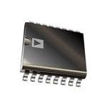
| 供应商器件封装 | 16-TSSOP |
| 信噪比 | 60 dB |
| 分辨率 | 10 bit |
| 分辨率(位) | 10 b |
| 功能 | Waveform generator |
| 包装 | 管件 |
| 商标 | Analog Devices |
| 字宽调谐(位) | 24 b |
| 安装类型 | 表面贴装 |
| 安装风格 | SMD/SMT |
| 封装 | Tube |
| 封装/外壳 | 16-TSSOP(0.173",4.40mm 宽) |
| 封装/箱体 | TSSOP-16 |
| 工作温度 | -40°C ~ 125°C |
| 工作温度范围 | - 40 C to + 105 C |
| 工作电源电压 | 2.3 V to 5.5 V |
| 工厂包装数量 | 96 |
| 标准包装 | 96 |
| 电压-电源 | 2.3 V ~ 5.5 V |
| 系列 | AD5932 |
| 视频文件 | http://www.digikey.cn/classic/video.aspx?PlayerID=1364138032001&width=640&height=505&videoID=2245193148001 |
| 转换器数量 | 1 |


- 商务部:美国ITC正式对集成电路等产品启动337调查
- 曝三星4nm工艺存在良率问题 高通将骁龙8 Gen1或转产台积电
- 太阳诱电将投资9.5亿元在常州建新厂生产MLCC 预计2023年完工
- 英特尔发布欧洲新工厂建设计划 深化IDM 2.0 战略
- 台积电先进制程称霸业界 有大客户加持明年业绩稳了
- 达到5530亿美元!SIA预计今年全球半导体销售额将创下新高
- 英特尔拟将自动驾驶子公司Mobileye上市 估值或超500亿美元
- 三星加码芯片和SET,合并消费电子和移动部门,撤换高东真等 CEO
- 三星电子宣布重大人事变动 还合并消费电子和移动部门
- 海关总署:前11个月进口集成电路产品价值2.52万亿元 增长14.8%
PDF Datasheet 数据手册内容提取
Programmable Frequency Scan Waveform Generator Data Sheet AD5932 FEATURES GENERAL DESCRIPTION Programmable frequency profile The AD59321 is a waveform generator offering a programmable No external components necessary frequency scan. Utilizing embedded digital processing that Output frequency up to 25 MHz allows enhanced frequency control, the device generates Preprogrammable frequency profile minimizes number of synthesized analog or digital frequency-stepped waveforms. DSP/microcontroller writes Because frequency profiles are preprogrammed, continuous Sinusoidal/triangular/square wave outputs write cycles are eliminated, thereby freeing up valuable Automatic or single pin control of frequency stepping DSP/microcontroller resources. Waveforms start from a known Power-down mode: 20 µA phase and are incremented phase-continuously, which allows Power supply: 2.3 V to 5.5 V phase shifts to be easily determined. Consuming only 6.7 mA, Automotive temperature range: −40°C to +125°C the AD5932 provides a convenient low power solution to 16-lead, Pb-free TSSOP waveform generation. APPLICATIONS The AD5932 outputs each frequency in the range of interest for a defined length of time and then steps to the next frequency in Frequency scanning/radar the scan range. The length of time the device outputs a particular Network/impedance measurements frequency is preprogrammed, and the device increments the Incremental frequency stimulus Sensory applications frequency automatically; or, alternatively, the frequency is Proximity and motion incremented externally via the CTRL pin. At the end of the range, the AD5932 continues to output the last frequency until the device is reset. The AD5932 also offers a digital output via the MSBOUT pin. (continued on Page 3) FUNCTIONAL BLOCK DIAGRAM DVDD CAP/2.5V DGND INTERRUPT STANDBY AGND AVDD REGULATOR AD5932 VCC BUFFER SYNCOUT 2.5V MCLK SYNC BUFFER MSBOUT INCREMENT CTRL CONTROLLER 24-BIT DATA INCR PIPELINED DDS CORE 10-BIT VOUT DAC FREQUENCY / CONTROLLER 24 DATAAND CONTROL SERIAL INTERFACE CONTROL ON-BOARD FULL-SCALE REGISTER REFERENCE CONTROL COMP FSYNC SCLK SDATA 05416-001 Figure 1. 1 Protected by U.S. patent number 6747583. Rev. C Document Feedback Information furnished by Analog Devices is believed to be accurate and reliable. However, no responsibility is assumed by Analog Devices for its use, nor for any infringements of patents or other One Technology Way, P.O. Box 9106, Norwood, MA 02062-9106, U.S.A. rights of third parties that may result from its use. Specifications subject to change without notice. No license is granted by implication or otherwise under any patent or patent rights of Analog Devices. Tel: 781.329.4700 ©2006–2017 Analog Devices, Inc. All rights reserved. Trademarks and registered trademarks are the property of their respective owners. Technical Support www.analog.com
AD5932 Data Sheet TABLE OF CONTENTS Features .............................................................................................. 1 Serial Interface ............................................................................ 15 Applications ....................................................................................... 1 Powering up the AD5932 .......................................................... 15 General Description ......................................................................... 1 Programming the AD5932 ........................................................ 16 Functional Block Diagram .............................................................. 1 Setting Up the Frequency Scan................................................. 17 Revision History ............................................................................... 2 Activating and Controlling the Scan ....................................... 18 Specifications ..................................................................................... 4 Outputs from the AD5932 ........................................................ 19 Specifications Test Circuit ........................................................... 5 Applications ..................................................................................... 20 Timing Specifications .................................................................. 6 Grounding and Layout .............................................................. 20 Master Clock and Timing Diagrams ......................................... 6 AD5932 to the ADSP-BF527 Interface .................................... 20 Absolute Maximum Ratings ............................................................ 8 AD5932 to 68HC11/68L11 Interface ....................................... 20 ESD Caution .................................................................................. 8 AD5932 to 80C51/80L51 Interface .......................................... 21 Pin Configuration and Function Descriptions ............................. 9 AD5932 to DSP56002 Interface ............................................... 21 Typical Performance Characteristics ........................................... 10 Evaluation Board ............................................................................ 22 Terminology .................................................................................... 14 Schematics ................................................................................... 23 Theory of Operation ...................................................................... 15 Outline Dimensions ....................................................................... 25 Frequency Profile........................................................................ 15 Ordering Guide .......................................................................... 25 REVISION HISTORY 4/2017—Rev. B to Rev. C 2/2012—Rev. 0 to Rev. A Changes to AD5932 to 68HC11/68L11 Interface Section ........ 20 Changes to Figure 21, Figure 22, Figure 23, Figure 24, and Figure 25 .......................................................................................... 12 11/2016—Rev. A to Rev. B Changes to Figure 26, Figure 27, Figure 28, and Figure 29 ....... 13 Changed ADSP-21xx to ADSP-BF527 ........................ Throughout Changes to Features Section............................................................ 1 4/2006—Revision 0: Initial Version Changes to AD5932 to the ADSP-BF527 Interface Section and Figure 34 .......................................................................................... 20 Rev. C | Page 2 of 28
Data Sheet AD5932 GENERAL DESCRIPTION (continued from Page 1) To program the AD5932, the user enters the start frequency, the Note that the AVDD and DVDD are independent of each other increment step size, the number of increments to be made, and and can be operated from different voltages. The AD5932 also the time interval that the part outputs each frequency. The fre- has a standby function that allows sections of the device that are quency scan profile is initiated, started, and executed by toggling not in use to be powered down. the CTRL pin. The AD5932 is available in a 16-lead, Pb-free TSSOP. The AD5932 is written to via a 3-wire serial interface that operates at clock rates up to 40 MHz. The device operates with a power supply from 2.3 V to 5.5 V. Rev. C | Page 3 of 28
AD5932 Data Sheet SPECIFICATIONS AVDD = DVDD = 2.3 V to 5.5 V; AGND = DGND = 0 V; T = T to T , unless otherwise noted. A MIN MAX Table 1. Y Grade1 Parameter Min Typ Max Unit Test Conditions/Comments SIGNAL DAC SPECIFICATIONS Resolution 10 Bits Update Rate 50 MSPS VOUT Peak-to-Peak 0.58 V Internal 200 Ω resistor to GND VOUT Offset 56 mV From 0 V to the trough of the waveform V 0.32 V Voltage at midscale output MIDSCALE VOUT TC 200 ppm/°C DC Accuracy Integral Nonlinearity (INL) ±1.5 LSB Differential Nonlinearity (DNL) ±0.75 LSB DDS SPECIFICATIONS Dynamic Specifications Signal-to-Noise Ratio 53 60 dB f = 50 MHz, f = f /4096 MCLK OUT MCLK Total Harmonic Distortion −60 −53 dBc f = 50 MHz, f = f /4096 MCLK OUT MCLK Spurious-Free Dynamic Range (SFDR) Wide Band (0 to Nyquist) −56 −52 dBc f = 50 MHz, f = f /50 MCLK OUT MCLK Narrow Band (±200 kHz) −74 −70 dBc f = 50 MHz, f = f /50 MCLK OUT MCLK Clock Feedthrough −50 dBc Up to 16 MHz out Wake-Up Time 1.7 ms From standby OUTPUT BUFFER VOUT Peak-to-Peak 0 DVDD V Typically, square wave on MSBOUT and SYNCOUT Output Rise/Fall Time2 12 ns VOLTAGE REFERENCE Internal Reference 1.15 1.18 1.26 V Reference TC2 90 ppm/°C LOGIC INPUTS2 Input Current 0.1 ±2 µA Input High Voltage, V 1.7 V DVDD = 2.3 V to 2.7 V INH 2.0 V DVDD = 2.7 V to 3.6 V 2.8 V DVDD = 4.5 V to 5.5 V Input Low Voltage, V 0.6 V DVDD = 2.3 V to 2.7 V INL 0.7 V DVDD = 2.7 V to 3.6 V 0.8 V DVDD = 4.5 V to 5.5 V Input Capacitance, C 3 pF IN LOGIC OUTPUTS2 Output High Voltage, V DVDD − 0.4 V V I = 1 mA OH SINK Output Low Voltage, V 0.4 V I = 1 mA OL SINK Floating-State O/P Capacitance 5 pF POWER REQUIREMENTS f = 50 MHz, f = f /7 MCLK OUT MCLK AVDD/DVDD 2.3 5.5 V I 3.8 4 mA AA I 2.4 2.7 mA DD I + I 6.2 6.7 mA AA DD Rev. C | Page 4 of 28
Data Sheet AD5932 Y Grade1 Parameter Min Typ Max Unit Test Conditions/Comments Low Power Sleep Mode Device is reset before putting into standby 20 85 µA All outputs powered down, MCLK = 0 V, serial interface active 140 240 µA All outputs powered down, MCLK active, serial interface active 1 Operating temperature range is as follows: Y version: −40°C to +125°C; typical specifications are at +25°C. 2 Guaranteed by design, not production tested. SPECIFICATIONS TEST CIRCUIT 100nF 10nF AVDD 10nF CAP/2.5V COMP REGULATOR 12 SIN 10-BIT VOUT ROM DAC AD5932 20pF 05416-002 Figure 2. Test Circuit Used to Test the Specifications Rev. C | Page 5 of 28
AD5932 Data Sheet TIMING SPECIFICATIONS All input signals are specified with t = t = 5 ns (10% to 90% of V ) and are timed from a voltage level of (V + V )/2 (see Figure 3 to R F DD IL IH Figure 6). DVDD = 2.3 V to 5.5 V; AGND = DGND = 0 V; all specifications T to T , unless otherwise noted. MIN MAX Table 2. Parameter1 Limit at T , T Unit Conditions/Comments MIN MAX t 20 ns min MCLK period 1 t 8 ns min MCLK high duration 2 t 8 ns min MCLK low duration 3 t 25 ns min SCLK period 4 t 10 ns min SCLK high time 5 t 10 ns min SCLK low time 6 t 5 ns min FSYNC to SCLK falling edge setup time 7 t 10 ns min FSYNC to SCLK hold time 8 t 5 ns min Data setup time 9 t 3 ns min Data hold time 10 t 2 × t ns min Minimum CTRL pulse width 11 1 t 0 ns min CTRL rising edge to MCLK falling edge setup time 12 t 10 × t ns typ CTRL rising edge to VOUT delay (initial pulse, includes initialization) 13 1 8 × t ns typ CTRL rising edge to VOUT delay (initial pulse, includes initialization) 1 t 1 × t ns typ Frequency change to SYNC output, each frequency increment 14 1 t 2 × t ns typ Frequency change to SYNC output, end of scan 15 1 t 20 ns max MCLK falling edge to MSBOUT 16 1 Guaranteed by design, not production tested. MASTER CLOCK AND TIMING DIAGRAMS t1 MCLK t2 t3 05416-003 Figure 3. Master Clock t5 t4 SCLK t7 t6 t8 FSYNC t10 SDATA D15 D14 D2 t9 D1 D0 D15 D14 05416-004 Figure 4. Serial Timing t12 MCLK CTRL t11 VOUT t13 05416-005 Figure 5. CTRL Timing Rev. C | Page 6 of 28
Data Sheet AD5932 CTRL t13 VOUT SYNCOUT (Each Frequency Increment) t14 (EnSdY oNf CSOcaUnT) t15 05416-006 Figure 6. SYNCOUT Timing Rev. C | Page 7 of 28
AD5932 Data Sheet ABSOLUTE MAXIMUM RATINGS ESD CAUTION T = 25°C, unless otherwise noted. A Table 3. Parameter Rating AVDD to AGND −0.3 V to +6.0 V DVDD to DGND −0.3 V to +6.0 V AGND to DGND −0.3 V to +0.3 V CAP/2.5 V to DGND −0.3 V to +2.75 V Digital I/O Voltage to DGND −0.3 V to DVDD + 0.3 V Analog I/O Voltage to AGND −0.3 V to AVDD + 0.3 V Operating Temperature Range Automotive (Y Version) −40°C to +125°C Storage Temperature Range −65°C to +150°C Maximum Junction Temperature +150°C TSSOP (4-Layer Board) θ Thermal Impedance 112°C/W JA θ Thermal Impedance 27.6°C/W JC Reflow Soldering (Pb-Free) 300°C Peak Temperature 260(+0/−5)°C Time at Peak Temperature 10 sec to 40 sec Stresses at or above those listed under Absolute Maximum Ratings may cause permanent damage to the product. This is a stress rating only; functional operation of the product at these or any other conditions above those indicated in the operational section of this specification is not implied. Operation beyond the maximum operating conditions for extended periods may affect product reliability. Rev. C | Page 8 of 28
Data Sheet AD5932 PIN CONFIGURATION AND FUNCTION DESCRIPTIONS COMP 1 16 VOUT AVDD 2 15 AGND DVDD 3 14 STANDBY AD5932 CAP/2.5V 4 TOP VIEW 13 FSYNC DGND 5 (Not to Scale) 12 SCLK MCLK 6 11 SDATA SYNCOUT 7 10 CTRL MSBOUT 8 9 INTERRUPT05416-007 Figure 7. Pin Configuration Table 4. Pin Function Descriptions Pin No. Mnemonic Description 1 COMP DAC Bias Pin. This pin is used for decoupling the DAC bias voltage to AVDD. 2 AVDD Positive Power Supply for the Analog Section. AVDD can have a value from 2.3 V to 5.5 V. A 0.1 µF decoupling capacitor should be connected between AVDD and AGND. 3 DVDD Positive Power Supply for the Digital Section. DVDD can have a value from 2.3 V to 5.5 V. A 0.1 µF decoupling capacitor should be connected between DVDD and DGND. 4 CAP/2.5V Digital Circuitry. Operates from a 2.5 V power supply. This 2.5 V is generated from DVDD using an on-board regulator. The regulator requires a decoupling capacitor of typically 100 nF, which is connected from CAP/2.5V to DGND. If DVDD is equal to or less than 2.7 V, CAP/2.5V can be shorted to DVDD. 5 DGND Ground for All Digital Circuitry. 6 MCLK Digital Clock Input. DDS output frequencies are expressed as a binary fraction of the frequency of MCLK. The output frequency accuracy and phase noise are determined by this clock. 7 SYNCOUT Digital Output for Scan Status Information. User-selectable for end of scan (EOS) or frequency increments through the control register (SYNCOP bit). This pin must be enabled by setting the SYNCOUTEN bit in the control register to 1. 8 MSBOUT Digital Output. The inverted MSB of the DAC data is available at this pin. This output pin must be enabled by setting the MSBOUTEN bit in the control register to 1. 9 INTERRUPT Digital Input. This pin acts as an interrupt during a frequency scan. A low-to-high transition is sampled by the internal MCLK, which resets internal state machines. This results in the DAC output going to midscale. 10 CTRL Digital Input. Triple function pin for initialization, start, and external frequency increments. A low-to-high transition, sampled by the internal MCLK, is used to initialize and start internal state machines, which then execute the pre-programmed frequency scan sequence. When in auto-increment mode, a single pulse executes the entire scan sequence. When in external increment mode, each frequency increment is triggered by low-to-high transitions. 11 SDATA Serial Data Input. The 16-bit serial data-word is applied to this input with the register address first, followed by the MSB to LSBs of the data. 12 SCLK Serial Clock Input. Data is clocked into the AD5932 on each falling SCLK edge. 13 FSYNC Active Low Control Input. This is the frame synchronization signal for the serial data. When FSYNC is taken low, the internal logic is informed that a new word is being loaded into the device. 14 STANDBY Active High Digital Input. When this pin is high, the internal MCLK is disabled, and the reference DAC and regulator are powered down. For optimum power saving, it is recommended that the AD5932 be reset before it is put into standby, as this results in a shutdown current of typically 20 µA. 15 AGND Ground for All Analog Circuitry. 16 VOUT Voltage Output. The analog outputs from the AD5932 are available here. An external resistive load is not required, because the device has a 200 Ω resistor on board. A 20 pF capacitor to AGND is recommended to act as a low-pass filter and to reduce clock feedthrough. Rev. C | Page 9 of 28
AD5932 Data Sheet TYPICAL PERFORMANCE CHARACTERISTICS 9 –40 TA = 25°C AVDD = DVDD = 3V/5V 8 AVDD = 5V –45 MCLK = 50MHz MSBOUT, SYNCOUT ENABLED CREG = 011111111111 7 DVDD = 5V –50 TA = 25°C FOUT = MCLK/7 –55 6 I (mA)DD 45 DVDD = 3V SFDR (dBc) –––667050 FOUT = MCLK/50 3 DVDD = 5V, FOUT = MCLK/7 –75 FOUT = MCLK/3 2 –80 10 DVDD = 3V, FOUT = MCLK/7 05416-008 ––8950 05416-011 0 5 10 15 20 25 30 35 40 45 50 0 5 10 15 20 25 30 35 40 45 50 MCLK FREQUENCY (MHz) MCLK FREQUENCY (MHz) Figure 8. Current Consumption (IDD) vs. MCLK Frequency Figure 11. Wide-Band SFDR vs. MCLK Frequency 7 –60 MTAC =L K2 5=° C50MHz MSBOUT ON, AMVCDLDK == D50VMDHDz = 3V/5V 6 SYNCOUT ON –65 CREG = 011111111111 TA = 25°C 5 MSBOUT OFF, –70 FOUT = MCLK/50 I (mA)DD 43 SYNCOUT ON SMYSNBCOOUUTT OONF,F SFDR (dBc) –75 FOUT = MCLK/3 MSBOUT OFF, –80 2 SYNCOUT OFF 10 05416-009 ––8950 FOUT = MCLK/7 05416-012 1kHz 100kHz 1MHz 5MHz 15MHz 25MHz 0 5 10 15 20 25 30 35 40 45 50 500kHz 10kHz 500kHz 2MHz 10MHz 20MHz MCLK FREQUENCY (MHz) FOUT (Hz) Figure 9. IDD vs. FOUT for Various Digital Output Conditions Figure 12. Narrow-Band SFDR vs. MCLK Frequency 3.5 –30 AVDD = DVDD = 3V/5V 3.0 AIDD –40 CTAR E=G 2 =5 °0C11111111111 MCLK = 50MHz 2.5 –50 DIDD c) A) 2.0 dB (mD DR ( –60 ID 1.5 SF MCLK = 10MHz –70 1.0 MCLK = 1MHz LEGEND MCLK = 30MHz 1. SINEWAVE OUTPUT, INTERNALLY CONTROLLED SWEEP –80 0.50 234... TSTRRINIIAAENNWGGAUUVLLEAA ORR UOOTUUPTTUPPTUU, ETT,,X IETNXETTREENRRANNLAALLLYLL YCY OC CONOTNNRTTORROLOLLLELLDEE DSD WS SWEWEEEPEEPP 05416-010 –90 05416-013 1 2 3 4 0.001 0.01 0.1 1 10 100 CONTROL OPTION (See Legend) FOUT (MHz) Figure 10. IDD vs. Output Waveform Type and Control Figure 13. Wideband SFDR vs. FOUT for Various MCLK Frequencies Rev. C | Page 10 of 28
Data Sheet AD5932 70 90 TA = 25°C AVDD = DVDD = 5V 80 65 fOUT = FMCLK/4096 70 S 60 CE 60 VI R (dB) 55 OF DE 50 SN ER 40 B M 50 U 30 N 20 45 40 05416-014 100 05416-017 0 10M 20M 30M 40M 50M 656667686970717273747576777879808182838485868788899091929394959697 555555555555555555555555555555555 MCLK FREQUENCY (MHz) Vp-p (mV) Figure 14. SNR vs. MCLK Frequency Figure 17. Histogram of VOUT Peak-to-Peak 80 1.25 AVDD = DVDD = 5V 70 1.23 60 S E C VI 50 E 1.21 D (V)EF R OF 40 R E V 1.19 MB 30 U N 20 1.17 1.15 05416-015 100 505152535455565758596061626364656667686970 05416-018 –40 –20 0 20 40 60 80 100 120 TEMPERATURE (°C) VOFFSET (mV) Figure 15. VREF vs. Temperature Figure 18. Histogram of VOUT Offset 0 2.0 TA = 25°C –10 100mV p-p RIPPLE 1.9 AVDD = DVDD = 2.3V NO DECOUPLING ON SUPPLIES AVDD = DVDD = 5V –20 1.8 E (ms) 1.7 AVDD = DVDD = 5V ON (dB) –30 DVDD (on CAP/2.5V) E-UP TIM 1.6 TENUATI ––4500 AK 1.5 AT W –60 1.4 11..32 05416-016 ––780010 100 1k AVDD (1o0nk VOUT)100k 1M05416-019 –40 –20 0 20 40 60 80 100 120 TEMPERATURE (°C) MODULATING FREQUENCY (Hz) Figure 16. Wake-up Time vs. Temperature Figure 19. PSSR Rev. C | Page 11 of 28
AD5932 Data Sheet 0 0 –10 –20 –10 –30 –20 –40 –50 –30 E –60 OIS –70 –40 SE N ––8900 (dB) –50 A H –100 –60 P –110 –120 –70 –130 –80 –140 –––111567000 05416-020 –1–0900 05416-023 100 1k 10k 100k 0 5M FREQUENCY (Hz) RWB 1K VWB 300 ST 50 SEC FREQUENCY (Hz) Figure 20. Output Phase Noise Figure 23. fMCLK = 10 MHz, fOUT = 3.33 MHz = fMCLK/3, Frequency Word = 555555 0 0 –10 –10 –20 –20 –30 –30 –40 –40 (dB) –50 (dB) –50 –60 –60 –70 –70 –80 –80 –1–0900 05416-021 –1–0900 05333-017 0 100k 0 160k RWB 100 VWB 30 ST 100 SEC RWB 100 VWB 30 ST 200 SEC FREQUENCY (Hz) FREQUENCY (Hz) Figure 21. fMCLK = 10 MHz, fOUT = 2.4 kHz, Figure 24. fMCLK = 50 MHz, fOUT = 12 kHz, Frequency Word = 000FBA Frequency Word = 000FBA 0 0 –10 –10 –20 –20 –30 –30 –40 –40 (dB) –50 (dB) –50 –60 –60 –70 –70 –80 –80 –1–0900 05416-022 –1–0900 05416-025 0 5M 0 1.6M RWB 1K VWB 300 ST 50 SEC RWB 100 VWB 300 ST 200 SEC FREQUENCY (Hz) FREQUENCY (Hz) Figure 22. fMCLK = 10 MHz, fOUT = 1.43 MHz = fMCLK/7, Figure 25. fMCLK = 50 MHz, fOUT = 120 kHz, Frequency Word = 249249 Frequency Word = 009D49 Rev. C | Page 12 of 28
Data Sheet AD5932 0 0 –10 –10 –20 –20 –30 –30 –40 –40 dB) –50 dB) –50 ( ( –60 –60 –70 –70 –80 –80 –1–0900 05416-026 –1–0900 05416-028 0 25M 0 25M RWB 1K VWB 300 ST 200 SEC RWB 1K VWB 300 ST 200 SEC FREQUENCY (Hz) FREQUENCY (Hz) Figure 26. fMCLK = 50 MHz, fOUT = 1.2 MHz, Figure 28. fMCLK = 50 MHz, fOUT = 7.143 MHz = fMCLK/7, Frequency Word = 0624DD Frequency Word = 249249 0 0 –10 –10 –20 –20 –30 –30 –40 –40 (dB) –50 dB) –50 ( –60 –60 –70 –70 –80 –80 –1–09000 25M05416-027 –1–0900 05416-029 0 25M RWB 1K VWB 300 ST 200 SEC RWB 1K VWB 300 ST 200 SEC FREQUENCY (Hz) FREQUENCY (Hz) Figure 27. fMCLK = 50 MHz, fOUT = 4.8 MHz, Figure 29. fMCLK = 50 MHz, fOUT = 16.667 MHz = fMCLK/3, Frequency Word = 189374 Frequency Word = 555555 Rev. C | Page 13 of 28
AD5932 Data Sheet TERMINOLOGY Integral Nonlinearity (INL) Total Harmonic Distortion (THD) Integral nonlinearity is the maximum deviation of any code Total harmonic distortion is the ratio of the rms sum of from a straight line passing through the endpoints of the harmonics to the rms value of the fundamental. For the transfer function. The endpoints of the transfer function are AD5932, THD is defined as: zero scale and full scale. The error is expressed in LSBs. V 2 +V 2 +V 2 +V 2 +V 2 Differential Nonlinearity (DNL) THD(dB)=20log 2 3 4 5 6 V Differential nonlinearity is the difference between the measured 1 and ideal 1 LSB change between two adjacent codes in the DAC. where: A specified differential nonlinearity of ±1 LSB maximum V is the rms amplitude of the fundamental. 1 ensures monotonicity. V, V, V, V, and V are the rms amplitudes of the second 2 3 4 5 6 Spurious-Free Dynamic Range (SFDR) through the sixth harmonic. Along with the frequency of interest, harmonics of the Signal-to-Noise Ratio (SNR) fundamental frequency and images of these frequencies are The signal-to-noise ratio is the ratio of the rms value of the present at the output of a DDS device. The SFDR refers to the measured output signal to the rms sum of all other spectral largest spur or harmonic that is present in the band of interest. components below the Nyquist frequency. The value for SNR is The wideband SFDR gives the magnitude of the largest harmonic expressed in dB. or spur relative to the magnitude of the fundamental frequency Clock Feedthrough in the 0 to Nyquist bandwidth. The narrow-band SFDR gives There is feedthrough from the MCLK input to the analog the attenuation of the largest spur or harmonic in a bandwidth output. Clock feedthrough refers to the magnitude of the of ±200 kHz about the fundamental frequency. MCLK signal relative to the fundamental frequency in the AD5932 output spectrum. Rev. C | Page 14 of 28
Data Sheet AD5932 THEORY OF OPERATION The AD5932 is a general-purpose, synthesized waveform generator capable of providing digitally programmable waveform sequences in both the frequency and time domain. FINAL FREQUENCY The device contains embedded digital processing to provide a OUT scan of a user-programmable frequency profile allowing enhanced frequency control. Because the device is preprogrammable, it eliminates continuous write cycles from a DSP/microcontroller in generating a particular waveform. FSTART FREQUENCY PROFILE MIDSCALE 05416-031 The frequency profile is defined by the start frequency (FSTART), Figure 31. Frequency Scan the frequency increment (Δf) and the number of increments SERIAL INTERFACE per scan (N ). The increment interval between frequency INCR increments, t , is either user-programmable with the interval The AD5932 has a standard 3-wire serial interface that is INT automatically determined by the device (auto-increment mode), compatible with SPI®, QSPI™, MICROWIRE™, and DSP or externally controlled via a hardware pin (external increment interface standards. mode). For automatic update, the interval profile can be for Data is loaded into the device as a 16-bit word under the either a fixed number of clock periods or a fixed number of control of a serial clock input, SCLK. The timing diagram for output waveform cycles. this operation is shown in Figure 4. In the auto-increment mode, a single pulse at the CTRL pin starts The FSYNC input is a level-triggered input that acts as a frame and executes the frequency scan. In the external-increment mode, synchronization and chip enable. Data can be transferred into the the CTRL pin also starts the scan, but the frequency increment device only when FSYNC is low. To start the serial data transfer, interval is determined by the time interval between sequential FSYNC should be taken low, observing the minimum FSYNC to 0/1 transitions on the CTRL pin. SCLK falling edge setup time, t. After FSYNC goes low, serial 7 An example of a 2-step frequency scan is shown in Figure 30. data is shifted into the device's input shift register on the falling Note the frequency swept output signal is continuously available edges of SCLK for 16 clock pulses. FSYNC may be taken high and is, therefore, phase continuous at all frequency increments. after the 16th falling edge of SCLK, observing the minimum SCLK falling edge to FSYNC rising edge time, t Alternatively, 8. FSYNC can be kept low for a multiple of 16 SCLK pulses and then brought high at the end of the data transfer. In this way, a continuous stream of 16-bit words can be loaded while FSYNC is held low. FSYNC should only go high after the 16th SCLK falling edge of the last word is loaded. N1UMBER OF STEP CHANGE2S 05416-030 The SCLK can be continuous, or, alternatively, the SCLK can Figure 30. Operation of the AD5932 idle high or low between write operations. When the AD5932 completes the frequency scan from POWERING UP THE AD5932 frequency start to frequency end, that is, from FSTART When the AD5932 is powered up, the part is in an undefined incrementally to (FSTART + NINCR × Δf), it continues to output state and, therefore, must be reset before use. The seven registers the last frequency in the scan (see Figure 31). Note that the (control and frequency) contain invalid data and need to be set frequency scan time is given by (NINCR + 1) × tINT. to a known value by the user. The control register should be the first register to be programmed, as this sets up the part. Note that a write to the control register automatically resets the internal state machines and provides an analog output of midscale, because it performs the same function as the INTERRUPT pin. Typically, this is followed by a serial loading of all the required scan parameters. The DAC output remains at midscale until a frequency scan is started using the CTRL pin. Rev. C | Page 15 of 28
AD5932 Data Sheet PROGRAMMING THE AD5932 Table 5. Register Addresses Register Address The AD5932 is designed to provide automatic frequency scans D15 D14 D13 D12 Mnemonic Name when the CTRL pin is triggered. The scan is controlled by a set 0 0 0 0 C Control bits REG of registers, the addresses of which are given in Table 5. The 0 0 0 1 N Number of increments INCR function of each register is described in more detail in the 0 0 1 0 ∆f Lower 12 bits of Setting Up the Frequency Scan section. delta frequency The Control Register 0 0 1 1 ∆f Higher 12 bits of delta frequency The AD5932 contains a 12-bit control register that sets up the 0 1 t Increment interval operating modes, as shown in the following bit map. INT 1 0 Reserved D15 D14 D13 D12 D11 to D0 1 1 0 0 F Lower 12 bits of START 0 0 0 0 Control bits start frequency 1 1 0 1 F Higher 12 bits of This register controls the different functions and the various START start frequency output options from the AD5932. Table 6 describes the 1 1 1 0 Reserved individual bits of the control register. 1 1 1 1 Reserved To address the control register, D15 to D12 of the 16-bit serial word must be set to 0. Table 6. Description of Bits in the Control Register Bit Name Function D15 to D12 ADDR Register address bits. D11 B24 Two write operations are required to load a complete word into the F register and the Δf register. START When B24 = 1, a complete word is loaded into a frequency register in two consecutive writes. The first write contains the 12 LSBs of the frequency word and the next write contains the 12 MSBs. Refer to Table 5 for the appropriate addresses. The write to the destination register occurs after both words have been loaded, so the register never holds an intermediate value. When B24 = 0, the 24-bit F /Δf register operates as two 12-bit registers, one containing the 12 MSBs START and the other containing the 12 LSBs. This means that the 12 MSBs of the frequency word can be altered independently of the 12 LSBs and vice versa. This is useful if the complete 24-bit update is not required. To alter the 12 MSBs or the 12 LSBs, a single write is made to the appropriate register address. Refer to Table 5 for the appropriate addresses. D10 DAC ENABLE When DAC ENABLE = 1, the DAC is enabled. When DAC ENABLE = 0, the DAC is powered down. This saves power and is beneficial when using only the MSB of the DAC input data (available at the MSBOUT pin). D9 SINE/TRI The function of this bit is to control what is available at the VOUT pin. When SINE/TRI = 1, the SIN ROM is used to convert the phase information into amplitude information, resulting in a sinusoidal signal at the output. When SINE/TRI = 0, the SIN ROM is bypassed, resulting in a triangular (up-down) output from the DAC. D8 MSBOUTEN When MSBOUTEN = 1, the MSBOUT pin is enabled. When MSBOUTEN = 0, the MSBOUT is disabled (three-state). D7 Reserved This bit must be set to 1. D6 Reserved This bit must be set to 1. D5 INT/EXT INCR When INT/EXT INCR = 1, the frequency increments are triggered externally through the CTRL pin. When INT/EXT INCR = 0, the frequency increments are triggered automatically. D4 Reserved This bit must be set to 1. D3 SYNCSEL This bit is active when D2 = 1. It is user-selectable to pulse at end of scan (EOS) or at each frequency increment. When SYNCSEL = 1, the SYNCOUT pin outputs a high level at end of scan and returns to 0 at the start of the subsequent scan. When SYNCSEL= 0, the SYNCOUT outputs a pulse of 4 × T only at each frequency increment. CLOCK D2 SYNCOUTEN When SYNCOUTEN = 1, the SYNC output is available at the SYNCOUT pin. When SYNCOUTEN = 0, the SYNCOP pin is disabled (three-state). D1 Reserved This bit must be set to 1. D0 Reserved This bit must be set to 1. Rev. C | Page 16 of 28
Data Sheet AD5932 SETTING UP THE FREQUENCY SCAN Number of Increments (N ) INCR As stated in the Frequency Profile section, the AD5932 requires An end frequency is not required on the AD5932. Instead, this certain registers to be programmed to enable a frequency scan. end frequency is calculated by multiplying the frequency increment The Setting Up the Frequency Scan section discusses these value (Δf) by the number of frequency steps (NINCR) and adding registers in more detail. it to/subtracting it from the start frequency (FSTART); that is, F + N × Δf. The N register is a 12-bit register, with Start Frequency (F ) START INCR INCR START the address shown in the following bit map. To start a frequency scan, the user needs to tell the AD5932 D15 D14 D13 D12 D11 D0 what frequency to start scanning from. This frequency is stored 0 0 0 1 12 bits of N <11…0> in a 24-bit register called F . If the user wishes to alter the INCR START entire contents of the FSTART register, two consecutive writes The number of increments is programmed in binary fashion, must be performed: one to the LSBs and the other to the MSBs. with 000000000010 representing the minimum number of Note that for an entire write to this register, Control Bit B24 frequency increments (two increments) and 111111111111 (D11) should be set to 1, with the LSBs programmed first. representing the maximum number of increments (4095). In some applications, the user does not need to alter all 24 bits Table 8. N Data Bits INCR of the F register. By setting Control Bit B24 (D11) to 0, the START D11 … D0 Number of Increments 24-bit register operates as two 12-bit registers, one containing 0000 0000 0010 Two frequency increments. This is the the 12 MSBs and the other containing the 12 LSBs. This means minimum number of frequency that the 12 MSBs of the FSTART word can be altered independently increments. of the 12 LSBs and vice versa. The addresses of both the LSBs 0000 0000 0011 Three frequency increments. and the MSBs of this register are shown in the following bit map. 0000 0000 0100 Four frequency increments. D15 D14 D13 D12 D11 to D0 … … … … 1 1 0 0 12 LSBs of F <11…0> 1111 1111 1110 4094 frequency increments. START 1 1 0 1 12 MSBs of F <23…12> 1111 1111 1111 4095 frequency increments. START Frequency Increments (∆f) Increment Interval (tINT) The value in the Δf register sets the increment frequency for the The increment interval dictates the duration of the DAC output scan and is added incrementally to the current output frequency. signal for each individual frequency of the frequency scan. The Note that the increment frequency can be positive or negative, AD5932 offers the user two choices: thereby giving an increasing or decreasing frequency scan. • The duration is a multiple of cycles of the output frequency. At the start of a scan, the frequency contained in the FSTART • The duration is a multiple of MCLK periods. register is output. Next, the frequency (F + Δf ) is output. START The desired choice is selected by Bit D13 in the t register as This is followed by (F + Δf + Δf), and so on. Multiplying INT START shown in the following bit map. the Δf value by the number of increments (N ) and adding it INCR to the start frequency (F ) give the final frequency in the D15 D14 D13 D12 D11 D10 to D0 START scan. Mathematically, this final frequency/stop frequency is 0 1 0 x x 11 bits <10…0> represented by Fixed number of output waveform cycles. F + (N × Δf) START INCR 0 1 1 x x 11 bits <10…0> The Δf register is a 23-bit register that requires two 16-bit writes Fixed number of clock periods. to be programmed. Table 7 gives the addresses associated with both the MSB and LSB registers of the Δf word. Programming of this register is in binary form, with the minimum number being decimal 2. Note that 11 bits, D10 to Table 7. Δf Register Bits D0, of the register are available to program the time interval. As Scan an example, if MCLK = 50 MHz, then each clock period/base D15 D14 D13 D12 D11 D10 to D0 Direction interval is (1/50 MHz) = 20 ns. If each frequency must be output 0 0 1 0 12 LSBs of ∆f N/A for 100 ns, then <00000000101> or decimal 5 must be pro- <11…0> grammed to this register. Note that the AD5930 can output each 0 0 1 1 0 11 MSBs of Δf Positive Δf <22…12> (F + Δf) frequency for a maximum duration of 211 − 1 (or 2047) times START 0 0 1 1 1 11 MSBs of Δf Negative ∆f the increment interval. <22…12> (F − Δf) START Rev. C | Page 17 of 28
AD5932 Data Sheet Therefore, in this example, a time interval of 20 ns × 2047 = 40 µs Auto-Increment Control is the maximum, with the minimum being 40 ns. For some The value in the t register is used to control the scan. The INT applications, this maximum time of 40 µs may be insufficient. AD5932 outputs each frequency for the length of time pro- Therefore, to allow for sweeps that need a longer increment grammed in the T register, before moving on to the next INT interval, time-base multipliers are provided. D12 and D11 are frequency. dedicated to the time-base multipliers, as shown in the bit map To set up the AD5932 to this mode, INT/EXT INCR (Bit D5) above. A more detailed table of the multiplier options is given in must be set to 0. Table 9. External Increment Control Table 9. Time-Base Multiplier Values In this case, the time interval, t , is set by the pulse rate on the D12 D11 Multiplier Value INT CTRL pin. The first 0 to 1 transition on the pin starts the scan. 0 0 Multiply (1/MCLK) by 1 Each subsequent 0 to 1 transition on the CTRL pin increments 0 1 Multiply (1/MCLK) by 5 the output frequency by the value programmed into the ∆f register. 1 0 Multiply (1/MCLK) by 100 1 1 Multiply (1/MCLK) by 500 To set up the AD5932 to this mode, INT/EXT INCR (Bit D5) must be set to 1. If MCLK = 50 MHz and a multiplier of 500 is used, then the INTERRUPT Pin base interval (T ) is now (1/(50 MHz) x 500)) = 10 µs. Using BASE a multiplier of 500, the maximum increment interval is 10 µs × This function is used as an interrupt during a frequency scan. 211 − 1 = 20.5 ms. Therefore, the option of time-base multipliers A low-to-high transition on this pin is sampled by the internal gives the user enhanced flexibility when programming the length MCLK, thereby resetting internal state machines, which results of the frequency window, because any frequency can be output in the output going to midscale. for a minimum of 40 ns up to a maximum of 20.5 ms. STANDBY Pin The above example shows a fixed number of clock periods. Note Sections of the AD5932 that are not in use can be powered that the same equally applies to fixed numbers of clock cycles. down to minimize power consumption. This is done by using Length of Scan Time the STANDBY pin. For optimum power savings, it is recom- mended to reset the AD5932 before entering standby. Doing so The length of time to complete a user-programmed frequency reduces the power-down current to 20 μA. scan is given by the following equation: When this pin is high, the internal MCLK is disabled, and the T = (1 + N ) × T SCAN INCR BASE reference, DAC, and regulator are powered down. When in this ACTIVATING AND CONTROLLING THE SCAN state, the DAC output of the AD5932 remains at its present After the registers have been programmed, a 0 to 1 transition value, because the NCO is no longer accumulating. When the on the CTRL pin starts the scan. The scan always starts from device is taken back out of standby mode, the MCLK is re- the frequency programmed into the F register. It changes by activated, and the scan continues. To ensure correct operation START the value in the ∆f register and increases by the number of steps for new data, it is recommended that the device be internally in the N register. However, the time interval of each frequency reset, using a control register write or using the INTERRUPT INCR can be internally controlled using the t register or externally pin, and then restarted. INT controlled using the CTRL pin. The available options are • Auto-increment • External increment Rev. C | Page 18 of 28
Data Sheet AD5932 OUTPUTS FROM THE AD5932 p/2 5p/2 9p/2 VOUT MAX Touhtep AutDs 5a9re3 2a voafiflearbs lae vfarorimet yt hoef oVuOtpUuTts fprionm a nthde i cnhcilpu.d Teh ae sainnael og VOUT MIN 3p/2 7p/2 11p/2 05416-032 wave and a triangle output. The digital outputs are available Figure 32. Triangle Output from the MSBOUT pin and the SYNCOUT pin. Digital Outputs Analog Outputs Square-Wave Output from MSBOUT Sinusoidal Output The inverse of the MSB from the NCO can be output from the The SIN ROM is used to convert the phase information from AD5932. By setting MSBOUTEN (Bit D8) to 1, the inverted the frequency register into amplitude information, resulting in MSB of the DAC data is available at the MSBOUT pin. This is a sinusoidal signal at the output. useful as a digital clock source. The AD5932 includes a 10-bit, high impedance, current source DVDD DloAadC r tehsaistt oisr cios nnfoigt urereqdu ifroerd s binegclaeu-seen dtheed doepveircaet ihoans. aA 2n0 e0x Ωte rnal DGND 05416-040 resistor on board. To have a sinusoidal output from the VOUT Figure 33. MSB Output pin, set SINE/TRI (Bit D9) in the control register to 1. SYNCOUT Pin Triangle Output The SYNCOUT pin can be used to give the status of the scan. The SIN ROM can be bypassed so that the truncated digital It is user-selectable for the end of scan or to output a 4 × T CLOCK output from the NCO is sent to the DAC. In this case, the output is pulse at frequency increments. The timing information for both no longer sinusoidal. The DAC produces a 10-bit linear triangular of these modes is shown in Figure 6. function. To have a triangle output from the VOUT pin, set The SYNCOUT pin must be enabled before use. This is done SINE/TRI (Bit D9) to 0. Note that DAC ENABLE (Bit D10) using Bit D2 in the control register. The output available from must be set to 1 (that is, the DAC is enabled) when using this pin. this pin is then controlled by Bit D3 in the control register. See Table 6 for more information. Rev. C | Page 19 of 28
AD5932 Data Sheet APPLICATIONS INFORMATION GROUNDING AND LAYOUT When data/control information is being written to the AD5932, FSYNC is taken low and is held low while the 16 bits of data are The printed circuit board that houses the AD5932 should be being written into the AD5932. The FSYNC signal frames the designed so that the analog and digital sections are separated 16 bits of information being loaded into the AD5932. and confined to certain areas of the board. This facilitates the use of ground planes that can be easily separated. A minimum AD5932 TO THE ADSP-BF527 INTERFACE etch technique is generally best for ground planes because it Figure 34 shows the serial interface between the AD5932 and gives the best shielding. Digital and analog ground planes the ADSP-BF527. The serial port (SPORT) of the ADSP-BF527 should be joined in only one place. If the AD5932 is the only processor must be set up to operate in the DSP serial mode. The device requiring an AGND-to-DGND connection, then the data is clocked out on each rising edge of the serial clock and ground planes should be connected at the AGND and DGND clocked into the AD5932 on the SCLK falling edge. pins of the AD5932. If the AD5932 is in a system where multiple devices require AGND-to-DGND connections, the ADSP-BF5271 AD59321 connection should be made at one point only, a star ground point that should be established as close as possible to the TSF0 FSYNC AD5932. DT0PRI SDATA Avoid running digital lines under the device because these TSCLK0 SCLK couple noise onto the die. The analog ground plane should run ulinnedse rto t hthe eA ADD5953923 2t os haovuolidd unsoeis aes c loaurgpel ian gtr. aTchk ea ps opwosesri bsulep tpol y 1ADDITIONAL PINS OMITTED FOR CLARITY. 05416-034 provide low impedance paths and reduce the effects of glitches Figure 34. ADSP-BF527 to AD5932 Interface on the power supply line. Fast switching signals, such as clocks, AD5932 TO 68HC11/68L11 INTERFACE should be shielded with digital ground to avoid radiating noise Figure 35 shows the serial interface between the AD5932 and to other sections of the board. Avoid crossover of digital and the 68HC11/68L11 microcontroller. The microcontroller is analog signals. Traces on opposite sides of the board should run configured as the master by setting Bit MSTR in the SPCR to 1, at right angles to each other, reducing the effects of feedthrough. A which provides a serial clock on SCK while the MOSI output microstrip technique is by far the best but is not always possible drives the serial data line, SDATA. Because the microcontroller with a double-sided board. In this technique, the component side does not have a dedicated frame sync pin, the FSYNC signal is of the board is dedicated to ground planes, while signals are derived from a port line (PC7). The set-up conditions for placed on the other side. correct operation of the interface are as follows: Good decoupling is important. The analog and digital supplies to the AD5932 are independent and separately pinned out to • SCK idles high between write operations (CPOL = 1). minimize coupling between analog and digital sections of the • Data is valid on the SCK falling edge (CPHA = 0). device. All analog and digital supplies should be decoupled to When data is being transmitted to the AD5932, the FSYNC line is AGND and DGND, respectively, with 0.1 µF ceramic capacitors taken low (PC7). Serial data from the 68HC11/68L11 is transmitted in parallel with 10 µF tantalum capacitors. To achieve the best in 8-bit bytes with only eight falling clock edges occurring in the from the decoupling capacitors, they should be placed as close transmit cycle. Data is transmitted MSB first. In order to load as possible to the device, ideally right up against the device. In data into the AD5932, PC7 is held low after the first eight bits systems where a common supply is used to drive both the AVDD are transferred and a second serial write operation is performed and DVDD of the AD5932, it is recommended that the system’s to the AD5932. Only after the second eight bits have been AVDD supply be used. This supply should have the recom- transferred should FSYNC be taken high again. mended analog supply decoupling between the AVDD pin of the AD5932 and AGND and the recommended digital supply 68HC11/68L111 AD59321 decoupling capacitors between the DVDD pin and DGND. Interfacing to Microprocessors PC7 FSYNC The AD5932 has a standard serial interface that allows the part MOSI SDATA to interface directly with several microprocessors. The device SCK SCLK utisoens iannt oe xthteer ndaelv siceer.i aTl hcelo scekr itaol wclroictek tchaen dhaatvae/c ao fnrterqoul einnfcoyr mofa - 05416-035 40 MHz maximum. The serial clock can be continuous, or it 1ADDITIONAL PINS OMITTED FOR CLARITY. can idle high or low between write operations. Figure 35. 68HC11/68L11 to AD5932 Interface Rev. C | Page 20 of 28
Data Sheet AD5932 AD5932 TO 80C51/80L51 INTERFACE AD5932 TO DSP56002 INTERFACE Figure 36 shows the serial interface between the AD5932 and Figure 37 shows the interface between the AD5932 and the the 80C51/80L51 microcontroller. The microcontroller is operated DSP56002. The DSP56002 is configured for normal mode, in Mode 0 so that TxD of the 80C51/80L51 drives SCLK of the asynchronous operation with a gated internal clock (SYN = 0, AD5932, while RxD drives the serial data line SDATA. The FSYNC GCK = 1, SCKD = 1). The frame sync pin is generated internally signal is again derived from a bit programmable pin on the port (SC2 = 1), the transfers are 16 bits wide (WL1 = 1, WL0 = 0), (P3.3 being used in the diagram). When data is to be transmitted to and the frame sync signal frames the 16 bits (FSL = 0). The the AD5932, P3.3 is taken low. The 80C51/80L51 transmits data in frame sync signal is available on Pin SC2, but it must be inverted 8-bit bytes; thus, only eight falling SCLK edges occur in each cycle. before being applied to the AD5932. The interface to the DSP56000/DSP56001 is similar to that of the DSP56002. To load the remaining eight bits to the AD5932, P3.3 is held low after the first eight bits have been transmitted, and a second write DSP560021 AD59321 operation is initiated to transmit the second byte of data. P3.3 is taken high following completion of the second write operation. SCLK should idle high between the two write operations. The SC2 FSYNC 80C51/80L51 outputs the serial data in an LSB-first format. The STD SDATA AD5932 accepts the MSB first (the four MSBs being the control SCK SCLK iLnSfBosr mcoantitoanin, tthhee ndeaxtat fwohuer nb iwtsr biteiningg t oth ae daedsdtirnesast,i ownh rieleg itshtee re)i.g ht 05416-032 Therefore, the transmit routine of the 80C51/80L51 must 1ADDITIONAL PINS OMITTED FOR CLARITY. Figure 37. DSP56002 to AD5932 Interface consider this and rearrange the bits so that the MSB is output first. 80C51/80L511 AD59321 P3.3 FSYNC RxD SDATA TxD SCLK 05416-036 1ADDITIONAL PINS OMITTED FOR CLARITY. Figure 36. 80C51/80L51 to AD5932 Interface Rev. C | Page 21 of 28
AD5932 Data Sheet EVALUATION BOARD The AD5932 evaluation board allows designers to evaluate the high Using the AD5932 Evaluation Board performance AD5932 DDS modulator with minimum effort. The AD5932 evaluation kit is a test system designed to simplify The evaluation board interfaces to the USB port of a PC. It is the evaluation of the AD5932. An application note is also possible to power the entire board from the USB port. All that available with the evaluation board that gives full information is needed to complete the evaluation of the chip is either a on operating the evaluation board. spectrum analyzer or a scope. Prototyping Area The DDS evaluation kit includes a populated and tested AD5932 An area is available on the evaluation board for the user to add printed circuit board. The EVAL-AD5932EB kit is shipped with additional circuits to the evaluation test set. Users may want to a CD-ROM that includes self-installing software. The PC is build custom analog filters for the output or add buffers and connected to the evaluation board using the supplied cable. operational amplifiers to be used in the final application. The software is compatible with Microsoft® Windows® 2000 and XO vs. External Clock Windows XP. The AD5932 can operate with master clocks up to 50 MHz. A A schematic of the evaluation board is shown in Figure 38 and 50 MHz oscillator is included on the evaluation board. However, Figure 39. this oscillator can be removed and, if required, an external CMOS clock can be connected to the part. Rev. C | Page 22 of 28
Data Sheet AD5932 SCHEMATICS 05416-038 Figure 38. Page 1 of EVAL-AD5932EB Schematic Rev. C | Page 23 of 28
AD5932 Data Sheet 05416-039 Figure 39. Page 2 of EVAL-AD5932EB Schematic Rev. C | Page 24 of 28
Data Sheet AD5932 OUTLINE DIMENSIONS 5.10 5.00 4.90 16 9 4.50 6.40 4.40 BSC 4.30 1 8 PIN 1 1.20 MAX 0.15 0.20 0.05 0.09 0.75 0.30 8° 0.60 B0.S6C5 0.19 SPELAANTIENG 0° 0.45 COPLANARITY 0.10 COMPLIANT TO JEDEC STANDARDS MO-153-AB Figure 40. 16-Lead Thin Shrink Small Outline Package [TSSOP] (RU-16) Dimensions shown in millimeters ORDERING GUIDE Model1 Temperature Range Package Description Package Option AD5932YRUZ −40°C to +125°C 16-Lead Thin Shrink Small Outline Package [TSSOP] RU-16 AD5932YRUZ-REEL7 −40°C to +125°C 16-Lead Thin Shrink Small Outline Package [TSSOP] RU-16 EVAL-AD5932EBZ Evaluation Board 1 Z = RoHS Compliant Part. Rev. C | Page 25 of 28
AD5932 Data Sheet NOTES Rev. C | Page 26 of 28
Data Sheet AD5932 NOTES Rev. C | Page 27 of 28
AD5932 Data Sheet NOTES ©2006–2017 Analog Devices, Inc. All rights reserved. Trademarks and registered trademarks are the property of their respective owners. D05416-0-4/17(C) Rev. C | Page 28 of 28
Mouser Electronics Authorized Distributor Click to View Pricing, Inventory, Delivery & Lifecycle Information: A nalog Devices Inc.: EVAL-AD5932EBZ AD5932YRUZ AD5932YRUZ-REEL7