ICGOO在线商城 > 集成电路(IC) > 接口 - 直接数字合成(DDS) > AD5930YRUZ

 Datasheet下载
- 型号: AD5930YRUZ
- 制造商: Analog
- 库位|库存: xxxx|xxxx
- 要求:
| 数量阶梯 | 香港交货 | 国内含税 |
| +xxxx | $xxxx | ¥xxxx |
查看当月历史价格
查看今年历史价格
AD5930YRUZ产品简介:
ICGOO电子元器件商城为您提供AD5930YRUZ由Analog设计生产,在icgoo商城现货销售,并且可以通过原厂、代理商等渠道进行代购。 AD5930YRUZ价格参考¥55.58-¥59.19。AnalogAD5930YRUZ封装/规格:接口 - 直接数字合成(DDS), Direct Digital Synthesis IC 10 b 50MHz 24 b Tuning 20-TSSOP。您可以下载AD5930YRUZ参考资料、Datasheet数据手册功能说明书,资料中有AD5930YRUZ 详细功能的应用电路图电压和使用方法及教程。
AD5930YRUZ 是 Analog Devices Inc. 推出的一款直接数字频率合成器(DDS),主要应用于需要高精度、可编程频率生成的场合。其应用场景包括:

1. 通信系统:用于频率合成、调制解调、无线基站本振信号生成等,提供稳定且可编程的高频信号源。

2. 测试与测量设备:如信号发生器、频谱分析仪等,用于产生精确可控的测试信号,支持频率响应分析和元件特性测试。

3. 工业控制与传感器激励:在精密测量系统中作为激励源,例如阻抗测量、超声波清洗或无损检测设备中的信号驱动。

4. 医疗成像设备:如超声成像系统,用于生成高稳定性的超声频率信号,提升图像质量和诊断精度。

5. 科研与教育实验平台:用于教学实验或科研项目中研究频率合成技术、信号处理等。

该芯片支持频率和相位调节,具备良好的频率分辨率和稳定性,适合对信号质量要求较高的应用环境。
| 参数 | 数值 |
| 产品目录 | 集成电路 (IC)半导体 |
| 描述 | IC GEN PROG FREQ BURST 20TSSOP数据转换IC - 各种类型 Prgrmble Freq Sweep & Outpt Burst Gen |
| DevelopmentKit | EVAL-AD5930EBZ |
| 产品分类 | 接口 - 直接数字合成 (DDS)集成电路 - IC |
| 品牌 | Analog Devices Inc |
| 产品手册 | |
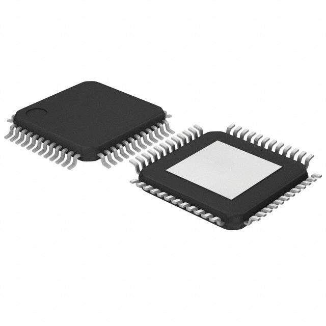
| 产品图片 |
|
| rohs | 符合RoHS无铅 / 符合限制有害物质指令(RoHS)规范要求 |
| 产品系列 | 数据转换器IC,数据转换IC - 各种类型,Analog Devices AD5930YRUZ- |
| 数据手册 | |
| 产品型号 | AD5930YRUZ |
| PCN组件/产地 | |
| 主fclk | 50MHz |
| 产品培训模块 | http://www.digikey.cn/PTM/IndividualPTM.page?site=cn&lang=zhs&ptm=25911http://www.digikey.cn/PTM/IndividualPTM.page?site=cn&lang=zhs&ptm=25920http://www.digikey.cn/PTM/IndividualPTM.page?site=cn&lang=zhs&ptm=25931http://www.digikey.cn/PTM/IndividualPTM.page?site=cn&lang=zhs&ptm=25944http://www.digikey.cn/PTM/IndividualPTM.page?site=cn&lang=zhs&ptm=25943http://www.digikey.cn/PTM/IndividualPTM.page?site=cn&lang=zhs&ptm=25945http://www.digikey.cn/PTM/IndividualPTM.page?site=cn&lang=zhs&ptm=25937 |
| 产品目录页面 | |
| 产品种类 | 数据转换IC - 各种类型 |
| 供应商器件封装 | 20-TSSOP |
| 信噪比 | 60 dB |
| 分辨率 | 10 bit |
| 分辨率(位) | 10 b |
| 功能 | Waveform generator |
| 包装 | 管件 |
| 商标 | Analog Devices |
| 字宽调谐(位) | 24 b |
| 安装类型 | 表面贴装 |
| 安装风格 | SMD/SMT |
| 封装 | Tube |
| 封装/外壳 | 20-TSSOP(0.173",4.40mm 宽) |
| 封装/箱体 | TSSOP-20 |
| 工作温度 | -40°C ~ 125°C |
| 工作温度范围 | - 40 C to + 105 C |
| 工作电源电压 | 2.3 V to 5.5 V |
| 工厂包装数量 | 75 |
| 标准包装 | 1 |
| 电压-电源 | 2.3 V ~ 5.5 V |
| 系列 | AD5930 |
| 视频文件 | http://www.digikey.cn/classic/video.aspx?PlayerID=1364138032001&width=640&height=505&videoID=2245193148001 |
| 转换器数量 | 1 |


.jpg)


- 商务部:美国ITC正式对集成电路等产品启动337调查
- 曝三星4nm工艺存在良率问题 高通将骁龙8 Gen1或转产台积电
- 太阳诱电将投资9.5亿元在常州建新厂生产MLCC 预计2023年完工
- 英特尔发布欧洲新工厂建设计划 深化IDM 2.0 战略
- 台积电先进制程称霸业界 有大客户加持明年业绩稳了
- 达到5530亿美元!SIA预计今年全球半导体销售额将创下新高
- 英特尔拟将自动驾驶子公司Mobileye上市 估值或超500亿美元
- 三星加码芯片和SET,合并消费电子和移动部门,撤换高东真等 CEO
- 三星电子宣布重大人事变动 还合并消费电子和移动部门
- 海关总署:前11个月进口集成电路产品价值2.52万亿元 增长14.8%

PDF Datasheet 数据手册内容提取
Programmable Frequency Sweep and Output Burst Waveform Generator Data Sheet AD5930 FEATURES GENERAL DESCRIPTION Programmable frequency profile The AD59301 is a waveform generator with programmable No external components necessary frequency sweep and output burst capability. Utilizing Output frequency up to 25 MHz embedded digital processing that allows enhanced frequency Burst and listen capability control, the device generates synthesized analog or digital Preprogrammable frequency profile minimizes number of frequency-stepped waveforms. Because frequency profiles DSP/microcontroller writes are preprogrammed, continuous write cycles are eliminated Sinusoidal/triangular/square wave outputs and thereby free up valuable DSP/microcontroller resources. Automatic or single pin control of frequency stepping Waveforms start from a known phase and are incremented Waveform starts at known phase phase continuously, which allows phase shifts to be easily Increments at 0° phase or phase continuously determined. Consuming only 8 mA, the AD5930 provides a Power-down mode: 20 µA convenient low power solution to waveform generation. Power supply: 2.3 V to 5.5 V Automotive temperature range: −40°C to +125°C The AD5930 can be operated in a variety of modes. In 20-lead pb-free TSSOP continuous output mode, the device outputs the required frequency for a defined length of time and then steps to the next frequency. The length of time the device outputs a APPLICATIONS particular frequency is either preprogrammed and the device Frequency sweeping/radar increments the frequency automatically, or, alternatively, is Network/impedance measurements incremented externally via the CTRL pin. In burst mode, the Incremental frequency stimulus device outputs its frequency for a length of time and then Sensory applications returns to midscale for a further predefined length of time Proximity and motion before stepping to the next frequency. When the MSBOUT pin BFSK is enabled, a digital output is generated. Frequency bursting/pulse trains (continued on Page 3) FUNCTIONAL BLOCK DIAGRAM INTERRUPT STANDBY DVDD CAP/2.5V DGND AGND AVDD AD5930 REGULATOR VCC SYNC MCLK 2.5V BUFFER SYNCOUT OUTPUT BURST CONTROLLER DGND O/P DATA SYNC BUFFER MSBOUT CTRL INCREMENT CONTROLLER DATA INCR 24-BIT 10-BIT IOUTB PIPELINED DAC FREQUENCY DDS CORE IOUT CONTROLLER 24 DATA AND CONTROL ON-BOARD FULL-SCALE COMP CONTROL REFERENCE CONTROL SERIAL INTERFACE REGISTER FSYNC SCLK SDATA REF FSADJUST 05333-001 Figure 1. 1 Protected by US Patent Number 6747583. Rev. D Document Feedback Information furnished by Analog Devices is believed to be accurate and reliable. However, no responsibility is assumed by Analog Devices for its use, nor for any infringements of patents or other One Technology Way, P.O. Box 9106, Norwood, MA 02062-9106, U.S.A. rights of third parties that may result from its use. Specifications subject to change without notice. No license is granted by implication or otherwise under any patent or patent rights of Analog Devices. Tel: 781.329.4700 ©2005–2017 Analog Devices, Inc. All rights reserved. Trademarks and registered trademarks are the property of their respective owners. Technical Support www.analog.com
AD5930 Data Sheet TABLE OF CONTENTS Features .............................................................................................. 1 Serial Interface ............................................................................ 17 Applications ....................................................................................... 1 Powering up the AD5930 .......................................................... 17 General Description ......................................................................... 1 Programming the AD5930 ........................................................ 17 Functional Block Diagram .............................................................. 1 Setting up the Frequency Sweep ............................................... 19 Revision History ............................................................................... 2 Activating and Controlling the Sweep ..................................... 20 General Description ......................................................................... 3 Outputs from the AD5930 ........................................................ 21 Specifications ..................................................................................... 4 Applications Information .............................................................. 22 Timing Characteristics ..................................................................... 6 Grounding and Layout .............................................................. 22 Absolute Maximum Ratings ............................................................ 8 AD5930 to ADSP-21467 Interface ........................................... 22 ESD Caution .................................................................................. 8 AD5930 to 68HC11/68L11 Interface ....................................... 23 Pin Configuration and Function Descriptions ............................. 9 AD5930 to 80C51/80L51 Interface .......................................... 23 Typical Performance Characteristics ........................................... 11 AD5930 to DSP56002 Interface ............................................... 23 Terminology .................................................................................... 15 Evaluation Board ........................................................................ 24 Theory of Operation ...................................................................... 16 Schematic..................................................................................... 25 The Frequency Profile ................................................................ 16 Outline Dimensions ....................................................................... 27 Output Modes ............................................................................. 16 Ordering Guide .......................................................................... 27 REVISION HISTORY 5/2017—Rev. C to Rev. D 7/2012—Rev. A to Rev. B Changed µcontroller to Microcontroller ..................... Throughout Change to Ordering Guide ............................................................ 27 Changes to AD5930 to 68HC11/68L11 Interface Section ........ 23 2/2012—Rev. 0 to Rev. A 7/2015—Rev. B to Rev. C Change to Figure 2 ............................................................................ 5 Change to Figure 6 and Figure 7..................................................... 7 Changes to Figure 22, Figure 23, Figure 24, Figure 25, Change to Table 4 ............................................................................. 9 and Figure 26 ................................................................................... 13 Changed Applications Section to Applications Information Changes to Figure 27, Figure 28, Figure 29, and Section and Changed ADSP-2101 to ADSP-21467 .................... 22 Figure 30 .......................................................................................... 25 11/2005—Revision 0: Initial Version Rev. D | Page 2 of 28
Data Sheet AD5930 GENERAL DESCRIPTION (continued from Page 1) sweep again. In addition, a single frequency or burst can be To program the device, the user enters the start frequency, the generated without any sweep. increment step size, the number of increments to be made, and the time interval that the part outputs each frequency. The The AD5930 is written to via a 3-wire serial interface, which frequency sweep profile is initiated, started, and executed by operates at clock rates up to 40 MHz. The device operates with toggling the CTRL pin. a power supply from 2.3 V to 5.5 V. Note that AV and DV DD DD are independent of each other and can be operated from A number of different sweep profiles are offered. Frequencies can different voltages. The AD5930 also has a standby function, be stepped in triangular-sweep mode, which continuously sweeps which allows sections of the device that are not being used up and down through the frequency range. Alternatively, in saw- to be powered down. sweep mode, the frequency is swept up through the frequency range, but returns to the initial frequency before executing the The AD5930 is available in a 20-lead pb-free TSSOP package. Rev. D | Page 3 of 28
AD5930 Data Sheet SPECIFICATIONS AV = DV = 2.3 V to 5.5 V, AGND = DGND = 0 V, T = T to T , R = 6.8 kΩ, R = 200 Ω for IOUT and IOUTB, DD DD A MIN MAX SET LOAD unless otherwise noted. Table 1. Y Grade1 Parameter Min Typ Max Unit Test Conditions/Comments SIGNAL DAC SPECIFICATIONS Resolution 10 Bits Update Rate 50 MSPS I Full-Scale2 3 4.0 mA OUT V Peak-to-Peak 0.56 V OUT V Offset 45 mV From 0 V to the trough of the waveform OUT V 0.325 V Voltage at midscale output MIDSCALE Output Compliance 0.8 V AV = 2.3 V, internal reference used3 DD DC Accuracy Integral Nonlinearity (INL) ±1.5 LSB Differential Nonlinearity (DNL) ±0.75 LSB DDS SPECIFICATIONS Dynamic Specifications Signal-to-Noise Ratio 53 60 dB f = 50 MHz, f = f /4096 MCLK OUT MCLK Total Harmonic Distortion −60 −53 dBc f = 50 MHz, f = f /4096 MCLK OUT MCLK Spurious-Free Dynamic Range (SFDR) Wideband (0 to Nyquist) −62 −52 dBc f = 50 MHz, f = f /50 MCLK OUT MCLK Narrowband (±200 kHz) −76 −73 dBc f = 50 MHz, f = f /50 MCLK OUT MCLK Clock Feedthrough −50 dBc Up to 16 MHz out Wake-Up Time 1.7 ms From standby OUTPUT BUFFER V Peak-to-Peak 0 DV V Typically, square wave on MSBOUT and SYNCOUT OUT DD Output Rise/Fall Time2 12 ns VOLTAGE REFERENCE Internal Reference 1.15 1.18 1.26 V External Reference Range 1.3 V REFOUT Input Impedance 1 kΩ V @ REF pin < Internal V IN REF 25 kΩ V @ REF pin > Internal V IN REF Reference TC2 90 ppm/°C LOGIC INPUTS Input Current 0.1 ±1 µA V , Input High Voltage 1.7 V DV = 2.3 V to 2.7 V INH DD 2.0 V DV = 2.7 V to 3.6 V DD 2.8 V DV = 4.5 V to 5.5 V DD V , Input Low Voltage 0.6 V DV = 2.3 V to 2.7 V INL DD 0.7 V DV = 2.7 V to 3.6 V DD 0.8 V DV = 4.5 V to 5.5 V DD C , Input Capacitance2 3 pF IN LOGIC OUTPUTS2 V , Output High Voltage DV − 0.4 V V I = 1 mA OH DD SINK V , Output Low Voltage 0.4 V I = 1 mA OL SINK Floating-State O/P Capacitance 5 pF Rev. D | Page 4 of 28
Data Sheet AD5930 Y Grade1 Parameter Min Typ Max Unit Test Conditions/Comments POWER REQUIREMENTS f = 50 MHz, f = f /7 MCLK OUT MCLK AV /DV 2.3 5.5 V DD DD I 3.8 4 mA AA I 2.4 2.7 mA DD I + I 6.2 6.7 mA AA DD Low Power Sleep Mode Device is reset before putting into standby 20 85 µA All outputs powered down, MCLK = 0 V, serial interface active 140 240 µA All outputs powered down, MCLK active, serial interface active 1 Operating temperature range is as follows: Y Version: −40°C to +125°C; typical specifications are at 25°C. 2 Guaranteed by design. 3 Minimum RSET = 3.9 kΩ. RSET 100nF 10nF 6.8V CAP/2.5V REFOUT FSADJUST AVDD 10nF REGULATOR ROENF-EBROEANRCDE FUCLOLN-TSRCOALLE COMP AD5930 12 SIN 10-BIT IOUT ROM DAC R20L0OΩAD 20pF 05333-002 Figure 2. Test Circuit Used to Test the Specifications Rev. D | Page 5 of 28
AD5930 Data Sheet TIMING CHARACTERISTICS All input signals are specified with tr = tf = 5 ns (10% to 90% of V ) and timed from a voltage level of (V + V )/2. DD IL IH See Figure 4 to Figure 7. DV = 2.3 V to 5.5 V, AGND = DGND = 0 V, all specifications T to T , unless otherwise noted. DD MIN MAX Table 2.1 Parameter Limit at T , T Unit Conditions/Comments MIN MAX t 20 ns min MCLK period 1 t 8 ns min MCLK high duration 2 t 8 ns min MCLK low duration 3 t 25 ns min SCLK period 4 t 10 ns min SCLK high time 5 t 10 ns min SCLK low time 6 t 5 ns min FSYNC to SCLK falling edge setup time 7 t 10 ns min FSYNC to SCLK hold time 8 t 5 ns min Data setup time 9 t 3 ns min Data hold time 10 t 2 x t ns min Minimum CTRL pulse width 11 1 t 0 ns min CTRL rising edge to MCLK falling edge setup time 12 t 10 x t ns typ CTRL rising edge to IOUT/IOUTB delay (initial pulse, includes initialization) 13 1 8 x t ns typ CTRL rising edge to IOUT/IOUTB delay (initial pulse, includes initialization) 1 t 2 x t ns typ Frequency change to SYNC output, saw sweep, each frequency increment 14 1 t 2 x t ns typ Frequency change to SYNC output, saw sweep, end of sweep 15 1 t 2 x t ns typ Frequency change to SYNC output, triangle sweep, end of sweep 16 1 t 20 ns max MCLK falling edge after 16th clock edge to MSB out 17 1 Guaranteed by design, not production tested. t 1 MCLK t2 t3 05333-003 Figure 3. Master Clock t t 5 4 SCLK t t t 7 6 8 FSYNC t 10 SDATA D15 D14 D2 t9 D1 D0 D15 D14 05333-004 Figure 4. Serial Timing Rev. D | Page 6 of 28
Data Sheet AD5930 t12 MCLK CTRL t11 IOUT/IOUTB t13 05333-005 Figure 5. CTRL Timing CTRL t13 IOUT SYNC O/P (Each Frequency Increment) t14 (End SoYf NSwC eOe/pP) t15 05333-006 Figure 6. CTRL Timing, Saw-Sweep Mode CTRL t13 IOUT SYNC O/P (Each Frequency Increment) t14 (End SoYf SNwC eOe/pP) t16 05333-007 Figure 7. CTRL Timing, Triangular-Sweep Mode Rev. D | Page 7 of 28
AD5930 Data Sheet ABSOLUTE MAXIMUM RATINGS T = 25°C, unless otherwise noted. Stresses at or above those listed under Absolute Maximum A Ratings may cause permanent damage to the product. This is a Table 3. stress rating only; functional operation of the product at these Parameter Rating or any other conditions above those indicated in the operational AVDDto AGND −0.3 V to +6.0 V section of this specification is not implied. Operation beyond DVDD to DGND −0.3 V to +6.0 V the maximum operating conditions for extended periods may AGND to DGND −0.3 V to +0.3 V affect product reliability. CAP/2.5V to DGND −0.3 V to 2.75 V Digital I/O Voltage to DGND −0.3 V to DVDD + 0.3 V ESD CAUTION Analog I/O Voltage to AGND −0.3 V to AVDD + 0.3 V Operating Temperature Range Automotive (Y Version) −40°C to +125°C Storage Temperature Range −65°C to +150°C Maximum Junction Temperature +150°C TSSOP Package (4-Layer Board) θ Thermal Impedance 112°C/W JA θ Thermal Impedance 27.6°C/W JC Reflow Soldering (Pb-Free) 300°C Peak Temperature 260(+0/−5)°C Time at Peak Temperature 10 sec to 40 sec Rev. D | Page 8 of 28
Data Sheet AD5930 PIN CONFIGURATION AND FUNCTION DESCRIPTIONS FSADJUST 1 20 IOUTB REF 2 19 IOUT COMP 3 18 AGND AD5930 AVDD 4 TOP VIEW 17 STANDBY (Not to Scale) DVDD 5 16 FSYNC CAP/2.5V 6 15 SCLK DGND 7 14 SDATA MCLK 8 13 CTRL SYNCOUT 9 12 INTERRUPT MSBOUT 10 11 DGND O/P 05333-008 Figure 8. Pin Configuration Table 4. Pin Function Descriptions Pin No. Mnemonic Description 1 FSADJUST Full-Scale Adjust Control. A resistor (RSET) must be connected externally between this pin and AGND. This determines the magnitude of the full-scale DAC current. The relationship between R and the SET full-scale current is: IOUT = 18 × V /R FULL-SCALE REFOUT SET where V = 1.20 V nominal and R = 6.8 kΩ typical. REFOUT SET 2 REF Voltage Reference. This pin can be an input or an output. The AD5930 has an internal 1.18 V reference, which is made available at this pin. Alternatively, this reference can be overdriven by an external reference, with a voltage range as given in the Specifications section. A 10 nF decoupling capacitor should be connected between REF and AGND. 3 COMP DAC Bias Pin. This pin is used for decoupling the DAC bias voltage to AVDD. 4 AVDD Positive Power Supply for the Analog Section. AVDD can have a value from +2.3 V to +5.5 V. A 0.1 µF decoupling capacitor should be connected between AVDD and AGND. 5 DVDD Positive Power Supply for the Digital Section. DVDD can have a value from +2.3 V to +5.5 V. A 0.1 µF decoupling capacitor should be connected between DVDD and DGND. 6 CAP/2.5V Digital Circuitry. Operates from a 2.5 V power supply. This 2.5 V is generated from DVDD using an on-board regulator. The regulator requires a decoupling capacitor of typically 100 nF, which is connected from CAP/2.5V to DGND. If DVDD is equal to or less than 2.7 V, CAP/2.5V can be shorted to DVDD. 7 DGND Ground for all Digital Circuitry. This excludes digital output buffers. 8 MCLK Digital Clock Input. DDS output frequencies are expressed as a binary fraction of the frequency of MCLK. The output frequency accuracy and phase noise are determined by this clock. 9 SYNCOUT Digital Output for Sweep Status Information. User selectable for end of sweep (EOS) or frequency increments through the control register (SYNCOP bit). This pin must be enabled by setting Control Register Bit SYNCOPEN to 1. 10 MSBOUT Digital Output. The inverted MSB of the DAC data is available at this pin. This output pin must be enabled by setting bit MSBOUTEN in the control register to 1. 11 DGND O/P Separate DGND Connection for Digital Output Buffers. Connect to DGND. 12 INTERRUPT Digital Input. This pins acts as an interrupt during a frequency sweep. A low to high transition is sampled by the internal MCLK, which resets internal state machines. This results in the DAC output going to midscale. 13 CTRL Digital Input. Triple function pin for initialization, start, and external frequency increments. A low-to-high transition, sampled by the internal MCLK, is used to initialize and start internal state machines, which then execute the pre- programmed frequency sweep sequence. When in auto-increment mode, a single pulse executes the entire sweep sequence. When in external increment mode, each frequency increment is triggered by a pulse. 14 SDATA Serial Data Input. The 16-bit serial data-word is applied to this input with the register address first followed by the MSB to LSB of the data. 15 SCLK Serial Clock Input. Data is clocked into the AD5930 on each falling SCLK edge. 16 FSYNC Active Low Control Input. This is the frame synchronization signal for the serial data. When FSYNC is taken low, the internal logic is informed that a new word is being loaded into the device. 17 STANDBY Active High Digital Input. When this pin is high, the internal MCLK is disabled, and the reference DAC and regulator are powered down. For optimum power saving, it is recommended to reset the AD5930 before putting it into standby, as this results in a shutdown current of typically 20 µA. Rev. D | Page 9 of 28
AD5930 Data Sheet Pin No. Mnemonic Description 18 AGND Ground for all Analog Circuitry. 19 IOUT Current Output. This is a high impedance current source output. A load resistor of nominally 200 Ω should be connected between IOUT and AGND. A 20 pF capacitor to AGND is also recommended to act as a low-pass filter and to reduce clock feedthrough. In conjunction with IOUTB, a differential signal is available. 20 IOUTB Current Output. IOUTB is the compliment of IOUT. This pin should preferably be tied through an external load resistor of 200 Ω to AGND, but can be tied directly to AGND. A 20 pF capacitor to AGND is also recommended as a low-pass filter to reduce clock feedthrough. In conjunction with IOUT, a differential signal is available. Rev. D | Page 10 of 28
Data Sheet AD5930 TYPICAL PERFORMANCE CHARACTERISTICS 9 –40 TA = 25°C AVDD = DVDD = 3V/5V 8 AVDD = 5V –45 MCLK = 50MHz MSBOUT, SYNCOUT ENABLED CREG = 011111111111 7 DVDD = 5V –50 TA = 25°C FOUT = MCLK/7 –55 6 I (mA)DD 45 DVDD = 3V SFDR (dBc) –––667050 FOUT = MCLK/50 3 DVDD = 5V, FOUT = MCLK/7 –75 FOUT = MCLK/3 2 –80 10 DVDD = 3V, FOUT = MCLK/7 05333-027 ––8950 05333-030 0 5 10 15 20 25 30 35 40 45 50 0 5 10 15 20 25 30 35 40 45 50 MCLK FREQUENCY (MHz) MCLK FREQUENCY (MHz) Figure 9. Current Consumption (IDD) vs. MCLK Frequency Figure 12. Wideband SFDR vs. MCLK Frequency 7 –60 6 TMAC =L K2 5=° C50MHz SMYSNBCOOUUTT OONN, –65 AMCVRCEDLGDK = == 0 D510V1M1DHD11z =11 31V1/51V1 TA = 25°C 5 MSYSNBCOOUUTT O OFFN, MSBOUT ON, –70 FOUT = MCLK/50 A) 4 SYNCOUT OFF Bc) (mDD 3 DR (d –75 FOUT = MCLK/3 I F S MSBOUT OFF, –80 2 SYNCOUT OFF 10 05333-028 ––8950 FOUT = MCLK/7 05333-031 1kHz 100kHz 1MHz 5MHz 15MHz 25MHz 0 5 10 15 20 25 30 35 40 45 50 500kHz 10kHz 500kHz 2MHz 10MHz 20MHz MCLK FREQUENCY (MHz) FOUT (Hz) Figure 10. IDD vs. FOUT for Various Digital Output Conditions Figure 13. Narrowband SFDR vs. MCLK Frequency –30 3.5 AVDD = DVDD = 3V/5V CREG = 011111111111 3.0 AIDD –40 TA = 25°C MCLK = 50MHz 2.5 –50 DIDD c) A) 2.0 dB I (mDD 1.5 SFDR ( –60 MCLK = 10MHz –70 1.0 MCLK = 1MHz LEGEND MCLK = 30MHz 1. SINEWAVE OUTPUT, INTERNALLY CONTROLLED SWEEP –80 0.05 234... TSTRRINIIAAENNWGGAUUVELLAA ORRU OOTPUUUTTPPT,UU ETTX,, TIENEXTRTENERARNNLAALLYLL LCYYO C CNOOTNRNTOTRRLOLOLELLDLE ESDDW S SEWWEEPEEEPP 05333-029 –900.001 0.01 0.1 1 10 10005333-032 1 2 3 4 CONTROL OPTION (See Legend) FOUT (MHz) Figure 11. IDD vs. Output Waveform Type and Control Figure 14. Wideband SFDR vs. FOUT for Various MCLK Frequencies Rev. D | Page 11 of 28
AD5930 Data Sheet 70 12 TA = 25°C AVDD = DVDD = 5V 65 fOUT = FMCLK/4096 10 S 60 CE 8 VI B) DE R (d 55 OF 6 N R S E B 50 UM 4 N 45 2 40 05333-034 0 05333-025 0 10M 20M 30M 40M 50M 552 554 556 558 560 562 564 566 568 570 572 MCLK FREQUENCY (MHz) VOUT PEAK-TO-PEAK (mV) Figure 15. SNR vs. MCLK Frequency Figure 18. Histogram of VOUT Peak-to-Peak 12 1.25 AVDD = DVDD = 5V 10 1.23 S CE 8 VI E 1.21 D V (V)REF 1.19 UMBER OF 64 N 2 1.17 1.15 05333-035 044.4 44.6 44.8 45.0 45.2 45.4 45.6 45.8 46.0 46.205333-026 –40 –20 0 20 40 60 80 100 120 VOUT OFFSET (mV) TEMPERATURE (°C) Figure 16. VREF vs. Temperature Figure 19. Histogram of VOUT Offset 2.0 0 TA = 25°C 1.9 AVDD = DVDD = 2.3V –10 100mV p-p RIPPLE NO DECOUPLING ON SUPPLIES AVDD = DVDD = 5V 1.8 –20 ME (ms) 1.7 AVDD = DVDD = 5V ON (dB) –30 DVDD (on CAP/2.5V) UP TI 1.6 UATI –40 AKE- 1.5 TTEN –50 W A 1.4 –60 11..32 05333-036 ––7800 AVDD (on IOUT) 05333-033 –40 –20 0 20 40 60 80 100 120 10 100 1k 10k 100k 1M TEMPERATURE (°C) MODULATING FREQUENCY (Hz) Figure 17. Wake-up Time vs. Temperature Figure 20. PSSR Rev. D | Page 12 of 28
Data Sheet AD5930 0 0 –10 –20 –10 –30 –20 –40 –50 –30 –60 E S –70 –40 OI SE N ––8900 (dB) –50 HA –100 –60 P –110 –120 –70 –130 –80 –140 –––111567000 05333-037 –1–0900 05333-016 100 1k 10k 100k 0 5M f (Hz) RWB 1K VWB 300 ST 50 SEC FREQUENCY (Hz) Figure 21. Output Phase Noise Figure 24. f = 10 MHz; f = 3.33 MHz = f /3, MCLK OUT MCLK Frequency Word = 555555 0 0 –10 –10 –20 –20 –30 –30 –40 –40 (dB) –50 (dB) –50 –60 –60 –70 –70 –80 –80 –1–0900 05333-014 –1–0900 05333-017 0 100k 0 160k RWB 100 VWB 30 ST 100 SEC RWB 100 VWB 30 ST 200 SEC FREQUENCY (Hz) FREQUENCY (Hz) Figure 22. fMCLK = 10 MHz; Figure 25. fMCLK = 50 MHz; fOUT = 2.4 kHz, Frequency Word = 000FBA fOUT = 12 kHz, Frequency Word = 000FBA 0 0 –10 –10 –20 –20 –30 –30 –40 –40 dB) –50 dB) –50 ( ( –60 –60 –70 –70 –80 –80 –1–0900 05333-015 –1–0900 05333-018 0 5M 0 1.6M RWB 1K VWB 300 ST 50 SEC RWB 100 VWB 300 ST 200 SEC FREQUENCY (Hz) FREQUENCY (Hz) Figure 23. fMCLK = 10 MHz; Figure 26. fMCLK = 50 MHz; fOUT = 1.43 MHz = fMCLK/7, Frequency Word = 249249 fOUT = 120 kHz, Frequency Word = 009D49 Rev. D | Page 13 of 28
AD5930 Data Sheet 0 0 –10 –10 –20 –20 –30 –30 –40 –40 dB) –50 dB) –50 ( ( –60 –60 –70 –70 –80 –80 –1–0900 05333-019 –1–0900 05333-021 0 25M 0 25M RWB 1K VWB 300 ST 200 SEC RWB 1K VWB 300 ST 200 SEC FREQUENCY (Hz) FREQUENCY (Hz) Figure 27. f = 50 MHz; Figure 29. f = 50 MHz; f = 7.143 MHz = f /7, MCLK MCLK OUT MCLK f = 1.2 MHz, Frequency Word = 0624DD Frequency Word = 2492492 OUT 0 0 –10 –10 –20 –20 –30 –30 –40 –40 (dB) –50 (dB) –50 –60 –60 –70 –70 –80 –80 –1–0900 05333-020 –1–0900 05333-022 0 25M 0 25M RWB 1K VWB 300 ST 200 SEC RWB 1K VWB 300 ST 200 SEC FREQUENCY (Hz) FREQUENCY (Hz) Figure 28. fMCLK = 50 MHz; Figure 30. fMCLK = 50 MHz; fOUT = 16.667 MHz = fMCLK/3, f = 4.8 MHz, Frequency Word = 189374 Frequency Word = 5555555 OUT Rev. D | Page 14 of 28
Data Sheet AD5930 TERMINOLOGY Integral Nonlinearity (INL) Total Harmonic Distortion (THD) This is the maximum deviation of any code from a straight line THD is the ratio of the rms sum of harmonics to the rms value passing through the endpoints of the transfer function. The of the fundamental. For the AD5930, THD is defined as endpoints of the transfer function are zero scale and full scale. V 2 +V 2 +V 2 +V 2 +V 2 The error is expressed in LSBs. THD(dB)=20log 2 3 4 5 6 V Differential Nonlinearity (DNL) 1 This is the difference between the measured and ideal 1 LSB where: change between two adjacent codes in the DAC. A specified V1 is the rms amplitude of the fundamental. differential nonlinearity of ±1 LSB maximum ensures V2, V3, V4, V5, and V6 are the rms amplitudes of the second monotonicity. through the sixth harmonic. Output Compliance Signal-to-Noise Ratio (SNR) The output compliance refers to the maximum voltage that can SNR is the ratio of the rms value of the measured output signal be generated at the output of the DAC to meet the specifica- to the rms sum of all other spectral components below the tions. When voltages greater than that specified for the output Nyquist frequency. The value for SNR is expressed in decibels. compliance are generated, the AD5930 may not meet the Clock Feedthrough specifications listed in the data sheet. There is feedthrough from the MCLK input to the analog Spurious-Free Dynamic Range (SFDR) output. Clock feedthrough refers to the magnitude of the Along with the frequency of interest, harmonics of the MCLK signal relative to the fundamental frequency in the fundamental frequency and images of these frequencies are AD5930’s output spectrum. present at the output of a DDS device. The SFDR refers to the largest spur or harmonic that is present in the band of interest. The wide band SFDR gives the magnitude of the largest harmonic or spur relative to the magnitude of the fundamental frequency in the 0 to Nyquist bandwidth. The narrow band SFDR gives the attenuation of the largest spur or harmonic in a bandwidth of ±200 kHz about the fundamental frequency. Rev. D | Page 15 of 28
AD5930 Data Sheet THEORY OF OPERATION The AD5930 is a general-purpose synthesized waveform Triangular-Sweep Mode generator capable of providing digitally programmable In the case of a triangular sweep, the AD5930 repeatedly waveform sequences in both the frequency and time domain. sweeps between sweep start to sweep end, that is, from F START The device contains embedded digital processing to provide a incrementally to repetitive sweep of a user programmable frequency profile F + N × Δf allowing enhanced frequency control. Because the device is pre- START INCR programmable, it eliminates continuous write cycles from a and then returns to FSTART in a decremented manner (see DSP/μcontroller in generating a particular waveform. Figure 32). The triangular-sweep cycle time is given by THE FREQUENCY PROFILE (1 + (2 × N )) × t The frequency profile is defined by the start frequency (F ), INCR INT START the frequency increment (Δf) and the number of increments per sweep (N ). The increment interval between frequency INCR increments, t , is either user programmable with the interval INT automatically determined by the device (auto-increment mode), FSTART or externally controlled via a hardware pin (external increment MIDSCALE mforo da ef)ix. eFdo rn auumtobmera toifc culopcdka tpee, rtihoed isn oterr fvoarl ap rfioxfeilde ncaunm ebiethr eorf be FSTART FSTART +ΔFFSTART + NINCR ×FΔSTFART +ΔF FSTART 05333-010 output waveform cycles. Figure 32. Triangular-Sweep Profile OUTPUT MODES In the auto-increment mode, a single pulse at the CTRL pin starts and executes the frequency sweep. In the external increment The AD5930 offers two possible output modes: continuous mode, the CTRL pin also starts the sweep, but the frequency output mode and burst output mode. Both of these modes are increment interval is determined by the time interval between illustrated in Figure 33. sequential 0/1 transitions on the CTRL pin. Furthermore, the CTRL pin can be used to directly control the burst profile, where tINT during the input high time, the output waveform is present, and CONTINUOUS during the input low time, the output is reset to midscale. MODE The frequency profile can be swept in two different modes: saw TBURST sweep or triangular (up/down) sweep. BURST MODE Saw-Sweep Mode Isnw ethepe sc baseetw oef ean s aswwe sewpe setpa,r tt htoe AswDe5e9p3 e0n rde,p tehaatte idsl,y f r om NU1MBER STEP CHANG2ES 05333-011 FSTART incrementally to Figure 33. Continuous Mode and Burst Mode of the AD5930 FSTART + NINCR × Δf Continuous Output Mode and then returns directly to F to begin again (see Figure 31). START In this mode, each frequency of the sweep is available for the This gives a saw-sweep cycle time of length of time programmed into the time interval (tINT) register. This means the frequency swept output signal is continuously (N + 1) × t INCR INT available, and is therefore phase continuous at all frequency increments. To set up the AD5930 in continuous mode, the CW/BURST bit (D7) in the control register must be set to 0. See the Activating and Controlling the Sweep section for more details. Burst Output Mode FSTART In this mode, the AD5930 provides a programmable burst MIDSCALE of the waveform output for a fixed length of time (T ) BURST FSTART FSTART + ΔF FSTART + NINCR ×ΔF 05333-009 twhieth rienm tahien pdreor gorfa tmhem ted iinncterermvael,n tth ien toeurtvpaul t( tiIsN rTe).s eTth teon for INT Figure 31. Saw-Sweep Profile Rev. D | Page 16 of 28
Data Sheet AD5930 mid-scale and remains there until the next frequency PROGRAMMING THE AD5930 increment. This is beneficial for applications where the user The AD5930 is designed to provide automatic frequency sweeps needs to burst a frequency for a set period, and then “listen” for when the CTRL pin is triggered. The automatic sweep is a response before increasing to the next frequency. Note also controlled by a set of registers, the addresses of which are given that the beginning of each frequency increment is at midscale in Table 5. The function of each register is described in more (Phase 0 Rad). Therefore, the phase of the signal is always detail in the following section. known. Table 5. Register Addresses To set up the AD5930 in burst mode, the CW/BURST bit (D7) Register Address in the control register must be set to 1. See the Activating and D15 D14 D13 D12 Mnemonic Name Controlling the Sweep section for more details about the burst 0 0 0 0 C Control bits REG output mode. 0 0 0 1 N Number of INCR increments SERIAL INTERFACE 0 0 1 0 ∆f Lower 12 bits of delta The AD5930 has a standard 3-wire serial interface, which is frequency compatible with SPI®, QSPI™, MICROWIRE™, and DSP 0 0 1 1 ∆f Higher 12 bits of delta frequency interface standards. 0 1 t Increment interval INT Data is loaded into the device as a 16-bit word under the 1 0 T Burst interval BURST control of a serial clock input, SCLK. The timing diagram for 1 1 0 0 F Lower 12 bits of start START this operation is given in Figure 4. frequency 1 1 0 1 F Higher 12 bits of start START The FSYNC input is a level-triggered input that acts as a frame frequency synchronization and chip enable. Data can only be transferred 1 1 1 0 Reserved into the device when FSYNC is low. To start the serial data 1 1 1 1 Reserved transfer, FSYNC should be taken low, observing the minimum FSYNC to SCLK falling edge setup time, t. After FSYNC goes 7 The Control Register low, serial data is shifted into the device's input shift register on The AD5930 contains a 12-bit control register (see Table 6) that the falling edges of SCLK for 16 clock pulses. FSYNC can be taken high after the 16th falling edge of SCLK, observing the sets up the operating modes of the AD5930. The different functions and the various output options from the AD5930 are minimum SCLK falling edge to FSYNC rising edge time, t 8. controlled by this register. Table 7 describes the individual bits Alternatively, FSYNC can be kept low for a multiple of 16 SCLK of the control register. pulses, and then brought high at the end of the data transfer. In this way, a continuous stream of 16-bit words can be loaded while To address the control register, D15 to D12 of the 16-bit serial FSYNC is held low. FSYNC should only go high after the 16th word must be set to 0. SCLK falling edge of the last word is loaded. Table 6. Control Register The SCLK can be continuous, or, alternatively, the SCLK can D15 D14 D13 D12 D11 to D0 idle high or low between write operations. 0 0 0 0 Control Bits POWERING UP THE AD5930 When the AD5930 is powered up, the part is in an undefined state, and therefore, must be reset before use. The eight registers (control and frequency) contain invalid data and need to be set to a known value by the user. The control register should be the first register to be programmed, as this sets up the part. Note that a write to the control register automatically resets the internal state machines and provides an analog output of midscale as it provides the same function as the INTERRUPT pin. Typically, this is followed by a serial loading of all the required sweep parameters. The DAC output remains at midscale until a sweep is started using the CTRL pin. Rev. D | Page 17 of 28
AD5930 Data Sheet Table 7. Description of Bits in the Control Register Bit Name Function D15 ADDR Register address bits. to D12 D11 B24 Two write operations are required to load a complete word into the F register and the Δf register. START When B24 = 1, a complete word is loaded into a frequency register in two consecutive writes. The first write contains the 12 LSBs of the frequency word and the next write contains the 12 MSBs. Refer to Table 5 for the appropriate addresses. The write to the destination register occurs after both words have been loaded, so the register never holds an intermediate value. When B24 = 0, the 24-bit F /Δf register operates as two 12-bit registers, one containing the 12 MSBs and the START other containing the 12 LSBs. This means that the 12 MSBs of the frequency word can be altered independent of the 12 LSBs and vice versa. This is useful if the complete 24-bit update is not required. To alter the 12 MSBs or the 12 LSBs, a single write is made to the appropriate register address. Refer to Table 5 for the appropriate addresses. D10 DAC ENABLE When DAC ENABLE = 1, the DAC is enabled. When DAC ENABLE = 0, the DAC is powered down. This saves power and is beneficial when only using the MSB of the DAC input data (available at the MSBOUT pin). D9 SINE/TRI The function of this bit is to control what is available at the IOUT/IOUTB pins. When SINE/TRI = 1, the SIN ROM is used to convert the phase information into amplitude information resulting in a sinusoidal signal at the output. When SINE/TRI = 0, the SIN ROM is bypassed, resulting in a triangular (up-down) output from the DAC. D8 MSBOUTEN When MSBOUTEN = 1, the MSBOUT pin is enabled. When MSBOUTEN = 0, the MSBOUT is disabled (tri-state). D7 CW/BURST When CW/BURST = 1, the AD5930 outputs each frequency continuously for the length of time or number of output waveform cycles specified in the appropriate register, T . BURST When CW/BURST = 0, the AD5930 bursts each frequency for the length of time/number of cycles specified in the burst register, TBURST. For the remainder of the time within each increment window (TBURST − tINT), the AD5930 outputs a DC value of midscale. In external increment mode, it is defined by the pulse widths on the CTRL pin. D6 INT/EXT This bit is active when D7 = 0 and is also used in conjunction with D5. When the user is incrementing the frequency BURST externally (D5 = 1), D6 dictates whether the user is controlling the burst internally or externally. When INT/EXT BURST = 1, the output burst is controlled externally through the CTRL pin. This is useful if the user is using an external source to both trigger the frequency increments and determine the burst interval. When INT/EXT BURST = 0, the output burst is controlled internally. The burst is pre-programmed by the user into the T register (the burst interval can either be clock-based or for a specified number of output cycles). BURST When D5 = 0, this bit is ignored. D5 INT/EXT When INT/EXT INCR = 1, the frequency increments are triggered externally through the CTRL pin. INCR When INT/EXT INCR = 0, the frequency increments are triggered automatically. D4 MODE The function of this bit is to control what type of frequency sweep is carried out. When MODE = 1, the frequency profile is a saw sweep. When MODE = 0, the frequency profile is a triangular (up-down) sweep. D3 SYNCSEL This bit is active when D2 = 1. It is user-selectable to pulse at the end of sweep (EOS) or at each frequency increment. When SYNCSEL = 1, the SYNCOP pin outputs a high level at the end of the sweep and returns to zero at the start of the subsequent sweep. When SYNCSEL= 0, the SYNCOP outputs a pulse of 4 × T only at each frequency increment. CLOCK D2 SYNCOUTEN When SYNCOUTEN= 1, the SYNC output is available at the SYNCOP pin. When SYNCOUTEN= 0, the SYNCOP pin is disabled (tri-state). D1 Reserved This bit must always be set to 1. D0 Reserved This bit must always be set to 1. Rev. D | Page 18 of 28
Data Sheet AD5930 SETTING UP THE FREQUENCY SWEEP Number of Increments (N ) INCR As stated previously in The Frequency Profile section, the An end frequency, or a maximum/minimum frequency before AD5930 requires certain registers to be programmed to enable a the sweep changes direction is not required on the AD5930. frequency sweep. The following sections discuss these registers Instead, this end frequency is calculated by multiplying the in more detail. frequency increment value (Δf) by the number of frequency steps (N ), and adding it to/subtracting it from the start INCR Start Frequency (F ) START frequency (F ), that is, F + N × Δf. The N register START START INCR INCR To start a frequency sweep, the user needs to tell the AD5930 is a 12-bit register, with the address shown in Table 10. what frequency to start sweeping from. This frequency is stored Table 10. N Register Bits INCR in a 24-bit register called F . If the user wishes to alter the START D15 D14 D13 D12 D11 to D0 entire contents of the F register, two consecutive writes START 0 0 0 1 12 bits of N <11…0> INCR must be performed, one to the LSBs and the other to the MSBs. Note that for an entire write to this register, the Control Bit B24 The number of increments is programmed in binary fashion, (D11) should be set to 1 with the LSBs programmed first. with 000000000010 representing the minimum number of frequency increments (2 increments), and 111111111111 In some applications, the user does not need to alter all 24 bits representing the maximum number of increments (4095). of the F register. By setting the Control Bit B24 (D11) to 0, START Table 11. N Data Bits the 24-bit register operates as two 12-bit registers, one INCR D11 D0 Number of Increments containing the 12 MSBs and the other containing the 12 LSBs. 0000 0000 0010 2 frequency increments. This is the This means that the 12 MSBs of the F word can be altered START minimum number of frequency independently of the 12 LSBs, and vice versa. The addresses of increments. both the LSBs and the MSBs of this register is given in Table 8. 0000 0000 0011 3 frequency increments. Table 8. F Register Bits 0000 0000 0100 4 frequency increments. START D15 D14 D13 D12 D11 to D0 … … … … 1 1 0 0 12 LSBs of F <11…0> 1111 1111 1110 4094 frequency increments. START 1 1 0 1 12 MSBs of F <23…12> 1111 1111 1111 4095 frequency increments. START Frequency Increments (∆f) Increment Interval (tINT) The value in the Δf register sets the increment frequency for the The increment interval dictates the duration of the DAC output sweep and is added incrementally to the current output frequency. signal for each individual frequency of the frequency sweep. Note that the increment frequency can be positive or negative, The AD5930 offers the user two choices: thereby giving an increasing or decreasing frequency sweep. • The duration is a multiple of cycles of the output frequency. At the start of a sweep, the frequency contained in the F START • The duration is a multiple of MCLK periods. register is output. Next, the frequency (F + Δf ) is output. START This is followed by (FSTART + Δf + Δf) and so on. Multiplying the This is selected by Bit D13 in the tINT register as shown in Table 12. Δf value by the number of increments (N ), and adding it to INCR Table 12. t Register Bits the start frequency (F ), gives the final frequency in the INT START D15 D14 D13 D12 D11 D10 to D0 sweep. Mathematically this final frequency/stop frequency is 0 1 0 x x 11 bits <10…0> represented by Fixed number of output F + (N × Δf). waveform cycles. START INCR 0 1 1 x x 11 bits <10…0> The Δf register is a 23-bit register, and requires two 16-bit Fixed number of clock writes to be programmed. Table 9 gives the addresses associated periods. with both the MSB and LSB registers of the Δf word. Programming of this register is in binary form with the Table 9. ∆f Register Bits minimum number being decimal 2. Note in Table 12 that 11 Sweep bits, Bit D10 to Bit D0, of the register are available to program D15 D14 D13 D12 D11 D10 to D0 Direction the time interval. As an example, if MCLK = 50 MHz, then each 0 0 1 0 12 LSBs of ∆f N/A clock period/base interval is (1/50 MHz) = 20 ns. If each <11…0> frequency needs to be output for 100 ns, then <00000000101> 0 0 1 1 0 11 MSBs of Positive Δf or decimal 5 needs to be programmed to this register. Note that Δf <22…12> (FSTART + Δf) the AD5930 can output each frequency for a maximum 0 0 1 1 1 11 MSBs of Negative ∆f duration of 211 −1 (or 2047) times the increment interval. Δf <22…12> (FSTART − Δf) Rev. D | Page 19 of 28
AD5930 Data Sheet Therefore, in this example, a time interval of 20 ns × 2047 = 40 µs Table 14. T Register Bits BURST is the maximum, with the minimum being 40 ns. For some D15 D14 D13 D12 D11 D10 to D0 applications, this maximum time of 40 µs may be insufficient. 1 0 0 x x 11 bits of <0…10> Therefore, to cater for sweeps that need a longer increment Fixed number of output waveform cycles. interval, time-base multipliers are provided. Bit D12 and Bit D11 1 0 1 x x 11 bits of <0…10> are dedicated to the time-base multipliers (see Table 12). A more Fixed number of clock detailed table of the multiplier options is given in Table 13. periods. Table 13. Time-Base Multiplier Values However, note that when using both the increment interval D12 D11 Multiplier Value (t ) and burst time register (T ), the settings for Bit D13 INT BURST 0 0 Multiply (1/MCLK) by 1 should be the same. In instances where they differ, the AD5930 0 1 Multiply (1/MCLK) by 5 defaults to the value programmed into the t register. INT 1 0 Multiply (1/MCLK) by 100 Similarly, Bit 12 and Bit 11, the time-base multiplier bits, always 1 1 Multiply (1/MCLK) by 500 default to the value programmed into the t register. INT If MCLK is 50 MHz and a multiplier of 500 is used, then the ACTIVATING AND CONTROLLING THE SWEEP base interval (T ) is now (1/(50 MHz) x 500)) = 10 µs. Using BASE a multiplier of 500, the maximum increment interval is 10 µs × After the registers have been programmed, a 0 ≥ 1 transition on 211 − 1 = 20.5 ms. Therefore, the option of time-base multipliers the CTRL pin starts the sweep. The sweep always starts from gives the user enhanced flexibility when programming the the frequency programmed into the FSTART register. It changes by length of the frequency window, because any frequency can be the value in the ∆F register and increases by the number of output for a minimum of 40 ns up to a maximum of 20.5 ms. steps in the N register. However, both the time interval and INCR burst duration of each frequency can be internally controlled Length of Sweep Time using the t and T registers, or externally using the CTRL INT BURST The length of time to complete a user-programmed frequency pin. The options available are: sweep is given by the following equation: • Auto-increment, auto-burst control T = (1 + N ) × T SWEEP INCR BASE • External increment, auto-burst control Burst Time Resister (T ) BURST • External increment, external burst control As previously described in the Burst Output Mode section, the Auto-Increment, Auto-Burst Control AD5930 offers the user the ability to output each frequency in the sweep for a length of time within the increment interval The values in the t and T registers are used to control the INT BURST (tINT), and then return to midscale for the remainder of the time sweep. The AD5930 bursts each frequency for the length of (tINT – TBURST) before stepping to the next frequency. The burst time programmed in the TBURST register, and outputs midscale option must be enabled. This is done by setting Bit D7 in the for the remainder of the interval time (t – T ). INT BURST control register to 0. To set up the AD5930 to this mode, CW/BURST (Bit D7) in the Similar to the time interval register, the burst register can have control register must be set to 0, INT/EXT BURST (Bit D6) its duration as: must be set to 0, and INT/EXT INCR (Bit D5) must be set to 0. Note that if the part is only operating in continuous mode, then • A multiple of cycles of the output frequency (Bit D7) in the control register should be set to 1. • A multiple of MCLK periods External Increment, Auto-Burst Control The address for this register is given in Table 14. The time interval, t , is set by the pulse rate on the CTRL pin. INT The first 0 ≥1 transition on the pin starts the sweep. Each subsequent 0 ≥1 transition on the CTRL pin increments the output frequency by the value programmed into the ∆F register. For each increment interval, the AD5930 outputs each frequency for the length of time programmed into the T BURST register, and outputs midscale until the CTRL pin is pulsed again. Note that for this mode, the values programmed into Bit D13, Bit D12, and bit D11 of the T register are used. BURST Rev. D | Page 20 of 28
Data Sheet AD5930 To setup the AD5930 to this mode, CW/BURST (Bit D7) in the OUTPUTS FROM THE AD5930 control register must be set to 0, INT/EXT BURST (Bit D6) The AD5930 offers a variety of outputs from the chip. The analog must be set to 0, and INT/EXT INCR (Bit D5) must be set to 1. outputs are available from the IOUT/IOUTB pins, and include a Note that if the part is only operating in continuous mode, then sine wave and a triangle output. The digital outputs are available Bit D7 in the control register should be set to 1. from the MSBOUT pin and the SYNCOUT pin. External Increment, External Burst Control Analog Outputs Both the increment interval (t ) and the burst interval (T ) INT BURST Sinusoidal Output are controlled by the CTRL pin. A 0 ≥ 1 transition on the CTRL The SIN ROM is used to convert the phase information from pin starts the sweep. The duration of CTRL high then dictates the frequency register into amplitude information, which results the length of time the AD5930 bursts that frequency. The low in a sinusoidal signal at the output. To have a sinusoidal output time of CTRL is the “listen” time, that is, how long the part from the IOUT/IOUTB pins, set Bit SINE/TRI (Bit D9) to 1. remains at midscale. Bringing the CTRL pin high again initiates a frequency increment, and the pattern continues. For this mode, Triangle Output the settings for Bit D13, Bit D12, and Bit D11 are ignored. The SIN ROM can be bypassed so that the truncated digital To setup the AD5930 to this mode, CW/BURST (Bit D7) in the output from the NCO is sent to the DAC. In this case, the control register must be set to 0, INT/EXT BURST (Bit D6) output is no longer sinusoidal. The DAC produces a 10-bit must be set to 1, and INT/EXT INCR (Bit D5) must be set to 1. linear triangular function. To have a triangle output from the Note that if the part is only operating in continuous mode, then IOUT/IOUTB pins, set Bit SINE/TRI (D9) to 0. Note that the Bit D7 in the control register should be set to 1. DAC ENABLE bit (D10) must be 1 (that is, the DAC is enabled) when using these pins. Interrupt Pin This function is used as an interrupt during a frequency sweep. VOUT MAX p/2 5p/2 9p/2 A low-to-high transition on this pin is sampled by the internal Min CthLeK o, uthtpeuret bgyo irnegse ttoti nmgi dinsctearlne.a l state machines, which results VOUT MIN 3p/2 7p/2 11p/2 05333-012 Figure 34. Triangle Output Standby Pin Digital Outputs Sections of the AD5930 that are not in use can be powered Square Wave Output from MSBOUT down to minimize power consumption. This is done by using the STANDBY pin. For the optimum power savings, it is The inverse of the MSB from the NCO can be output from the recommended to reset the AD5930 before entering standby, AD5930. By setting the MSBOUTEN (D8) control bit to 1, the because doing so reduces the power-down current to 20 μA. inverted MSB of the DAC data is available at the MSBOUT pin. This is useful as a digital clock source. When this pin is high, the internal MCLK is disabled, and the reference, DAC, and regulator are powered down. When in this DVDD svtaaltuee, tahse t hDeA NCC oOu tipsu nto o lfo tnhgee Ar Dac5c9u3m0 urleamtinaign. sW ath ietsn pthrees ednetv ice DGND 05333-013 is taken back out of standby mode, the MCLK is re-activated Figure 35. MSB Output and the sweep continues. To ensure correct operation for new SYNCOUT Pin data, it is recommended that the device be internally reset using a control register write or using the INTERRUPT pin, and then The SYNCOUT pin can be used to give the status of the sweep. restarted. It is user selectable for the end of the sweep, or to output a 4 × T pulse at frequency increments. The timing information CLOCK for both of these modes is shown in Figure 6 and Figure 7. The SYNCOUT pin must be enabled before use. This is done using Bit D2 in the control register. The output available from this pin is then controlled by Bit D3 in the control register. See Table 5 for more information. Rev. D | Page 21 of 28
AD5930 Data Sheet APPLICATIONS INFORMATION GROUNDING AND LAYOUT Proper operation of the comparator requires good layout strategy. The strategy must minimize the parasitic capacitance The printed circuit board that houses the AD5930 should be between V and the SIGN BIT OUT pin by adding isolation designed so that the analog and digital sections are separated IN using a ground plane. For example, in a multilayered board, the and confined to certain areas of the board. This facilitates the V signal could be connected to the top layer and the SIGN use of ground planes that can be easily separated. A minimum IN BIT OUT connected to the bottom layer, so that isolation is etch technique is generally best for ground planes because it provided between the power and ground planes. gives the best shielding. Digital and analog ground planes should only be joined in one place. If the AD5930 is the only Interfacing to Microprocessors device requiring an AGND to DGND connection, then the The AD5930 has a standard serial interface that allows the part ground planes should be connected at the AGND and DGND to interface directly with several microprocessors. The device pins of the AD5930. If the AD5930 is in a system where uses an external serial clock to write the data/control multiple devices require AGND to DGND connections, the information into the device. The serial clock can have a connection should be made at one point only, a star ground frequency of 40 MHz maximum. The serial clock can be point that should be established as close as possible to the continuous, or it can idle high or low between write operations. AD5930. When data/control information is being written to the AD5930, Avoid running digital lines under the device as these couple FSYNC is taken low and is held low while the 16 bits of data are noise onto the die. The analog ground plane should be allowed being written into the AD5930. The FSYNC signal frames the to run under the AD5930 to avoid noise coupling. The power 16 bits of information being loaded into the AD5930. supply lines to the AD5930 should use as large a track as AD5930 TO ADSP-21467 INTERFACE possible to provide low impedance paths and reduce the effects of glitches on the power supply line. Fast switching signals, such Figure 36 shows the serial interface between the AD5930 and as clocks, should be shielded with digital ground to avoid the ADSP-21467. The ADSP-21467 should be set up to operate radiating noise to other sections of the board. Avoid crossover in the SPORT transmit alternate framing mode (TFSW = 1). of digital and analog signals. Traces on opposite sides of the The ADSP-21467 is programmed through the SPORT control board should run at right angles to each other. This reduces the register and should be configured as follows: effects of feedthrough through the board. A microstrip 1. Internal clock operation (ISCLK = 1) technique is by far the best, but is not always possible with a 2. Active low framing (INVTFS = 1) double-sided board. In this technique, the component side of the board is dedicated to ground planes, while signals are placed 3. 16-bit word length (SLEN = 15) on the other side. 4. Internal frame sync signal (ITFS = 1) Good decoupling is important. The analog and digital supplies 5. Generate a frame sync for each write (TFSR = 1) to the AD5930 are independent and separately pinned out to Transmission is initiated by writing a word to the Tx register minimize coupling between analog and digital sections of the after the SPORT has been enabled. The data is clocked out on device. All analog and digital supplies should be decoupled to each rising edge of the serial clock and clocked into the AD5930 AGND and DGND, respectively, with 0.1 µF ceramic capacitors on the SCLK falling edge. in parallel with 10 µF tantalum capacitors. To achieve the best from the decoupling capacitors, they should be placed as close ADSP-214671 AD59301 as possible to the device, ideally right up against the device. In systems where a common supply is used to drive both the AVDD and DVDD of the AD5930, it is recommended that the TFS FSYNC system’s AVDD supply be used. This supply should have the DT SDATA recommended analog supply decoupling between the AVDD SCLK SCLK pins of the AD5930 and AGND, and the recommended digital sDuGppNlyD d. ecoupling capacitors between the DVDD pins and 1ADDITIONAL PINS OMITTED FOR CLARITY. 05333-038 Figure 36. ADSP-21467 to AD5930 Interface Rev. D | Page 22 of 28
Data Sheet AD5930 AD5930 TO 68HC11/68L11 INTERFACE is initiated to transmit the second byte of data. P3.3 is taken high following the completion of the second write operation. Figure 37 shows the serial interface between the AD5930 and SCLK should idle high between the two write operations. The the 68HC11/68L11 microcontroller. The microcontroller is 80C51/80L51 outputs the serial data in an LSB first format. The configured as the master by setting bit MSTR in the SPCR to 1, AD5930 accepts the MSB first (the 4 MSBs being the control which provides a serial clock on SCK while the MOSI output information, the next 4 bits being the address while the 8 LSBs drives the serial data line SDATA. Since the microcontroller contain the data when writing to a destination register). does not have a dedicated frame sync pin, the FSYNC signal is Therefore, the transmit routine of the 80C51/80L51 must take derived from a port line (PC7). The setup conditions for correct this into account and rearrange the bits so that the MSB is operation of the interface are as follows: output first. 1. SCK idles high between write operations (CPOL = 1) 2. Data is valid on the SCK falling edge (CPHA = 0) 80C51/80L511 AD59301 When data is being transmitted to the AD5930, the FSYNC line is taken low (PC7). Serial data from the 68HC11/68L11 is P3.3 FSYNC RXD SDATA transmitted in 8-bit bytes with only eight falling clock edges TXD SCLK occurring in the transmit cycle. Data is transmitted MSB first. Ifinr sotr 8d ebri ttso a lroea tdr adnastfae rinretdo tahned A aD se5c9o3n0d, PseCr7ia ils w hreiltde loopwe raafttieorn t hise 05333-040 1ADDITIONAL PINS OMITTED FOR CLARITY. performed to the AD5930. Only after the second 8 bits have Figure 38. 80C51/80L51 to AD5930 Interface been transferred should FSYNC be taken high again. AD5930 TO DSP56002 INTERFACE 68HC11/68L111 AD59301 Figure 39 shows the interface between the AD5930 and the DSP56002. The DSP56002 is configured for normal mode, PC7 FSYNC asynchronous operation with a gated internal clock (SYN = 0, MOSI SDATA GCK = 1, SCKD = 1). The frame sync pin is generated internally SCK SCLK (SC2 = 1), the transfers are 16 bits wide (WL1 = 1, WL0 = 0), and 05333-039 sthyen cfr saimgnea sly ins ca vsiaginlaabl lfer aomn ePsi nth SeC 126, bbiutst (nFeSeLd =s t0o) .b Te hinev ferratmede 1ADDITIONAL PINS OMITTED FOR CLARITY. before being applied to the AD5930. The interface to the Figure 37. 68HC11/68L11 to AD5930 Interface DSP56000/DSP56001 is similar to that of the DSP56002. AD5930 TO 80C51/80L51 INTERFACE Figure 38 shows the serial interface between the AD5930 and DSP560021 AD59301 the 80C51/80L51 microcontroller. The microcontroller is operated in mode 0 so that TXD of the 80C51/80L51 drives SC2 FSYNC SCLK of the AD5930, while RXD drives the serial data line STD SDATA SDATA. The FSYNC signal is again derived from a bit SCK SCLK pdriaoggrraamm)m. Wabhlee np idna otan itsh teo pboer ttr (aPn3s.m3 ibtteeindg t ou sthede AinD th59e 30, P3.3 05333-041 is taken low. The 80C51/80L51 transmits data in 8-bit bytes, 1ADDITIONAL PINS OMITTED FOR CLARITY. thus, only eight falling SCLK edges occur in each cycle. To load Figure 39. DSP56002 to AD5930 Interface the remaining 8 bits to the AD5930, P3.3 is held low after the first 8 bits have been transmitted, and a second write operation Rev. D | Page 23 of 28
AD5930 Data Sheet EVALUATION BOARD Using the AD5930 Evaluation Board The AD5930 evaluation board allows designers to evaluate the The AD5930 evaluation kit is a test system designed to simplify high performance AD5930 DDS modulator with minimum the evaluation of the AD5930. An application note is also effort. available with the evaluation board and gives full information on operating the evaluation board. The evaluation board interfaces to the USB port of a PC. It is Prototyping Area possible to power the entire board off the USB port. All that is needed to complete the evaluation of the chip is either a An area is available on the evaluation board for the user to add spectrum analyzer or a scope. additional circuits to the evaluation test set. Users may want to build custom analog filters for the output or add buffers and The DDS evaluation kit includes a populated and tested operational amplifiers to be used in the final application. AD5930 printed circuit board. The EVAL-AD5930EB kit is shipped with a CD-ROM that includes self-installing software. XO vs. External Clock The PC is connected to the evaluation board using the supplied The AD5930 can operate with master clocks up to 50 MHz. A cable. The software is compatible with Microsoft® Windows® 50 MHz oscillator is included on the evaluation board. 2000 and Windows XP. However, this oscillator can be removed and, if required, an external CMOS clock can be connected to the part. A schematic of the evaluation board is shown in Figure 40 and Figure 41. Rev. D | Page 24 of 28
Data Sheet AD5930 SCHEMATIC V R12.2kΩR0603 3 3. R22.2kΩR0603 V 3 3. C1110µFRTAJ_A + C622pFC0603 8VCC7WP6SCL5SDA CL F03 4LC01 A0A1A2VSS SDAS C222pC06 3.3V 2 1234 Y1 24MHz C122pFC0603 8901234556789012 901 65 1122222244444555 233 11 4 5 3.3V R17C100Ω2.2µFR0603RTAJ_A + 3.3V C70.1µFC060377235131712345 CCCCCCCCCCCCCCCCPB0/FD0VVVVVVVVAPB1/FD1PB2/FD242RESETPB3/FD344PB4/FD4*WAKEUPPB5/FD5PB6/FD654PB7/FD7CLKOUTPD0/FD8PD1/FD9U49D–PD2/FD10CY7C68013-CSP8PD3/FD11D+PD4/FD12PD5/FD1333PA0/INT0PD6/FD1434PA1/INT1PD7/FD1535PA2/*SLOE36PA3/*WU237CTL0/*FLAGAPA4/FIFOADR038CTL1/*FLAGBPA5/FIFOADR139CTL2/*FLAGCPA6/*PKTEND40PA7/*FLD/SLCS SDA1RDY0/*SLRDSCL2RDY1/*SLWR 13IFCLKXTALOUT14RSVDXTALINDNDDDDDDDNNNNNNNGGGGGGGGA 620681361122455 V R17100kΩR0603 C40.1µFC0603 ANDBYRRUPTCTRLSDATASCLKFSYNC 3 TE 3. SNT V R4100kΩR0603 C30.1µFC0603 I 3 C120.1µFC0603 3. 3.3V C50.1µFC0603 1263 3303-3.3 VCCWPSCLNRGND4U3 C360.1µF ADP IN1IN2SD F 875 C350.1µ 02AK LED C80.1µFC0603 C340.1µF T7 R31kΩR0603 C9+10µFRTAJ_A C33C320.1µF0.1µF 3.3V 5 T6 T F 12345 C300.1µ GL22 ND LINK J1 USB-MINI-B VBUSD–D+IOGND 3.3V C280.1µF T3T4 U 1 O D R L G SHIE 05333-023 Figure 40. Page 1 of EVAL-AD5930EB Schematic Rev. D | Page 25 of 28
AD5930 Data Sheet REF C22J150.1µFC0603 IOUT R7J11200ΩR0603 IOUTB R8J12200ΩR0603 MSBOUT C26J10C0603 SYNCOUT C18J9C0603 REF C24C0603 C25C0603 MSBOUT SYNCOUT T24 IOUT IOUTB 3 2 T D D AVDD J14–1 AGND J14–2 R66.8kΩR0603 AV R163.3VLK8L1LK11.5kΩ BAAB21BEAD AVDDDVDD C14C13C31C290.1µF10µF0.1µF10µFC0603RTAJ_AC0603RTAJ_A C1610µFRTAJ_ADVDD+ C15AVDD0.1µFC19C060310µFRTAJ_A +T26FS_ALK7C17C200.1µF0.1µFC0603C0603C21C0603654 CAP/2.5VDVDDAVDD161C23FSYNCFSADJUST0.01µF152SCLKREFC0603143SDATACOMPU1AD59301319CTRLIOUT1220INTERRUPTIOUTB17STANDBY10MSBOUT98SYNCOUTMCLK DGND O/PDGNDAGND 17811SURFACE MOUNTAREATHROUGH HOLEAREAGL1MCLKGROUND LINK DVDD J2–1 DGND J2–2 FSYNC K DVDD SCLA C170.1µFC0603 T A SD 25 T 4 14 7 7 T21T22 CLKSDATA J4J5 033611 BBBB1234SSSS16VDD42D1S1A75D2S2A911D3S3A1412D4S4AGNDENIN185ADG71 DVDD CTRLCTRL INTINTERRUPT STANDBYSTANDBY 8VDDO/PU7R1550MHZ_XTALR0603GND S 4 B 5 B 6 B 6 B D CKA K K K K FSYNC J3 DVD FSYNSCLSDAT LK2 AB L AR1010kΩR0603 L AR1110kΩR0603 L AR1210kΩR0603 L AR949.9kΩR0603 PT Y DVDD C370.1µFC0603 CTRL J6 INTERRU J7 STANDB J8 MCLK J13 05333-024 Figure 41. Page 2 of EVAL-AD5930EB Schematic Rev. D | Page 26 of 28
Data Sheet AD5930 OUTLINE DIMENSIONS 6.60 6.50 6.40 20 11 4.50 4.40 4.30 6.40 BSC 1 10 PIN 1 0.65 BSC 0.15 1.20 MAX 0.20 0.05 0.09 0.75 0.30 8° 0.60 COPLANARITY 0.19 SEATING 0° 0.45 0.10 PLANE COMPLIANT TO JEDEC STANDARDS MO-153-AC Figure 42. 20-Lead Thin Shrink Small Outline Package (TSSOP) (RU-20) Dimensions shown in millimeters ORDERING GUIDE Model1 Temperature Range Package Description Package Option AD5930YRUZ −40°C to +125°C 20-Lead Thin Shrink Small Outline Package [TSSOP] RU-20 AD5930YRUZ-REEL7 −40°C to +125°C 20-Lead Thin Shrink Small Outline Package [TSSOP] RU-20 EVAL-AD5930EBZ Evaluation Board 1 Z = RoHS Compliant Part. Rev. D | Page 27 of 28
AD5930 Data Sheet NOTES © 2005–2017 Analog Devices, Inc. All rights reserved. Trademarks and registered trademarks are the property of their respective owners. D05333-0-5/17(D) Rev. D | Page 28 of 28