ICGOO在线商城 > 集成电路(IC) > 数据采集 - 数模转换器 > AD5755ACPZ
 Datasheet下载
- 型号: AD5755ACPZ
- 制造商: Analog
- 库位|库存: xxxx|xxxx
- 要求:
| 数量阶梯 | 香港交货 | 国内含税 |
| +xxxx | $xxxx | ¥xxxx |
查看当月历史价格
查看今年历史价格
AD5755ACPZ产品简介:
ICGOO电子元器件商城为您提供AD5755ACPZ由Analog设计生产,在icgoo商城现货销售,并且可以通过原厂、代理商等渠道进行代购。 AD5755ACPZ价格参考。AnalogAD5755ACPZ封装/规格:数据采集 - 数模转换器, 16 位 数模转换器 4 64-LFCSP-VQ(9x9)。您可以下载AD5755ACPZ参考资料、Datasheet数据手册功能说明书,资料中有AD5755ACPZ 详细功能的应用电路图电压和使用方法及教程。
AD5755ACPZ是由Analog Devices Inc.(亚德诺半导体公司)生产的一款数模转换器(DAC),属于数据采集系统中的关键组件。该器件具有高性能、低功耗和高分辨率的特点,适用于多种工业自动化、测量仪器、通信设备以及医疗设备等应用场景。

1. 工业自动化与过程控制:AD5755ACPZ在工业自动化领域中可用于精确控制电机速度、阀门位置或温度调节等任务。它能够将数字信号转换成模拟电压或电流输出,从而实现对各种执行机构的精准驱动和反馈控制。例如,在智能工厂中,它可以用来调整生产线上的机械臂动作精度或者优化加热炉内的温控系统。

2. 测试测量仪器:此型号的DAC适合应用于精密电子测试仪器如示波器、信号发生器等设备中。通过提供稳定且准确的模拟输出,可以帮助工程师们进行复杂电路的设计验证及性能评估工作。此外,它还可以用于校准其他类型的传感器或仪表,确保其读数的一致性和可靠性。

3. 通信基础设施:在无线基站、路由器以及其他网络节点内部,AD5755ACPZ可以作为核心部件之一参与信号调理环节。它能有效处理来自处理器单元发出的数据流,并将其转化为符合特定协议要求的连续波形,进而保证信息传输的质量和效率。

4. 医疗健康监测装置:对于便携式心电图机、血压计等医疗器械而言,这款DAC同样发挥着重要作用。它不仅有助于提升诊断结果的准确性,还能改善用户体验,比如减少不必要的噪音干扰,使得医生能够更清晰地观察到患者生理参数的变化趋势。

总之,AD5755ACPZ凭借其卓越的技术特性,在众多需要高精度模拟信号生成的应用场合展现出了广泛而重要的价值。
| 参数 | 数值 |
| 产品目录 | 集成电路 (IC)半导体 |
| 描述 | IC DAC 16BIT SRL 64LFCSP数模转换器- DAC Quad CH 16B V/I DAC |
| DevelopmentKit | EVAL-AD5755SDZ |
| 产品分类 | |
| 品牌 | Analog Devices |
| 产品手册 | |
| 产品图片 |
|
| rohs | 符合RoHS无铅 / 符合限制有害物质指令(RoHS)规范要求 |
| 产品系列 | 数据转换器IC,数模转换器- DAC,Analog Devices AD5755ACPZ- |
| 数据手册 | |
| 产品型号 | AD5755ACPZ |
| PCN设计/规格 | |
| 产品培训模块 | http://www.digikey.cn/PTM/IndividualPTM.page?site=cn&lang=zhs&ptm=26147 |
| 产品种类 | 数模转换器- DAC |
| 位数 | 16 |
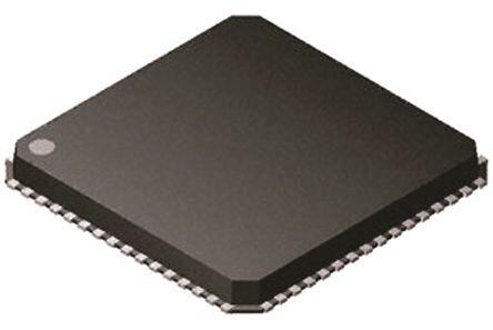
| 供应商器件封装 | 64-LFCSP-VQ(9x9) |
| 分辨率 | 16 bit |
| 包装 | 托盘 |
| 商标 | Analog Devices |
| 安装类型 | 表面贴装 |
| 安装风格 | SMD/SMT |
| 封装 | Tray |
| 封装/外壳 | 64-VFQFN 裸露焊盘,CSP |
| 封装/箱体 | CSP-64 |
| 工作温度 | -40°C ~ 105°C |
| 工厂包装数量 | 260 |
| 建立时间 | - |
| 接口类型 | SPI |
| 数据接口 | DSP,MICROWIRE™,QSPI™,串行,SPI™ |
| 最大功率耗散 | 173 mW |
| 最大工作温度 | + 105 C |
| 最小工作温度 | - 40 C |
| 标准包装 | 1 |
| 电压参考 | Internal, External |
| 电压源 | 模拟和数字,双 ± |
| 电源电压-最大 | 5.5 V |
| 电源电压-最小 | 2.7 V |
| 稳定时间 | 11 us |
| 系列 | AD5755 |
| 转换器数 | 4 |
| 转换器数量 | 4 |
| 输出数和类型 | 4 电流,4 电压 |
| 采样比 | 91 kSPs |
| 采样率(每秒) | - |


- 商务部:美国ITC正式对集成电路等产品启动337调查
- 曝三星4nm工艺存在良率问题 高通将骁龙8 Gen1或转产台积电
- 太阳诱电将投资9.5亿元在常州建新厂生产MLCC 预计2023年完工
- 英特尔发布欧洲新工厂建设计划 深化IDM 2.0 战略
- 台积电先进制程称霸业界 有大客户加持明年业绩稳了
- 达到5530亿美元!SIA预计今年全球半导体销售额将创下新高
- 英特尔拟将自动驾驶子公司Mobileye上市 估值或超500亿美元
- 三星加码芯片和SET,合并消费电子和移动部门,撤换高东真等 CEO
- 三星电子宣布重大人事变动 还合并消费电子和移动部门
- 海关总署:前11个月进口集成电路产品价值2.52万亿元 增长14.8%


PDF Datasheet 数据手册内容提取
Quad Channel, 16-Bit, Serial Input, 4 mA to 20 mA and Voltage Output DAC, Dynamic Power Control Data Sheet AD5755 FEATURES On-chip dynamic power control minimizes package power dissipation in current mode. This is achieved by regulating the 16-bit resolution and monotonicity voltage on the output driver from 7.4 V to 29.5 V using a dc-to- Dynamic power control for thermal management dc boost converter optimized for minimum on chip power Current and voltage output pins connectable to a single dissipation. terminal Current output ranges: 0 mA to 20 mA, 4 mA to 20 mA, The part uses a versatile 3-wire serial interface that operates at or 0 mA to 24 mA clock rates of up to 30 MHz and is compatible with standard ±0.05% total unadjusted error (TUE) maximum SPI, QSPI™, MICROWIRE™, DSP, and microcontroller inter- Voltage output ranges (with 20% overrange): 0 V to 5 V, 0 V face standards. The interface also features optional CRC-8 to 10 V, ±5 V, and ±10 V packet error checking, as well as a watchdog timer that ±0.04% total unadjusted error (TUE) maximum monitors activity on the interface. User programmable offset and gain PRODUCT HIGHLIGHTS On-chip diagnostics On-chip reference (±10 ppm/°C maximum) 1. Dynamic power control for thermal management. −40°C to +105°C temperature range 2. 16-bit performance. 3. Multichannel. APPLICATIONS COMPANION PRODUCTS Process control Actuator control Product Family: AD5755-1, AD5757 PLCs External References: ADR445, ADR02 Digital Isolators: ADuM1410, ADuM1411 GENERAL DESCRIPTION Power: ADP2302, ADP2303 The AD5755 is a quad, voltage and current output DAC that Additional companion products on the AD5755 product page operates with a power supply range from −26.4 V to +33 V. FUNCTIONAL BLOCK DIAGRAM AVCC 5.0V AVSS AVDD –15V AGND +15V SWx VBOOST_x DVDD 7.4V TO 29.5V DGND LDAC DC-TO-DC CONVERTER SCLK SDIN SYNC INDTIEGRITFAALCE IOUT_x SDO + DAC A RSET_x CLEAR CURRENT AND VOLTAGE FAULT OUTPUT RANGE ALERT GAIN REG A SCALING +VSENSE_x AD1 OFFSET REG A VOUT_x AD0 DAC CHANNEL A –VSENSE_x REFOUT REFERENCE REFIN DAC CHANNEL B DAC CHANNEL C AD5755 DAC CHANNEL D N1.O xT =E SA, B, C, AND D. 07304-100 Figure 1. Rev. E Document Feedback Information furnished by Analog Devices is believed to be accurate and reliable. However, no responsibility is assumed by Analog Devices for its use, nor for any infringements of patents or other One Technology Way, P.O. Box 9106, Norwood, MA 02062-9106, U.S.A. rights of third parties that may result from its use. Specifications subject to change without notice. No license is granted by implication or otherwise under any patent or patent rights of Analog Devices. Tel: 781.329.4700 ©2011–2017 Analog Devices, Inc. All rights reserved. Trademarks and registered trademarks are the property of their respective owners. Technical Support www.analog.com
AD5755 Data Sheet TABLE OF CONTENTS Features .............................................................................................. 1 Data Registers ............................................................................. 33 Applications ....................................................................................... 1 Control Registers ........................................................................ 35 General Description ......................................................................... 1 Readback Operation .................................................................. 38 Product Highlights ........................................................................... 1 Device Features ............................................................................... 40 Companion Products ....................................................................... 1 Output Fault ................................................................................ 40 Functional Block Diagram .............................................................. 1 Voltage Output Short-Circuit Protection ................................ 40 Revision History ............................................................................... 3 Digital Offset and Gain Control ............................................... 40 Detailed Functional Block Diagram .............................................. 4 Status Readback During a Write .............................................. 40 Specifications ..................................................................................... 5 Asynchronous Clear ................................................................... 41 AC Performance Characteristics ................................................ 8 Packet Error Checking ............................................................... 41 Timing Characteristics ................................................................ 9 Watchdog Timer ......................................................................... 41 Absolute Maximum Ratings .......................................................... 12 Output Alert ................................................................................ 41 ESD Caution ................................................................................ 12 Internal Reference ...................................................................... 42 Pin Configuration and Function Descriptions ........................... 13 External Current Setting Resistor ............................................ 42 Typical Performance Characteristics ........................................... 16 Digital Slew Rate Control .......................................................... 42 Voltage Outputs .......................................................................... 16 Power Dissipation Control ........................................................ 43 Current Outputs ......................................................................... 20 DC-to-DC Converters ............................................................... 43 DC-to-DC Block ......................................................................... 24 AI Supply Requirements—Static ............................................ 44 cc Reference ..................................................................................... 25 AI Supply Requirements—Slewing ...................................... 44 CC General ......................................................................................... 26 Applications Information .............................................................. 46 Terminology .................................................................................... 27 Voltage and Current Output Ranges on the Same Terminal 46 Theory of Operation ...................................................................... 29 Current Output Mode with Internal R ................................ 46 SET DAC Architecture ....................................................................... 29 Precision Voltage Reference Selection ..................................... 46 Power-On State of AD5755 ....................................................... 29 Driving Inductive Loads ............................................................ 47 Serial Interface ............................................................................ 30 Transient Voltage Protection .................................................... 47 Transfer Function ....................................................................... 30 Microprocessor Interfacing ....................................................... 47 Registers ........................................................................................... 31 Layout Guidelines....................................................................... 47 Programming Sequence to Write/Enable the Output Galvanically Isolated Interface ................................................. 48 Correctly ...................................................................................... 32 Outline Dimensions ....................................................................... 49 Changing and Reprogramming the Range ............................. 32 Ordering Guide .......................................................................... 49 Rev. E | Page 2 of 49
Data Sheet AD5755 REVISION HISTORY 6/2017—Rev. D to Rev. E 5/2012—Rev. A to Rev. B Changes to Figure 4......................................................................... 10 Changes to Figure 2 .......................................................................... 4 Changes to Figure 5......................................................................... 11 Changes to Figure 21 ...................................................................... 18 Changes to Readback Operation Section ..................................... 38 Changes to Figure 43 ...................................................................... 22 Deleted Table 28, Table 29, and Table 30; Renumbered Changes to Internal Reference Section ........................................ 41 Sequentially ...................................................................................... 38 Changes to Asynchronous Clear Section ..................................... 41 11/2011—Rev. 0 to Rev. A Updated Outline Dimensions ........................................................ 49 Changes to Figure 2 .......................................................................... 4 Changes to Ordering Guide ........................................................... 49 Changes to Table 1 ............................................................................ 5 Added Timing Diagram heading and changes to Figure 5........ 10 5/2014—Rev. C to Rev. D Changes to Figure 6 ........................................................................ 11 Changes to Thermal Hysteresis Parameter, Table 1 ...................... 7 Changes to Table 5 .......................................................................... 13 Changes to t Parameter, t Parameter, and t Parameter, Table 3 .... 9 Changes to Figure 13 ...................................................................... 16 6 9 19 Changes to Figure 4......................................................................... 10 Changes to Figure 21 ...................................................................... 18 Added Figure 5; Renumbered Sequentially, Change to Changes to Figure 37 ...................................................................... 20 Figure 6 ............................................................................................. 11 Changes to Figure 44 ...................................................................... 22 Changes to Figure 54, Figure 55, Figure 56, and Figure 57 ....... 24 Changes to Figure 56 and Figure 58 ............................................. 24 Change to Figure 65, Figure 68, and Figure 69 ........................... 26 Changes to Figure 71 ...................................................................... 29 Changes to Voltage Reference Thermal Hysteresis Section ...... 27 Changes to Power-On State of AD5575 Section ......................... 29 Changes to Table 12 and Table 14 ................................................. 34 Changes to Table 17 ........................................................................ 35 Changes to Readback Operation Section, Added Table 27, Changes to Readback Operation Section and changes to Table 28, and Table 29; Renumbered Sequentially ..................... 38 Table 26 ............................................................................................. 38 Changes to Status Readback During a Write Section ................. 41 Changes to Voltage Output Short-Circuit Protection Section .. 40 Changes to Packet Error Checking Section ................................. 42 Changes to Figure 78 ...................................................................... 41 Changes to Table 35 ........................................................................ 44 Changes to Figure 81 through Figure 84 Captions ..................... 44 Changes to Ordering Guide ........................................................... 50 Changes to Transient Voltage Protection Section and changes to Figure 85 ........................................................................................... 47 1/2013—Rev. B to Rev. C Changes to Galvanically Isolated Interface Section .................... 48 Changes to Figure 2........................................................................... 4 Changed Thermal Impedance from 20°C/W to 28°C/W .......... 12 5/2011—Revision 0: Initial Version Changes to Pin 6 Description, Table 5.......................................... 13 Changes to Figure 25 ...................................................................... 18 Changes to Bit DUT_AD1, DUT_AD0 Description, Table 9 ... 33 Changes to Packet Error Checking Section ................................. 41 Changes to Figure 79 ...................................................................... 43 Changes to Figure 84 ...................................................................... 47 Updated Outline Dimensions ........................................................ 49 Changes to Ordering Guide ........................................................... 49 Rev. E | Page 3 of 49
AD5755 Data Sheet DETAILED FUNCTIONAL BLOCK DIAGRAM AVCC 5.0V AVSS AVDD –15V AGND +15V SWA VBOOST_A DVDD POWER-ON DC-TO-DC DGND RESET CONVERTER LDAC POWER 7.4V TO 29.5V VSEN1 VSEN2 CONTROL REG CLEAR INPUT SHIFT SSCDLINK REGAINSDTER 16 INPUT + DAC 16 DAC A R2 R3 SYNC CONTROL REG A REG A SDO FAULT GAIN REG A IOUT_A OFFSET REG A STATUS REGISTER ALERT WATCHDOG R1 RSET_A TIMER (SPI ACTIVITY) 30kΩ +VSENSE_A REFOUT VREF VOUT RANGE VOUT_A SCALING REFIN REBFUEFRFEENRCSE DAC CHANNEL A –VSENSE_A IOUT_B, IOUT_C, IOUT_D DAC CHANNEL B RSET_B, RSET_C, RSET_D AD1 AD5755 DAC CHANNEL C AD0 DAC CHANNEL D +VSENSE_B, +VSENSE_C, +VSENSE_D SWB, SWC, SWD VBOOST_B,VBOOST_C,VBOOST_D VOUT_B,VOUT_C,VOUT_D 07304-001 Figure 2. Rev. E | Page 4 of 49
Data Sheet AD5755 SPECIFICATIONS AV = V = 15 V; AV = −15 V; DV = 2.7 V to 5.5 V; AV = 4.5 V to 5.5 V; dc-to-dc converter disabled; AGND = DGND = DD BOOST_x SS DD CC GNDSW = 0 V; REFIN = 5 V; voltage outputs: R = 1 kΩ, C = 220 pF; current outputs: R = 300 Ω; all specifications T to T , unless x L L L MIN MAX otherwise noted. Table 1. Parameter1 Min Typ Max Unit Test Conditions/Comments VOLTAGE OUTPUT Output Voltage Ranges 0 5 V 0 10 V −5 +5 V −10 +10 V 0 6 V 0 12 V −6 +6 V −12 +12 V Resolution 16 Bits ACCURACY AV = −15 V, loaded and unloaded SS Total Unadjusted Error (TUE) B Version −0.04 +0.04 % FSR −0.03 ±0.0032 +0.03 % FSR T = 25°C A A Version −0.25 +0.25 % FSR −0.075 ±0.02 +0.075 % FSR T = 25°C A TUE Long-Term Stability 35 ppm FSR Drift after 1000 hours, T = 150°C J Relative Accuracy (INL) −0.006 ±0.0012 +0.006 % FSR 0 V to 5 V, 0 V to 10 V, ±5 V, ±10 V ranges −0.008 ±0.0012 +0.008 % FSR On overranges Differential Nonlinearity (DNL) −1 +1 LSB Guaranteed monotonic Zero-Scale Error −0.03 ±0.002 +0.03 % FSR Zero-Scale TC2 ±2 ppm FSR/°C Bipolar Zero Error −0.03 ±0.002 +0.03 % FSR Bipolar Zero TC2 ±1 ppm FSR/°C Offset Error −0.03 ±0.002 +0.03 % FSR Offset TC2 ±2 ppm FSR/°C Gain Error −0.03 ±0.004 +0.03 % FSR Gain TC2 ±3 ppm FSR/°C Full-Scale Error −0.03 ±0.002 +0.03 % FSR Full-Scale TC2 ±2 ppm FSR/°C OUTPUT CHARACTERISTICS2 Headroom 1 2.2 V With respect to V supply BOOST Footroom 1 1.4 V With respect to the AV supply SS Output Voltage Drift vs. Time 20 ppm FSR Drift after 1000 hours, ¾ scale output, T = 150°C, J AV = −15 V SS Short-Circuit Current 12/6 16/8 mA Programmable by user, defaults to 16 mA typical level Load 1 kΩ For specified performance Capacitive Load Stability 10 nF 2 µF External compensation capacitor of 220 pF connected DC Output Impedance 0.06 Ω DC PSRR 50 µV/V DC Crosstalk 24 µV Rev. E | Page 5 of 49
AD5755 Data Sheet Parameter1 Min Typ Max Unit Test Conditions/Comments CURRENT OUTPUT Output Current Ranges 0 24 mA 0 20 mA 4 20 mA Resolution 16 Bits ACCURACY (EXTERNAL R ) Assumes ideal resistor; see the External Current SET Setting Resistor section for more information. Total Unadjusted Error (TUE) B Version −0.05 ±0.009 +0.05 % FSR A Version −0.2 ±0.04 +0.2 % FSR TUE Long-Term Stability 100 ppm FSR Drift after 1000 hours, T = 150°C J Relative Accuracy (INL) −0.006 +0.006 % FSR Differential Nonlinearity (DNL) −1 +1 LSB Guaranteed monotonic Offset Error −0.05 ±0.005 +0.05 % FSR Offset Error Drift2 ±4 ppm FSR/°C Gain Error −0.05 ±0.004 +0.05 % FSR Gain TC2 ±3 ppm FSR/°C Full-Scale Error −0.05 ±0.008 +0.05 % FSR Full-Scale TC2 ±5 ppm FSR/°C DC Crosstalk 0.0005 % FSR External R SET ACCURACY (INTERNAL R ) SET Total Unadjusted Error (TUE)3, 4 B Version −0.14 +0.14 % FSR −0.11 ±0.009 +0.11 % FSR T = 25°C A A Version −0.35 +0.35 % FSR −0.2 +0.04 +0.2 % FSR T = 25°C A TUE Long-Term Stability 180 ppm FSR Drift after 1000 hours, T = 150°C J Relative Accuracy (INL) −0.006 +0.006 % FSR Relative Accuracy (INL) −0.004 +0.004 % FSR T = 25°C A Differential Nonlinearity (DNL) −1 +1 LSB Guaranteed monotonic Offset Error3, 4 −0.05 +0.05 % FSR −0.04 ±0.007 +0.04 % FSR T = 25°C A Offset Error Drift2 ±6 ppm FSR/°C Gain Error −0.12 +0.12 % FSR −0.06 ±0.002 +0.06 % FSR T = 25°C A Gain TC2 ±9 ppm FSR/°C Full-Scale Error3, 4 −0.14 +0.14 % FSR −0.1 ±0.007 +0.1 % FSR T = 25°C A Full-Scale TC2 ±14 ppm FSR/°C DC Crosstalk4 −0.011 % FSR Internal R SET OUTPUT CHARACTERISTICS2 Current Loop Compliance Voltage V V − V BOOST_x BOOST_x − 2.4 2.7 Output Current Drift vs. Time Drift after 1000 hours, ¾ scale output, T = 150°C J 90 ppm FSR External R SET 140 ppm FSR Internal R SET Rev. E | Page 6 of 49
Data Sheet AD5755 Parameter1 Min Typ Max Unit Test Conditions/Comments Resistive Load 1000 Ω The dc-to-dc converter has been characterized with a maximum load of 1 kΩ, chosen such that compliance is not exceeded; see Figure 53 and DC-DC MaxV bits in Table 25 Output Impedance 100 MΩ DC PSRR 0.02 1 µA/V REFERENCE INPUT/OUTPUT Reference Input2 Reference Input Voltage 4.95 5 5.05 V For specified performance DC Input Impedance 45 150 MΩ Reference Output Output Voltage 4.995 5 5.005 V T = 25°C A Reference TC2 −10 ±5 +10 ppm/°C Output Noise (0.1 Hz to 10 Hz)2 7 µV p-p Noise Spectral Density2 100 nV/√Hz At 10 kHz Output Voltage Drift vs. Time2 180 ppm Drift after 1000 hours, T = 150°C J Capacitive Load2 1000 nF Load Current 9 mA See Figure 64 Short-Circuit Current 10 mA Line Regulation2 3 ppm/V See Figure 65 Load Regulation2 95 ppm/mA See Figure 64 Thermal Hysteresis2 200 ppm DC-TO-DC Switch Switch On Resistance 0.425 Ω Switch Leakage Current 10 nA Peak Current Limit 0.8 A Oscillator Oscillator Frequency 11.5 13 14.5 MHz This oscillator is divided down to give the dc-to-dc converter switching frequency Maximum Duty Cycle 89.6 % At 410 kHz dc-to-dc switching frequency DIGITAL INPUTS2 JEDEC compliant V , Input High Voltage 2 V IH V , Input Low Voltage 0.8 V IL Input Current −1 +1 µA Per pin Pin Capacitance 2.6 pF Per pin DIGITAL OUTPUTS2 SDO, ALERT V , Output Low Voltage 0.4 V Sinking 200 µA OL V , Output High Voltage DVDD − V Sourcing 200 µA OH 0.5 High Impedance Leakage −1 +1 µA Current High Impedance Output 2.5 pF Capacitance FAULT V , Output Low Voltage 0.4 V 10 kΩ pull-up resistor to DV OL DD V , Output Low Voltage 0.6 V At 2.5 mA OL V , Output High Voltage 3.6 V 10 kΩ pull-up resistor to DV OH DD POWER REQUIREMENTS AV 9 33 V DD AV −26.4 −10.8 V SS DV 2.7 5.5 V DD AV 4.5 5.5 V CC Rev. E | Page 7 of 49
AD5755 Data Sheet Parameter1 Min Typ Max Unit Test Conditions/Comments AI 8.6 10.5 mA Voltage output mode on all channels, output DD unloaded, over supplies 7 7.5 mA Current output mode on all channels, AI −11 −8.8 mA Voltage output mode on all channels, output SS unloaded, over supplies −1.7 mA Current output mode on all channels DI 9.2 11 mA V = DV , V = DGND, internal oscillator running, CC IH DD IL over supplies AI 1 mA Output unloaded, over supplies CC I 5 2.7 mA Per channel, voltage output mode, output BOOST unloaded, over supplies 1 mA Per channel, current output mode Power Dissipation 173 mW AV = 15 V, AV = −15 V, dc-to-dc converter DD SS enable, current output mode, outputs disabled 1 Temperature range: −40°C to +105°C; typical at +25°C. 2 Guaranteed by design and characterization; not production tested. 3 For current outputs with internal RSET, the offset, full-scale, and TUE measurements exclude dc crosstalk. The measurements are made with all four channels enabled loaded with the same code. 4 See the Current Output Mode with Internal RSET section for more explanation of the dc crosstalk. 5 Efficiency plots in Figure 55, Figure 56, Figure 57, and Figure 58 include the IBOOST quiescent current. AC PERFORMANCE CHARACTERISTICS AV = V = 15 V; AV = −15 V; DV = 2.7 V to 5.5 V; AV = 4.5 V to 5.5 V; dc-to-dc converter disabled; AGND = DGND = DD BOOST_x SS DD CC GNDSW = 0 V; REFIN = 5 V; voltage outputs: R = 2 kΩ, C = 220 pF; current outputs: R = 300 Ω; all specifications T to T , unless x L L L MIN MAX otherwise noted. Table 2. Parameter1 Min Typ Max Unit Test Conditions/Comments DYNAMIC PERFORMANCE Voltage Output Output Voltage Settling Time 11 µs 5 V step to ±0.03% FSR, 0 V to 5 V range 18 µs 10 V step to ±0.03% FSR, 0 V to 10 V range 13 µs 100 mV step to 1 LSB (16-bit LSB), 0 V to 10 V range Slew Rate 1.9 V/µs 0 V to 10 V range Power-On Glitch Energy 150 nV-sec Digital-to-Analog Glitch Energy 6 nV-sec Glitch Impulse Peak Amplitude 25 mV Digital Feedthrough 1 nV-sec DAC to DAC Crosstalk 2 nV-sec 0 V to 10 V range Output Noise (0.1 Hz to 10 Hz 0.15 LSB p-p 16-bit LSB, 0 V to 10 V range Bandwidth) Output Noise Spectral Density 150 nV/√Hz Measured at 10 kHz, midscale output, 0 V to 10 V range AC PSRR 83 dB 200 mV 50 Hz/60 Hz sine wave superimposed on power supply voltage Current Output Output Current Settling Time 15 µs To 0.1% FSR (0 mA to 24 mA) See test conditions/ ms See Figure 49, Figure 50, and Figure 51 comments Output Noise (0.1 Hz to 10 Hz 0.15 LSB p-p 16-bit LSB, 0 mA to 24 mA range Bandwidth) Output Noise Spectral Density 0.5 nA/√Hz Measured at 10 kHz, midscale output, 0 mA to 24 mA range 1 Guaranteed by design and characterization; not production tested. Rev. E | Page 8 of 49
Data Sheet AD5755 TIMING CHARACTERISTICS AV = V = 15 V; AV = −15 V; DV = 2.7 V to 5.5 V; AV = 4.5 V to 5.5 V; dc-to-dc converter disabled; AGND = DGND = DD BOOST_x SS DD CC GNDSW = 0 V; REFIN = 5 V; voltage outputs: R = 1 kΩ, C = 220 pF; current outputs: R = 300 Ω; all specifications T to T , unless x L L L MIN MAX otherwise noted. Table 3. Parameter1, 2, 3 Limit at T , T Unit Description MIN MAX t 33 ns min SCLK cycle time 1 t 13 ns min SCLK high time 2 t 13 ns min SCLK low time 3 t4 13 ns min SYNC falling edge to SCLK falling edge setup time t5 13 ns min 24th/32nd SCLK falling edge to SYNC rising edge (see Figure 78) t6 198 ns min SYNC high time after a configuration write 5 µs min SYNC high time after a DAC update write t 5 ns min Data setup time 7 t 5 ns min Data hold time 8 t9 20 µs min SYNC rising edge to LDAC falling edge (applies to any channel with digital slew rate control enabled; single DAC updated) 5 µs min SYNC rising edge to LDAC falling edge (single DAC updated) t10 10 ns min LDAC pulse width low t11 500 ns max LDAC falling edge to DAC output response time t See the AC Performance µs max DAC output settling time 12 Characteristics section t 10 ns min CLEAR high time 13 t 5 µs max CLEAR activation time 14 t 40 ns max SCLK rising edge to SDO valid 15 t16 5 µs min SYNC rising edge to DAC output response time (LDAC = 0) (single DAC updated) t17 500 ns min LDAC falling edge to SYNC rising edge t18 800 ns min RESET pulse width t19 20 µs min SYNC high to next SYNC low (digital slew rate control enabled) (single DAC updated) 5 µs min SYNC high to next SYNC low (digital slew rate control disabled) (single DAC updated) 1 Guaranteed by design and characterization; not production tested. 2 All input signals are specified with tRISE = tFALL = 5 ns (10% to 90% of DVDD) and timed from a voltage level of 1.2 V. 3 See Figure 3, Figure 4, Figure 6, and Figure 7. Rev. E | Page 9 of 49
AD5755 Data Sheet Timing Diagrams t1 SCLK 1 2 24 t6 t3 t2 t4 t5 SYNC t7 t8 t19 SDIN MSB LSB t10 t10 t9 LDAC t17 t12 t11 VOUT_x LDAC = 0 t12 t16 VOUT_x t13 CLEAR t14 VOUT_x RESET t18 07304-002 Figure 3. Serial Interface Timing Diagram SCLK 1 24 1 24 t6 SYNC SDIN MSB LSB MSB LSB INPUTWORDSPECIFIES NOPCONDITION REGISTERTOBEREAD SDO MSB LSB UNDEFINED t15 SELECCTLEODCRKEEGDISOTUETRDATA 07304-304 Figure 4. Readback Timing Diagram (Packet Error Checking Disabled) Rev. E | Page 10 of 49
Data Sheet AD5755 SCLK 1 24 32 1 24 32 t61 SYNC SDIN MSB LSB CRC7 CRC0 MSB LSB CRC7 CRC0 INPUTWORDSPECIFIES 8-BITCRC NOP 8-BITCRC REGISTERTOBEREAD CONDITION SDO MSB LSB UNDEFINED 8-BITCRC t15 SELECTED REGISTER DATA CLOCKED OUT 1 SAEVEO TIDH ES CRLEKA ADCBTAICVKIT OY P DEURRAITNIGONt6 AANSD I TP AMCAKYE RTE ESRURLOT RIN C AH EPCEKCI NEGRR SOERC TOION NRSE AFODBRA FCUKR.THER INFORMATION. 07304-305 Figure 5. Readback Timing Diagram (Packet Error Checking Enabled) LSB MSB 1 2 24 SCLK SYNC SDIN R/W DUT_ DUT_ X X X D15 D14 D1 D0 AD1 AD0 SDO SDO DISABLED ESNDAOB_ STATUS STATUS STATUS STATUS 07304-104 Figure 6. Status Readback During Write 200µA IOL TO OUTPUT VOH (MIN) OR PIN CL VOL (MAX) 50pF 200µA IOH 07304-005 Figure 7. Load Circuit for SDO Timing Diagram Rev. E | Page 11 of 49
AD5755 Data Sheet ABSOLUTE MAXIMUM RATINGS T = 25°C, unless otherwise noted. Transient currents of up to Stresses at or above those listed under Absolute Maximum A 100 mA do not cause SCR latch-up. Ratings may cause permanent damage to the product. This is a stress rating only; functional operation of the product at these Table 4. or any other conditions above those indicated in the operational Parameter Rating section of this specification is not implied. Operation beyond AV , V to AGND, DGND −0.3 V to +33 V DD BOOST_x the maximum operating conditions for extended periods may AV to AGND, DGND +0.3 V to −28 V SS affect product reliability. AV to AV −0.3 V to +60 V DD SS AV to AGND −0.3 V to +7 V CC DV to DGND −0.3 V to +7 V ESD CAUTION DD Digital Inputs to DGND −0.3 V to DV + 0.3 V or +7 V DD (whichever is less) Digital Outputs to DGND −0.3 V to DV + 0.3 V or +7 V DD (whichever is less) REFIN, REFOUT to AGND −0.3 V to AV + 0.3 V or +7 V DD (whichever is less) V to AGND AV to V or 33 V if using OUT_x SS BOOST_x the dc-to-dc circuitry +V , −V to AGND AV to V or 33 V if using SENSE_x SENSE_x SS BOOST_x the dc-to-dc circuitry I to AGND AV to V or 33 V if using OUT_x SS BOOST_x the dc-to-dc circuitry SW to AGND −0.3 to +33 V x AGND, GNDSW to DGND −0.3 V to +0.3 V x Operating Temperature Range (T) A Industrial1 −40°C to +105°C Storage Temperature Range −65°C to +150°C Junction Temperature (T max) 125°C J 64-Lead LFCSP θ Thermal Impedance2 28°C/W JA Power Dissipation (T max − T )/θ J A JA Lead Temperature JEDEC industry standard Soldering J-STD-020 1 Power dissipated on chip must be derated to keep the junction temperature below 125°C. 2 Based on a JEDEC 4-layer test board. Rev. E | Page 12 of 49
Data Sheet AD5755 PIN CONFIGURATION AND FUNCTION DESCRIPTIONS D RSET_CRSET_DREFOUTREFINCOMPLV_D–VSENSE_D+VSENSE_DCOMPDCDC_VBOOST_DVOUT_DIOUT_DAVSSCOMPLV_C–VSENSE_C+VSENSE_CVOUT_C 4321098765432109 6666655555555554 PIN 1 INDICATOR RSET_B 1 48COMPDCDC_C RSET_A 2 47IOUT_C REFGND 3 46VBOOST_C REFGND 4 45AVCC AD0 5 44SWC AD1 6 43GNDSWC SYNC 7 AD5755 42GNDSWD SCLK 8 TOP VIEW 41SWD SDIN 9 (Not to Scale) 40AVSS SDO10 39SWA DVDD11 38GNDSWA DGND12 37GNDSWB LDAC13 36SWB CLEAR14 35AGND ALERT15 34VBOOST_B FAULT16 33IOUT_B 7890123456789012 1112222222222333 POCRESETAVDDCOMPLV_A–VSENSE_A+VSENSE_AOMPDCDC_AVBOOST_AVOUT_AIOUT_AAVSSCOMPLV_B–VSENSE_B+VSENSE_BVOUT_BOMPDCDC_B C C NOTES 1.THIS EXPOSED PADDLE SHOULD BE CONNECTED TO THE POTENTIALOF THE ICATOV ISPSSP R PEEIRNC ,PO OLMARMN, EAENL FDTOEERDR NETANHTHAIATVN ETCLHYEE,D PI TTA HCDEADRNLM EBA EBL EL P ETEFHRTEF REOMLREAMCLATLNRYCI CCEAO.LNLNYE UCNTECDO NTNOE ACTED. 07304-006 Figure 8. Pin Configuration Table 5. Pin Function Descriptions Pin No. Mnemonic Description 1 R An external, precision, low drift 15 kΩ current setting resistor can be connected to this pin to improve the I SET_B OUT_B temperature drift performance. See the Device Features section. 2 R An external, precision, low drift 15 kΩ current setting resistor can be connected to this pin to improve the I SET_A OUT_A temperature drift performance. See the Device Features section. 3 REFGND Ground Reference Point for Internal Reference. 4 REFGND Ground Reference Point for Internal Reference. 5 AD0 Address Decode for the Device Under Test (DUT) on the Board. 6 AD1 Address Decode for the DUT on the Board. It is not recommended to tie both AD1 and AD0 low when using PEC, see the Packet Error Checking section. 7 SYNC Active Low Input. This is the frame synchronization signal for the serial interface. While SYNC is low, data is transferred in on the falling edge of SCLK. 8 SCLK Serial Clock Input. Data is clocked into the input shift register on the falling edge of SCLK. This operates at clock speeds of up to 30 MHz. 9 SDIN Serial Data Input. Data must be valid on the falling edge of SCLK. 10 SDO Serial Data Output. Used to clock data from the serial register in readback mode. See Figure 4 and Figure 6. 11 DV Digital Supply. The voltage range is from 2.7 V to 5.5 V. DD 12 DGND Digital Ground. 13 LDAC Load DAC, Active Low Input. This is used to update the DAC register and consequently the DAC outputs. When tied permanently low, the addressed DAC data register is updated on the rising edge of SYNC. If LDAC is held high during the write cycle, the DAC input register is updated, but the DAC output update only takes place at the falling edge of LDAC (see Figure 3). Using this mode, all analog outputs can be updated simultaneously. The LDAC pin must not be left unconnected. 14 CLEAR Active High, Edge Sensitive Input. Asserting this pin sets the output current and voltage to the preprogrammed clear code bit setting. Only channels enabled to be cleared are cleared. See the Device Features section for more information. When CLEAR is active, the DAC output register cannot be written to. Rev. E | Page 13 of 49
AD5755 Data Sheet Pin No. Mnemonic Description 15 ALERT Active High Output. This pin is asserted when there has been no SPI activity on the interface pins for a predetermined time. See the Device Features section for more information. 16 FAULT Active Low Output. This pin is asserted low when an open circuit in current mode is detected, a short circuit in voltage mode is detected, a PEC error is detected, or an overtemperature is detected (see the Device Features section). Open-drain output. 17 POC Power-On Condition. This pin determines the power-on condition and is read during power-on or, alternatively, after a device reset. If POC = 0, the device is powered up with the voltage and current channels in tristate mode. If POC = 1, the device is powered up with a 30 kΩ pull-down resistor to ground on the voltage output channel, and the current channel is in tristate mode. 18 RESET Hardware Reset, Active Low Input. 19 AV Positive Analog Supply. The voltage range is from 9 V to 33 V. DD 20 COMP Optional Compensation Capacitor Connection for V Output Buffer. Connecting a 220 pF capacitor between LV_A OUT_A this pin and the V pin allows the voltage output to drive up to 2 µF. Note that the addition of this capacitor OUT_A reduces the bandwidth of the output amplifier, increasing the settling time. 21 −V Sense Connection for the Negative Voltage Output Load Connection for V . This pin must stay within ±3.0 V SENSE_A OUT_A of AGND for specified operation. 22 +V Sense Connection for the Positive Voltage Output Load Connection for V . SENSE_A OUT_A 23 COMP DC-to-DC Compensation Capacitor. Connect a 10 nF capacitor from this pin to ground. Used to regulate the DCDC_A feedback loop of the Channel A dc-to-dc converter. Alternatively, if using an external compensation resistor, place a resistor in series with a capacitor to ground from this pin (see the DC-to-DC Converter Compensation Capacitors and the AI Supply Requirements—Slewing sections in the Device Features section for more CC information). 24 V Supply for Channel A Current Output Stage (see Figure 73). This is also the supply for the V stage, which is BOOST_A OUT_x regulated to 15 V by the dc-to-dc converter. To use the dc-to-dc feature of the device, connect as shown in Figure 79. 25 V Buffered Analog Output Voltage for DAC Channel A. OUT_A 26 I Current Output Pin for DAC Channel A. OUT_A 27 AV Negative Analog Supply Pin. Voltage range is from −10.8 V to −26.4 V. SS 28 COMP Optional Compensation Capacitor Connection for V Output Buffer. Connecting a 220 pF capacitor between LV_B OUT_B this pin and the V pin allows the voltage output to drive up to 2 µF. Note that the addition of this capacitor OUT_B reduces the bandwidth of the output amplifier, increasing the settling time. 29 −V Sense Connection for the Negative Voltage Output Load Connection for V . This pin must stay within ±3.0 V SENSE_B OUT_B of AGND for specified operation. 30 +V Sense Connection for the Positive Voltage Output Load Connection for V . SENSE_B OUT_B 31 V Buffered Analog Output Voltage for DAC Channel B. OUT_B 32 COMP DC-to-DC Compensation Capacitor. Connect a 10 nF capacitor from this pin to ground. Used to regulate the DCDC_B feedback loop of the Channel B dc-to-dc converter. Alternatively, if using an external compensation resistor, place a resistor in series with a capacitor to ground from this pin (see the DC-to-DC Converter Compensation Capacitors and the AI Supply Requirements—Slewing sections in the Device Features section for more CC information). 33 I Current Output Pin for DAC Channel B. OUT_B 34 V Supply for Channel B Current Output Stage (see Figure 73). This is also the supply for the V stage, which is BOOST_B OUT_x regulated to 15 V by the dc-to-dc converter. To use the dc-to-dc feature of the device, connect as shown in Figure 79. 35 AGND Ground Reference Point for Analog Circuitry. This must be connected to 0 V. 36 SW Switching Output for Channel B DC-to-DC Circuitry. To use the dc-to-dc feature of the device, connect as shown B in Figure 79. 37 GNDSW Ground Connection for DC-to-DC Switching Circuit. This pin should always be connected to ground. B 38 GNDSW Ground Connection for DC-to-DC Switching Circuit. This pin should always be connected to ground. A 39 SW Switching Output for Channel A DC-to-DC Circuitry. To use the dc-to-dc feature of the device, connect as shown A in Figure 79. 40 AV Negative Analog Supply Pin. The voltage range is from −10.8 V to −26.4 V. SS 41 SW Switching Output for Channel D DC-to-DC Circuitry. To use the dc-to-dc feature of the device, connect as shown D in Figure 79. 42 GNDSW Ground Connections for DC-to-DC Switching Circuit. This pin should always be connected to ground. D 43 GNDSW Ground Connections for DC-to-DC Switching Circuit. This pin should always be connected to ground. C Rev. E | Page 14 of 49
Data Sheet AD5755 Pin No. Mnemonic Description 44 SW Switching Output for Channel C DC-to-DC Circuitry. To use the dc-to-dc feature of the device, connect as shown C in Figure 79. 45 AV Supply for DC-to-DC Circuitry. CC 46 V Supply for Channel C Current Output Stage (see Figure 73). This is also the supply for the V stage, which is BOOST_C OUT_x regulated to 15 V by the dc-to-dc converter. To use the dc-to-dc feature of the device, connect as shown in Figure 79. 47 I Current Output Pin for DAC Channel C. OUT_C 48 COMP DC-to-DC Compensation Capacitor. Connect a 10 nF capacitor from this pin to ground. Used to regulate the DCDC_C feedback loop of the Channel C dc-to-dc converter. Alternatively, if using an external compensation resistor, place a resistor in series with a capacitor to ground from this pin (see the DC-to-DC Converter Compensation Capacitors and AI Supply Requirements—Slewing sections in the Device Features section for more CC information). 49 V Buffered Analog Output Voltage for DAC Channel C. OUT_C 50 +V Sense Connection for the Positive Voltage Output Load Connection for V . SENSE_C OUT_C 51 −V Sense Connection for the Negative Voltage Output Load Connection for V . This pin must stay within ±3.0 V SENSE_C OUT_C of AGND for specified operation. 52 COMP Optional Compensation Capacitor Connection for V Output Buffer. Connecting a 220 pF capacitor between LV_C OUT_C this pin and the V pin allows the voltage output to drive up to 2 µF. Note that the addition of this capacitor OUT_C reduces the bandwidth of the output amplifier, increasing the settling time. 53 AV Negative Analog Supply Pin. SS 54 I Current Output Pin for DAC Channel D. OUT_D 55 V Buffered Analog Output Voltage for DAC Channel D. OUT_D 56 V Supply for Channel D Current Output Stage (see Figure 73). This is also the supply for the V stage, which is BOOST_D OUT_x regulated to 15 V by the dc-to-dc converter. To use the dc-to-dc feature of the device, connect as shown in Figure 79. 57 COMP DC-to-DC Compensation Capacitor. Connect a 10 nF capacitor from this pin to ground. Used to regulate the DCDC_D feedback loop of Channel D dc-to-dc converter. Alternatively, if using an external compensation resistor, place a resistor in series with a capacitor to ground from this pin (see the DC-to-DC Converter Compensation Capacitors and AI Supply Requirements—Slewing sections in the Device Features section for more information). CC 58 +V Sense Connection for the Positive Voltage Output Load Connection for V . SENSE_D OUT_D 59 −V Sense Connection for the Negative Voltage Output Load Connection for V . This pin must stay within ±3.0 V SENSE_D OUT_D of AGND for specified operation. 60 COMP Optional Compensation Capacitor Connection for V Output Buffer. Connecting a 220 pF capacitor between LV_D OUT_D this pin and the V pin allows the voltage output to drive up to 2 µF. Note that the addition of this capacitor OUT_D reduces the bandwidth of the output amplifier, increasing the settling time. 61 REFIN External Reference Voltage Input. 62 REFOUT Internal Reference Voltage Output. It is recommended to place a 0.1 µF capacitor between REFOUT and REFGND. 63 R An external, precision, low drift 15 kΩ current setting resistor can be connected to this pin to improve the I SET_D OUT_D temperature drift performance. See the Device Features section. 64 R An external, precision, low drift 15 kΩ current setting resistor can be connected to this pin to improve the I SET_C OUT_C temperature drift performance. See the Device Features section. EPAD Exposed Pad. This exposed pad should be connected to the potential of the AV pin, or, alternatively, it can be SS left electrically unconnected. It is recommended that the pad be thermally connected to a copper plane for enhanced thermal performance. Rev. E | Page 15 of 49
AD5755 Data Sheet TYPICAL PERFORMANCE CHARACTERISTICS VOLTAGE OUTPUTS 0.0015 0.0015 ±10V RANGE AVDD = +15V ±5V RANGE AVSS = –15V 0.0010 ++150VV R RAANNGGEE TA = 25°C 0.0010 +10V RANGE WITH DCDC R) 0.0005 +5V RANGE MAX INL +10V RANGE MAX INL S ROR (%F 0.0005 L (%FSR) 0 ±+±555VVV RRRAAANNNGGGEEE MMMAIINNX II NNINLLL ±+±111000VVV RRRAAANNNGGGEEE MMMAIINNX II NNINLLL ER 0 IN AVDD = +15V INL –0.0005 AOVUSTSP U= T– 1U5NVLOADED –0.0005 –0.0010 –0.00100 10k 20k 3C0kODE 40k 50k 60k 07304-023 –0.0015–40 –20 0 TEM2P0ERATU4R0E (°C)60 80 100 07304-127 Figure 9. Integral Nonlinearity Error vs. DAC Code Figure 12. Integral Nonlinearity Error vs. Temperature 1.0 1.0 00..68 ±±++15150V0VVV RR RRAAAANNNNGGGGEEEE ATAAVV DS=SD 2 ==5 °–+C1155VV 00..68 AAAVLVLDSS DR ==A N–+11G55EVVS +10V RANGE WITH DCDC 0.4 0.4 B) B) S S L 0.2 L 0.2 R ( R ( RRO 0 RRO 0 DDNNLL EERRRROORR MMAINX E E L –0.2 L –0.2 N N D D –0.4 –0.4 –0.6 –0.6 –0.8 –0.8 –1.00 10k 20k 30kCODE 40k 50k 60k 07304-024 –1.0–40 –20 0 TEM2P0ERATU4R0E (°C)60 80 100 07304-128 Figure 10. Differential Nonlinearity Error vs. DAC Code Figure 13. Differential Nonlinearity Error vs. Temperature 0.006 0.012 %FSR) 00..000024 ±±+++151510V0V0VVV RR RRRAAAAANNNNNGGGGGEEEEE WITH DATACAVVD DS=CSD 2 ==5 °–+C1155VV %FSR) 00..000180 ++±±5151V0V0VV RR RRAAAANNNNGGGGEEEE R ( R ( AVDD = +15V RRO 0 RRO 0.006 AOVUSTSP U= T– 1U5NVLOADED E E D D 0.004 TE–0.002 TE US US 0.002 DJ–0.004 DJ NA NA 0 U U L –0.006 L A A–0.002 T T O O T–0.008 T–0.004 –0.0100 10k 20k 30kCODE 40k 50k 60k 07304-025 –0.006–40 –20 0 TEM2P0ERATU4R0E (°C)60 80 100 07304-129 Figure 11. Total Unadjusted Error vs. DAC Code Figure 14. Total Unadjusted Error vs. Temperature Rev. E | Page 16 of 49
Data Sheet AD5755 0.012 0.010 +5V RANGE 0.010 +±51V0V R RAANNGGEE 0.008 ++51V0V R RAANNGGEE ±10V RANGE ±5V RANGE OR (%FSR) 00..000068 AOAVVUDSTSDP U== T–+ 11U55NVVLOADED %FSR) 00..000046 AOAVVU±DST1SDP0 U==V T –+R 11UA55NVNVLGOEADED CALE ERR 00..000024 N ERROR ( 0.0020 L-S 0 GAI L U –0.002 F–0.002 –0.004 –0.004 –0.006–40 –20 0 TEM2P0ERATU4R0E (°C)60 80 100 07304-132 –0.006–40 –20 0 TEM2P0ERATU4R0E (°C)60 80 100 07304-135 Figure 15. Full-Scale Error vs. Temperature Figure 18. Gain Error vs. Temperature 0.0015 0.0015 0.0010 0.0010 R) 0.0005 S F 0.0005 % ET (%FSR)–0.00050 E ERROR ( 0 FS AL–0.0005 OF––00..00001150 AVD++D51 V0=V +R R1A5ANVNGGEE ERO-SC–0.0010 ++±551VV0V RR RAAANNNGGGEEE AVSS = –15V Z ±10V RANGE OUTPUT UNLOADED –0.0015 AVDD = +15V –0.0020 AVSS = –15V OUTPUT UNLOADED –0.002–540 –20 0 TEM2P0ERATU4R0E (°C)60 80 100 07304-133 –0.0020–40 –20 0 TEM2P0ERATU4R0E (°C)60 80 100 07304-136 Figure 16. Offset Error vs. Temperature Figure 19. Zero-Scale Error vs. Temperature 0.0025 0.0020 0.0020 0.0015 FSR) 0.0015 0.0010 % R ( 0.0010 R) O S 0.0005 RR 0.0005 %F 0V TO 10V RANGE MAX INL LAR ZERO E–0.00050 ±±15V0V R RAANNGGEE INL EROR (–0.00050 A0TVAV ST=S O2 = 51 °–0C2V6 R.4AVN FGOER M AIVND IDN L> +26.4V BIPO–0.0010 AAVVDSSD == –+1155VV –0.0010 OUTPUT UNLOADED –0.0015 –0.0015 –0.002–040 –20 0 TEM2P0ERATU4R0E (°C)60 80 100 07304-134 –0.002010 15 S2U0PPLY (V) 25 30 07304-034 Figure 17. Bipolar Zero Error vs. Temperature Figure 20. Integral Nonlinearity Error vs. AVDD/|AVSS| Rev. E | Page 17 of 49
AD5755 Data Sheet 1.0 12 0.8 AAAVLVLDSS DR ==A N–+11G55EVVS 8 A±A1VV0DSVSD R ==A –+N11G55VVE 0.6 TA = 25°C TA = 25°C 0.4 AVSS = –26.4V FOR AVDD > +26.4V V) OUTPUT UNLOADED ERROR (LSB) 0.20 DDNNLL EERRRROORR MMAINX T VOLTAGE ( 40 DNL –0.2 UTPU –4 –0.4 O –0.6 –8 –0.8 –1.010 15 S2U0PPLY (V) 25 30 07304-138 –12–5 0 TIME5 (µs) 10 15 07304-037 Figure 21. Differential Nonlinearity Error vs. AVDD/|AVSS| Figure 24. Full-Scale Positive Step 0.008 12 0V TO 10V RANGE MAX TUE AVDD = +15V SR) 0.006 0TVA =T O25 1°0CV RANGE MIN TUE 8 A±1V0SVS R=A –N1G5VE %F AVSS = –26.4V FOR AVDD > +26.4V TA = 25°C R ( V) OUTPUT UNLOADED RO 0.004 E ( 4 R G E A USTED 0.002 T VOLT 0 J U D P NA 0 UT –4 U O L A T O –0.002 –8 T –0.00410 15 S2U0PPLY (V) 25 30 07304-035 –12–5 0 TIME5 (µs) 10 15 07304-038 Figure 22. Total Unadjusted Error vs. AVDD/|AVSS| Figure 25. Full-Scale Negative Step 0.0020 15 8mA LIMIT, CODE = 0xFFFF 0x7FFF TO 0x8000 0.0015 16mA LIMIT, CODE = 0xFFFF 10 0x8000 TO 0x7FFF AVDD = +15V E DELTA (V) 00..00001005 AGE (mV) 50 A±T1AV0 S=VS 2 R=5A º–CN1G5VE G T TA 0 OL L V T VO–0.0005 PUT –5 U T TP OU –10 OU–0.0010 AVDD = +15V AVSS = –15V –0.0015 ±10V RANGE –15 TA = 25°C EXTERNAL RESISTOR = VISHAY S102C, 0.6ppm –0.0020–20 –16 –12 –8OUTP–U4T CU0RREN4T (mA)8 12 16 20 07304-036 –200 1 2 TIME (µs)3 4 5 07304-039 Figure 23. Source and Sink Capability of Output Amplifier Figure 26. Digital-to-Analog Glitch Rev. E | Page 18 of 49
Data Sheet AD5755 15 60 AVDD = +15V AVSS = –15V 40 ±10V RANGE 10 TA = 25°C 20 OUTPUT UNLOADED E (µV) 5 E (mV) 0 G G –20 A A OLT 0 OLT –40 V V UT UT –60 POC = 1 P P OUT –5 OUT –80 AVDDP O= C+ 1=5 V0 –100 AVSS = –15V –10 ±10V RANGE –120 TA = 25°C INT_ENABLE = 1 –150 1 2 3 4 TIM5E (s) 6 7 8 9 10 07304-040 –1400 2 4TIME (µs)6 8 10 07304-044 Figure 27. Peak-to-Peak Noise (0.1 Hz to 10 Hz Bandwidth) Figure 30. VOUT_x vs. Time on Output Enable 300 0 AVDD = +15V ±10V RANGE OUTPUT UNLOADED AVSS = –15V TA = 25°C AVDD = +15V VBOOST = +15V 200 –20 AVSS = –15V TA = 25°C V) E (µ 100 dB) –40 AG R ( T R OL 0 PS –60 V X UT UT_ P O T –100 V –80 U O –200 –100 –3000 1 2 3 4 TIME5 (µs)6 7 8 9 10 07304-041 –12010 100 1kFREQU1E0NkCY (Hz)100k 1M 10M 07304-045 Figure 28. Peak-to-Peak Noise (100 kHz Bandwidth) Figure 31. VOUT_x PSRR vs. Frequency 25 20 15 mV) 10 E ( G 5 A T OL 0 V UT –5 P T U –10 O –15 AVDD = +15V –20 AVSS = –15V TA = 25°C –250 25 50TIME (µs)75 100 125 07304-043 Figure 29. VOUT_x vs. Time on Power-Up Rev. E | Page 19 of 49
AD5755 Data Sheet CURRENT OUTPUTS 0.0025 0.0010 AAVVDSSD == –+1155VV SR) 0.0008 TA = 25°C %F 0.0015 R ( 0.0006 O INL ERROR (%FSR)–00..00000055 L NONLINEARITY ERR––0000....00000000000042240 400400mmmmmmAAAAAA TTTTTTOOOOOO 222222004040mmmmmmAAAAAA RRRRRRAAAAAANNNNNNGGGGGGEEEEEE MMMMMMAAAAIINNXXXX II NNIIIINNNNLLLLLL AAVVDSSD == –+1155VV A –0.0015 4mATO 20mA, EXTERNAL RSET GR–0.0006 4mATO 20mA, EXTERNAL RSET, WITH DC-TO-DC CONVERTER TE 44mmAATTOO 2200mmAA,, IINNTTEERRNNAALL RRSSEETT, WITH DC-TO-DC CONVERTER IN–0.0008 –0.00250 10000 20000 300C0O0DE 40000 50000 60000 07304-149 –0.0010–40 –20 0 TEM2P0ERATU4R0E (°C)60 80 100 07304-152 Figure 32. Integral Nonlinearity vs. Code Figure 35. Integral Nonlinearity vs. Temperature, Internal RSET 1.0 0.0020 0.8 ATAAVV DS=SD 2 ==5 °–+C1155VV %FSR) 0.0015 400mmmAAA TTTOOO 222040mmmAAA RRRAAANNNGGGEEE MMMAAINXX I NIINNLLL 0.6 OR ( 0.0010 0.4 R B) R LS 0.2 Y E 0.0005 DNL ERROR (––00..420 L NONLINEARIT–0.00050 040mmmAAA TTTOOO 222004mmmAAA RRRAAANNNGGGEEE MMMAIINNX II NNINLLL A–0.0010 R –0.6 G 4mA TO 20mA, EXTERNAL RSET TE–0.0015 AVDD = +15V –0.8 44mmAA TTOO 2200mmAA,, EINXTTEERRNNAALL RRSSEETT, WITH DC-TO-DC CONVERTER IN AVSS = –15V –1.00 1040m0A0 TO 2200m0A0,0 INTER30N0AC0LO0 RDSEET4, W00IT0H0 DC-T5O0-0D0C0 CONV6E0R00TE0R 07304-150 –0.0020–40 –20 0 TEM2P0ERATU4R0E (°C)60 80 100 07304-153 Figure 33. Differential Nonlinearity vs. Code Figure 36. Integral Nonlinearity vs. Temperature, External RSET 0.035 1.0 0.030 SB) 0.8 AVDD = +15V %FSR) 0.025 ROR (L 0.6 AAINVLTLSES RR =AN N–A1GL5 EVASND EXTERNAL RSET STED ERROR ( 000...000112050 AATAALVV LDS=S D C2 ==5H ° A–+C11N55NVVELS ENABLED LINEARITY ER 00..240 DDNNLL EERRRROORR MMAINX OTAL UNADJU–00..0000550 4444mmmmAAAA TTTTOOOO 22220000mmmmAAAA,,,, EEIINNXXTTTTEEEERRRRNNNNAAAALLLL RRRRSSSSEEEETTTT, ,W WITITHH D DCC-T-TOO--DDCC C COONNVVEERRTTEERR ERENTIAL NON–––000...642 T F –0.010 F–0.8 DI –0.0150 10000 20000 300C0O0DE 40000 50000 60000 07304-151 –1.0–40 –20 0 TEM2P0ERATU4R0E (°C)60 80 100 07304-154 Figure 34. Total Unadjusted Error vs. Code Figure 37. Differential Nonlinearity vs. Temperature Rev. E | Page 20 of 49
Data Sheet AD5755 0.03 0.02 0.02 R) 0.01 S 0.01 F TOTAL UNADJSUTED ERROR (%–––––––0000000.......000000076543210 440000mmmmmmAAAAAA TTTTTTAAOOOOOOVV DS222222SD000044 mmmmmm== AAAAAA–+1 1IEIEEI55NNNXXXVVTTTTTTEEEEEERRRRRRNNNNNNAAAAAALLLLLL RRR RRRSSSSSSEEEEEETTTTTT GAIN ERROR (%FSR)–––––00000.....00000543210 AAVV44000DSmmmmmSDAAAAA == TTTTT –+OOOOO115 522222VV00004mmmmmAAAAA IEIEINNNXXTTTTTEEEEERRRRRNNNNNAAAAALLLLL RRR RRSSSSSEEEEETTTTT 0mA TO 24mA EXTERNAL RSET –0.08–40 –20 0 TEM2P0ERATU4R0E (°C)60 80 100 07304-155 –0.06–40 –20 0 TEM2P0ERATU4R0E (°C)60 80 100 07304-159 Figure 38. Total Unadjusted Error vs. Temperature Figure 41. Gain Error vs. Temperature 0.03 0.0025 4mA TO 20mA RANGE MAX INL 0.02 0.0020 4mA TO 20mA RANGE MIN INL 0.01 TA= 25°C R) 0.0015 AVSS = –26.4V FOR AVDD > +26.4V FS 0 OR (%–0.01 %FSR) 0.0010 LE ERR––00..0032 AAVVDSSD == –+1155VV RROR ( 0.00050 A E L-SC–0.04 40mmAA TTOO 2200mmAA IINNTTEERRNNAALL RRSSEETT INL –0.0005 UL–0.05 0mA TO 24mA INTERNAL RSET F–0.06 4mA TO 20mA EXTERNAL RSET –0.0010 0mA TO 20mA EXTERNAL RSET –0.07 0mA TO 24mA EXTERNAL RSET –0.0015 –0.08–40 –20 0 TEM2P0ERATU4R0E (°C)60 80 100 07304-157 –0.002010 15 S2U0PPLY (V) 25 30 07304-056 Figure 39. Full-Scale Error vs. Temperature Figure 42. Integral Nonlinearity Error vs. AVDD/|AVSS|, Over Supply, External RSET 0.020 0.0015 0.015 0.0010 R) 0.010 0.0005 FS R) R (% 0.005 %FS 0 OFFSET ERRO––00..0010050 AAVV400DSmmmSDAAA == TTT –+OOO115 5222VV004mmmAAA IIINNNTTTEEERRRNNNAAALLL RRRSSSEEETTT INL ERROR (–––000...000000110505 44mmAA TTOO 2200mmAA RRAANNGGEE MMAINX I NINLL –0.015 40mmAA TTOO 2200mmAA EEXXTTEERRNNAALL RRSSEETT –0.0020 TAAVS=S 2 =5 °–C26.4V FOR AVDD > +26.4V 0mA TO 24mA EXTERNAL RSET –0.020–40 –20 0 TEM2P0ERATU4R0E (°C)60 80 100 07304-158 –0.002510 15 S2U0PPLY (V) 25 30 07304-057 Figure 40. Offset Error vs. Temperature Figure 43. Integral Nonlinearity Error vs. AVDD/|AVSS|, Over Supply, Internal RSET Rev. E | Page 21 of 49
AD5755 Data Sheet 1.0 6 ROR (LSB) 00..68 AAITNAVLT LS=ES RR2 =5AN °N–AC2GL6 E.A4SNVD F OEXRT AEVRDNDA >L +R2S6E.4TV 5 ATRAAVVL ODS=ASD 2D ==5 = ° –+C 131505V0VΩ R E 0.4 Y 4 RIT 0.2 µA) L NONLINEA–0.20 DDNNLL EERRRROORR MMAINX CURRENT ( 32 TIA–0.4 N ERE–0.6 1 F F–0.8 DI –1.010 15 S2U0PPLY (V) 25 30 07304-162 00 5 TIm1e0 (µs) 15 20 07304-062 Figure 44. Differential Nonlinearity Error vs. AVDD Figure 47. Output Current vs. Time on Power-Up 0.012 4 SR)0.010 2 F % R( 0 O0.008 D ERR T (µA) –2 TE0.006 EN S R U R –4 J U D C NA0.004 TOTAL U0.002 44TAmmAVSAA=S 2TT =5OO °–C 222006mm.4AAV RRFOAANNRGG AEEV DMMDAI N>X T +TU2U6EE.4V ––86 RATIANAVVLT ODS=_ASD E2D =N=5 = ° –+=C 131 1505V0VΩ 010 15 S2U0PPLY (V) 25 30 07304-060 –100 1 2 TIME3 (µs) 4 5 6 07304-063 Figure 45. Total Unadjusted Error vs. AVDD, External RSET Figure 48. Output Current vs. Time on Output Enable 0 30 –0.002 SR) 25 F –0.004 % R ( –0.006 mA) ERRO –0.008 44mmAA TTOO 2200mmAA RRAANNGGEE MMAINX T TUUEE ENT (20 AL UNADJUSTED –––000...000111420 TAAVS=S 2 =5 °–C26.4V FOR AVDD > +26.4V OUTPUT CURR1105 01fSmkWΩA = LT O4O1A 02Dk4HmzA RANIVOBGUOETOST OT –0.016 5 INDUCTOR = 10µH (XAL4040-103) T AVCC = 5V –0.018 TA = 25°C –0.02010 15 S2U0PPLY (V) 25 30 07304-061 –00.50 –0.25 0 0.25 0.50TIM0E.7 (5ms)1.00 1.25 1.50 1.75 2.00 07304-167 Figure 46. Total Unadjusted Error vs. AVDD, Internal RSET Figure 49. Output Current and VBOOST_x Settling with DC-to-DC Converter (See Figure 79) Rev. E | Page 22 of 49
Data Sheet AD5755 30 8 0mA TO 24mA RANGE 7 1kΩ LOAD 25 fSW = 410kHz T (mA)20 AGE (V) 65 ITNAD =U 2C5T°OCR = 10µH (XAL4040-103) N T E L R O UTPUT CUR1105 IIIOOOUUUTTT,,, TTTAAA === –++421050°°5CC°C ADROOM V 43 O 0mA TO 24mA RANGE HE 2 1kΩ LOAD 5 IfNSWDU =C 4T1O0kRH =z 10µH (XAL4040-103) 1 AVCC = 5V –00.25 0 0.25 0.50 T0I.M75E (m1s.)00 1.25 1.50 1.75 07304-168 00 5 CU1R0RENT (mA) 15 20 07304-067 Figure 50. Output Current Settling with DC-to-DC Converter vs. Time and Figure 53. DC-to-DC Converter Headroom vs. Output Current (See Figure 79) Temperature (See Figure 79) 30 0 AVDD = +15V 25 –20 VABVOSOS S=T –=1 5+V15V A) TA = 25°C m T (20 B) –40 N d RE R ( UR15 IOUT, AVCC = 4.5V SR –60 PUT C IIOOUUTT,, AAVVCCCC == 55..05VV PUT_x UT10 IO –80 O 0mA TO 24mA RANGE 1kΩ LOAD 5 fSW = 410kHz –100 INDUCTOR = 10µH (XAL4040-103) TA = 25°C –00.25 0 0.25 0.50 T0I.M75E (m1s.)00 1.25 1.50 1.75 07304-169 –12010 100 1kFREQU1E0NkCY (Hz)100k 1M 10M 07304-068 Figure 51. Output Current Settling with DC-to-DC Converter vs. Time and Figure 54. IOUT_x PSRR vs. Frequency AVCC (See Figure 79) 10 20mA OUTPUT 10mA OUTPUT 8 A) 6 µ D) ( 4 E L P 2 U O C-C 0 A T ( –2 N E R –4 R U C –6 0mA TO 24mA RANGE –8 AfSVWC =C =41 50VkHz EXTER1NkAΩL L ROSAEDT –10 INDUCTOR = 10µH (XAL4040-103) TA = 25°C 0 2 4 6 TIME (8µs) 10 12 14 07304-170 Figure 52. Output Current vs. Time with DC-to-DC Converter (See Figure 79) Rev. E | Page 23 of 49
AD5755 Data Sheet DC-TO-DC BLOCK 100 100 AVCC = 4.5V 90 AAVVCCCC == 55..05VV 90 80 80 %) %) Y ( 70 Y ( 70 20mA C C EN 60 EN 60 CI CI FI 50 FI 50 F F E E V BOOST3400 0mA TO 24mA RANGE OUTPUT 3400 0mA TO 24mA RANGE 1200 IT1EfNSkAXWDΩ T=U E= L2C RO45TN1°AOC0ADkRLH =Rz S1E0TµH (XAL4040-103) 1200 I1EAfNSkXVWDΩTCU EC=LC RO=4TN1 AO50ADVkRLH =Rz S1E0TµH (XAL4040-103) 00 0.005 OU0T.0P1U0T CURR0E.N01T5 (A) 0.020 0.025 07304-055 0–40 –20 0 20TEMP4E0RATU6R0E (°C8)0 100 120 140 07304-258 Figure 55. Efficiency at VBOOST_x vs. Output Current (See Figure 79) Figure 58. Output Efficiency vs. Temperature (See Figure 79) 100 0.6 90 20mA 0.5 80 CIENCY (%) 6700 STANCE (Ω) 0.4 EFFI 50 RESI 0.3 ST40 CH BOO30 WIT 0.2 V 0mA TO 24mA RANGE S 20 1kΩ LOAD EXTERNAL RSET 0.1 AVCC = 5V 10 fSW = 410kHz INDUCTOR = 10µH (XAL4040-103) 0–40 –20 0 20TEMP4E0RATU6R0E (°C8)0 100 120 140 07304-256 0–40 –20 0 TEM2P0ERATU4R0E (°C)60 80 100 07304-123 Figure 56. Efficiency at VBOOST_x vs. Temperature (See Figure 79) Figure 59. Switch Resistance vs. Temperature 100 AVCC = 4.5V 90 AVCC = 5.0V AVCC = 5.5V 80 %) Y ( 70 C EN 60 CI FI 50 F E UT 40 P T U 30 O 0mA TO 24mA RANGE 1kΩ LOAD 20 EXTERNAL RSET fSW = 410kHz 10 INDUCTOR = 10µH (XAL4040-103) TA = 25°C 00 0.005 OU0T.0P1U0T CURR0E.N01T5 (A) 0.020 0.025 07304-257 Figure 57. Output Efficiency vs. Output Current (See Figure 79) Rev. E | Page 24 of 49
Data Sheet AD5755 REFERENCE 16 5.0050 1142 ARTAVE DF=DO 2U5T°C E (V) 55..00004405 3A0V DDDE V= I1C5EVS SHOWN G 10 LTA 5.0035 VOLTAGE (V) 86 E OUTPUT VO 555...000000223050 4 NC E 5.0015 R 2 EFE 5.0010 R 0 5.0005 –20 0.2 0.4 TIM0E. 6(ms) 0.8 1.0 1.2 07304-010 5.000–040 –20 0 TEM2P0ERATU4R0E (°C)60 80 100 07304-163 Figure 60. REFOUT Turn-On Transient Figure 63. REFOUT vs. Temperature (When the AD5755 is soldered onto a PCB, the reference shifts due to thermal shock on the package. The average output voltage shift is −4 mV. Measurement of these parts after seven days shows that the outputs typically shift back 2 mV toward their initial values. This second shift is due to the relaxation of stress incurred during soldering.) 4 5.002 AVDD = 15V AVDD = 15V µV) 3 TA = 25°C V)5.001 TA = 25°C E ( E ( G G A 2 A5.000 T T L L O O V V T 1 T 4.999 U U P P T T OU 0 OU4.998 E E C C N N E –1 E4.997 R R E E F F E E R –2 R4.996 –30 2 4 TIME (s) 6 8 10 07304-011 4.9950 2 LOA4D CURRENT 6(mA) 8 10 07304-014 Figure 61. REFOUT Output Noise (0.1 Hz to 10 Hz Bandwidth) Figure 64. REFOUT vs. Load Current 150 5.00000 µV) 100 TAAV D=D 2 =5 °1C5V V) 4.99995 TA = 25°C E ( E ( G G 4.99990 A A T T L 50 L VO VO 4.99985 T T U U TP 0 TP 4.99980 U U O O CE CE 4.99975 N –50 N E E ER ER 4.99970 F F RE –100 RE 4.99965 –1500 5 TIM1E0 (ms) 15 20 07304-012 4.9996010 15 2A0VDD (V) 25 30 07304-015 Figure 62. REFOUT Output Noise (100 kHz Bandwidth) Figure 65. REFOUT vs. Supply Rev. E | Page 25 of 49
AD5755 Data Sheet GENERAL 450 13.4 400 TDAV D=D 2 =5° 5CV 13.3 350 13.2 300 MHz) 13.1 DI (µA)CC 225000 QUENCY ( 13.0 E 12.9 150 FR 12.8 100 50 12.7 DVDD = 5.5V 00 1 SD2IN VOLTAGE3 (V) 4 5 07304-007 12.6–40 –20 0 TE2M0PERAT4U0RE (°C6)0 80 100 07304-020 Figure 66. DICC vs. Logic Input Voltage Figure 69. Internal Oscillator Frequency vs. Temperature 10 14.4 8 14.2 6 4 AIDD 14.0 NT (mA) 20 VATOAOIUS UT=ST P2 =U5 °T0C VUNLOADED NCY (MHz) 13.8 CURRE ––42 REQUE 13.6 F –6 13.4 –8 –10 13.2 TDAV D=D 2 =5° 5C.5V –1210 15 VO20LTAGE (V) 25 30 07304-008 13.02.5 3.0 3.5 VOLT4A.0GE (V) 4.5 5.0 5.5 07304-021 Figure 67. AIDD/AISS vs. AVDD/|AVSS| Figure 70. Internal Oscillator Frequency vs. DVDD Supply Voltage 8 7 6 A) 5 m T ( N 4 E R R CU 3 2 AIDD 1 TA = 25°C IOUT = 0mA 010 15 VO20LTAGE (V) 25 30 07304-009 Figure 68. AIDD vs. AVDD Rev. E | Page 26 of 49
Data Sheet AD5755 TERMINOLOGY Full-Scale Error Relative Accuracy or Integral Nonlinearity (INL) Full-scale error is a measure of the output error when full-scale For the DAC, relative accuracy, or integral nonlinearity, is a code is loaded to the DAC register. Ideally, the output should be measure of the maximum deviation, in LSBs, from the best fit full-scale − 1 LSB. Full-scale error is expressed in percent of line through the DAC transfer function. A typical INL vs. code full-scale range (% FSR). plot is shown in Figure 9. Full-Scale TC Differential Nonlinearity (DNL) Full-scale TC is a measure of the change in full-scale error with Differential nonlinearity (DNL) is the difference between the changes in temperature and is expressed in ppm FSR/°C. measured change and the ideal 1 LSB change between any two adjacent codes. A specified differential nonlinearity of ±1 LSB Total Unadjusted Error maximum ensures monotonicity. This DAC is guaranteed Total unadjusted error (TUE) is a measure of the output error monotonic by design. A typical DNL vs. code plot is shown in taking all the various errors into account, including INL error, Figure 10. offset error, gain error, temperature, and time. TUE is expressed in % FSR. Monotonicity A DAC is monotonic if the output either increases or remains DC Crosstalk constant for increasing digital input code. The AD5755 is This is the dc change in the output level of one DAC in response monotonic over its full operating temperature range. to a change in the output of another DAC. It is measured with a full-scale output change on one DAC while monitoring another Negative Full-Scale Error/Zero-Scale Error DAC, which is at midscale. Negative full-scale error is the error in the DAC output voltage when 0x0000 (straight binary coding) is loaded to the DAC Current Loop Compliance Voltage register. The maximum voltage at the I pin for which the output OUT_x current is equal to the programmed value. Zero-Scale TC This is a measure of the change in zero-scale error with a change in Voltage Reference Thermal Hysteresis temperature. Zero-scale error TC is expressed in ppm FSR/°C. Voltage reference thermal hysteresis is the difference in output voltage measured at +25°C compared to the output voltage Bipolar Zero Error measured at +25°C after cycling the temperature from +25°C to Bipolar zero error is the deviation of the analog output from the −40°C to +105°C and back to +25°C. The hysteresis is expressed ideal half-scale output of 0 V when the DAC register is loaded in ppm. with 0x8000 (straight binary coding). Output Voltage Settling Time Bipolar Zero TC Output voltage settling time is the amount of time it takes for Bipolar zero TC is a measure of the change in the bipolar zero the output to settle to a specified level for a full-scale input error with a change in temperature. It is expressed in ppm change. Plots of settling time are shown in Figure 24, Figure 50, FSR/°C. and Figure 51. Offset Error Slew Rate In voltage output mode, offset error is the deviation of the The slew rate of a device is a limitation in the rate of change of analog output from the ideal quarter-scale output when in the output voltage. The output slewing speed of a voltage- bipolar output ranges and the DAC register is loaded with output digital-to-analog converter is usually limited by the slew 0x4000 (straight binary coding). rate of the amplifier used at its output. Slew rate is measured In current output mode, offset error is the deviation of the from 10% to 90% of the output signal and is given in V/µs. analog output from the ideal zero-scale output when all DAC Power-On Glitch Energy registers are loaded with 0x0000. Power-on glitch energy is the impulse injected into the analog Gain Error output when the AD5755 is powered on. It is specified as the area This is a measure of the span error of the DAC. It is the devia- of the glitch in nV-sec. See Figure 29 and Figure 47. tion in slope of the DAC transfer characteristic from the ideal, Digital-to-Analog Glitch Impulse expressed in % FSR. Digital-to-analog glitch impulse is the impulse injected into the Gain TC analog output when the input code in the DAC register changes This is a measure of the change in gain error with changes in state, but the output voltage remains constant. It is normally temperature. Gain TC is expressed in ppm FSR/°C. specified as the area of the glitch in nV-sec and is measured when the digital input code is changed by 1 LSB at the major carry transition (~0x7FFF to 0x8000). See Figure 26. Rev. E | Page 27 of 49
AD5755 Data Sheet Glitch Impulse Peak Amplitude Reference TC Glitch impulse peak amplitude is the peak amplitude of the Reference TC is a measure of the change in the reference output impulse injected into the analog output when the input code in voltage with a change in temperature. It is expressed in ppm/°C. the DAC register changes state. It is specified as the amplitude Line Regulation of the glitch in mV and is measured when the digital input code Line regulation is the change in reference output voltage due to is changed by 1 LSB at the major carry transition (~0x7FFF to a specified change in supply voltage. It is expressed in ppm/V. 0x8000). See Figure 26. Load Regulation Digital Feedthrough Load regulation is the change in reference output voltage due to Digital feedthrough is a measure of the impulse injected into a specified change in load current. It is expressed in ppm/mA. the analog output of the DAC from the digital inputs of the DAC but is measured when the DAC output is not updated. It is DC-to-DC Converter Headroom specified in nV-sec and measured with a full-scale code change This is the difference between the voltage required at the on the data bus. current output and the voltage supplied by the dc-to-dc converter. See Figure 53. DAC-to-DAC Crosstalk DAC-to-DAC crosstalk is the glitch impulse transferred to the Output Efficiency output of one DAC due to a digital code change and a subsequent I2 ×R OUT LOAD output change of another DAC. This includes both digital and AV ×AI analog crosstalk. It is measured by loading one of the DACs CC CC with a full-scale code change (all 0s to all 1s and vice versa) with This is defined as the power delivered to a channel’s load vs. the LDAC low and monitoring the output of another DAC. The power delivered to the channel’s dc-to-dc input. energy of the glitch is expressed in nV-sec. Efficiency at V BOOST_x Power Supply Rejection Ratio (PSRR) IOUT×VBOOST_x PSRR indicates how the output of the DAC is affected by AV ×AI CC CC changes in the power supply voltage. This is defined as the power delivered to a channel’s V BOOST_x supply vs. the power delivered to the channel’s dc-to-dc input. The V quiescent current is considered part of the dc-to- BOOST_x dc converter’s losses. Rev. E | Page 28 of 49
Data Sheet AD5755 THEORY OF OPERATION The AD5755 is a quad, precision digital-to-current loop and VBOOST_x voltage output converter designed to meet the requirements of industrial process control applications. It provides a high R2 R3 precision, fully integrated, low cost, single-chip solution for generating current loop and unipolar/bipolar voltage outputs. T2 The current ranges available are 0 mA to 20 mA, 0 mA to A2 16-BIT T1 24 mA, and 4 mA to 20 mA. The voltage ranges available are DAC A1 IOUT_x 0 V to 5 V, ±5 V, 0 V to 10 V, and ±10 V. The current and voltage outputs are available on separate pins, and only one is aseclteivceta abtl ea nvyia o tnhee tDimAeC. Tcohnet droels irreegdi soteurt.p ut configuration is user RSET 07304-071 Figure 73. Voltage-to-Current Conversion Circuitry On-chip dynamic power control minimizes package power dissipation in current mode. Voltage Output Amplifier DAC ARCHITECTURE The voltage output amplifier is capable of generating both unipolar and bipolar output voltages. It is capable of driving a The DAC core architecture of the AD5755 consists of two load of 1 kΩ in parallel with 1 µF (with an external compen- matched DAC sections. A simplified circuit diagram is shown sation capacitor) to AGND. The source and sink capabilities of in Figure 71. The four MSBs of the 16-bit data-word are the output amplifier are shown in Figure 23. The slew rate is decoded to drive 15 switches, E1 to E15. Each of these switches 1.9 V/µs with a full-scale settling time of 16 µs (10 V step). If connects one of 15 matched resistors to either ground or the remote sensing of the load is not required, connect +V reference buffer output. The remaining 12 bits of the data-word SENSE_x directly to V and connect −V directly to AGND. drive Switch S0 to Switch S11 of a 12-bit voltage mode R-2R OUT_x SENSE +V must stay within ±3.0 V of V , and −V must ladder network. SENSE_x OUT_x SENSE_x stay within ±3.0 V of AGND for correct operation. VOUT 2R 2R 2R 2R 2R 2R 2R Driving Large Capacitive Loads S0 S1 S11 E1 E2 E15 The voltage output amplifier is capable of driving capacitive loads of up to 2 µF with the addition of a 220 pF nonpolarized compensation capacitor on each channel. Care should be taken to choose an appropriate value of compensation capacitor. This 12-BIT R-2R LADDER FOU15R EMQSUBAsL D SEECGOMDEENDT ISNTO 07304-069 cloaapdasc iatnord, wrehdiulec ea lolovwerisnhgo tohte, iAncDre5a7s5e5s ttoh ed rsievtetl ihnigg htiemr ec aopfa tchieti ve Figure 71. DAC Ladder Structure part and, therefore, affects the bandwidth of the system. With- The voltage output from the DAC core is either converted to a out the compensation capacitor, up to 10 nF capacitive loads current (see Figure 73), which is then mirrored to the supply rail can be driven. See Table 5 for information on connecting so that the application simply sees a current source output, or it compensation capacitors. is buffered and scaled to output a software selectable unipolar or Reference Buffers bipolar voltage range (see Figure 72). Both the voltage and The AD5755 can operate with either an external or internal current outputs are supplied by V . The current and BOOST_x reference. The reference input requires a 5 V reference for voltage are output on separate pins and cannot be output specified performance. This input voltage is then buffered simultaneously. A channel’s current and voltage output pins can before it is applied to the DAC. be tied together. POWER-ON STATE OF AD5755 +VSENSE_X On initial power-up of the AD5755, the power-on reset circuit DAC SRCAANLGINEG VOUT_X powers up in a state that is dependent on the power-on condition (POC) pin. VOUT_X SHORT FAULT If POC = 0, the voltage output and current output channels –VSENSE_X 07304-070 power up in tristate mode. If POC = 1, the voltage output channel powers up with a 30 kΩ Figure 72. Voltage Output pull-down resistor to ground, and the current output channel powers up to tristate. Rev. E | Page 29 of 49
AD5755 Data Sheet Even though the output ranges are not enabled, the default they are loaded into the DAC data register. All the DAC outputs output range is 0 V to 5 V, and the clear code register is loaded are updated by taking LDAC low after SYNC is taken high. with all zeros. This means that if the user clears the part after power-up, the output is actively driven to 0 V (if the channel OUTPUT has been enabled for clear). I/V AMPLIFIER After device power on, or a device reset, it is recommended to VREFIN 1D6-ABCIT VOUT_x wait 100 μs or more before writing to the device to allow time for internal calibrations to take place. DAC SERIAL INTERFACE LDAC REGISTER The AD5755 is controlled over a versatile 3-wire serial interface that operates at clock rates of up to 30 MHz and is compatible DAC INPUT REGISTER with SPI, QSPI, MICROWIRE, and DSP standards. Data coding OFFSET is always straight binary. AND GAIN CALIBRATION DAC DATA Input Shift Register REGISTER The input shift register is 24 bits wide. Data is loaded into the dcleovcikc ein MpuStB, S fCirLstK a. sD aa t2a4 i-sb citlo wckoerdd iunn odne rth teh efa clloinngtr eodl goef oaf sSeCriLaKl . SSSYCDNLICNK INTLEORGFIACCE SDO 07304-072 If packet error checking, or PEC (see the Device Features Figure 74. Simplified Serial Interface of Input Loading Circuitry for One DAC Channel section), is enabled, an additional eight bits must be written to the AD5755, creating a 32-bit serial interface. TRANSFER FUNCTION There are two ways in which the DAC outputs can be updated: Table 6 shows the input code to ideal output voltage relationship individual updating or simultaneous updating of all DACs. for the AD5755 for straight binary data coding of the ±10 V Individual DAC Updating output range. In this mode, LDAC is held low while data is being clocked into Table 6. Ideal Output Voltage to Input Code Relationship the DAC data register. The addressed DAC output is updated on Digital Input the rising edge of SYNC. See Table 3 and Figure 3 for timing Straight Binary Data Coding Analog Output information. MSB LSB VOUT 1111 1111 1111 1111 +2 V × (32,767/32,768) Simultaneous Updating of All DACs REF 1111 1111 1111 1110 +2 V × (32,766/32,768) REF In this mode, LDAC is held high while data is being clocked 1000 0000 0000 0000 0 V into the DAC data register. Only the first write to each channel’s 0000 0000 0000 0001 −2 V × (32,767/32,768) REF DAC data register is valid after LDAC is brought high. Any subse- 0000 0000 0000 0000 −2 V REF quent writes while LDAC is still held high are ignored, though Rev. E | Page 30 of 49
Data Sheet AD5755 REGISTERS Table 7 shows an overview of the registers for the AD5755. Table 7. Data, Control, and Readback Registers for the AD5755 Register Description Data DAC Data Register (×4) Used to write a DAC code to each DAC channel. AD5755 data bits = D15 to D0. There are four DAC data registers, one per DAC Channel. Gain Register (×4) Used to program gain trim, on a per channel basis. AD5755 data bits = D15 to D0. There are four gain registers, one per DAC channel. Offset Register (×4) Used to program offset trim, on a per channel basis. AD5755 data bits = D15 to D0. There are four offset registers, one per DAC channel. Clear Code Register (×4) Used to program clear code on a per channel basis. AD5755 data bits = D15 to D0. There are four clear code registers, one per DAC channel. Control Main Control Register Used to configure the part for main operation. Sets functions such as status readback during write, enables output on all channels simultaneously, powers on all dc-to-dc converter blocks simultaneously, and enables and sets conditions of the watchdog timer. See the Device Features section for more details. Software Register Has three functions. Used to perform a reset, to toggle the user bit, and, as part of the watchdog timer feature, to verify correct data communication operation. Slew Rate Control Register (×4) Use to program the slew rate of the output. There are four slew rate control registers, one per channel. DAC Control Register (×4) These registers are used to control the following: Set the output range, for example, 4 mA to 20 mA, 0 V to 10 V. Set whether an internal/external sense resistor is used. Enable/disable a channel for CLEAR. Enable/disable overrange. Enable/disable internal circuitry on a per channel basis. Enable/disable output on a per channel basis. Power on dc-to-dc converters on a per channel basis. There are four DAC control registers, one per DAC channel. DC-to-DC Control Register Use to set the dc-to-dc control parameters. Can control dc-to-dc maximum voltage, phase, and frequency. Readback Status Register This contains any fault information, as well as a user toggle bit. Rev. E | Page 31 of 49
AD5755 Data Sheet PROGRAMMING SEQUENCE TO WRITE/ENABLE CHANGING AND REPROGRAMMING THE RANGE THE OUTPUT CORRECTLY When changing between ranges, the same sequence as To correctly write to and set up the part from a power-on described in the Programming Sequence to Write/Enable the condition, use the following sequence: Output Correctly section should be used. It is recommended to set the range to its zero point (can be midscale or zero scale) 1. Perform a hardware or software reset after initial power-on. prior to disabling the output. Because the dc-to-dc switching 2. The dc-to-dc converter supply block must be configured. frequency, maximum voltage, and phase have already been Set the dc-to-dc switching frequency, maximum output selected, there is no need to reprogram these. A flowchart of voltage allowed, and the phase that the four dc-to-dc this sequence is shown in Figure 76. channels clock at. 3. Configure the DAC control register on a per channel basis. CHANNEL’S OUTPUT IS ENABLED. The output range is selected, and the dc-to-dc converter block is enabled (DC_DC bit). Other control bits can be STEP 1:WRITE TO CHANNEL’S DAC DATA configured at this point. Set the INT_ENABLE bit; however, REGISTER. SET THE OUTPUT TO 0V (ZERO ORMIDSCALE). the output enable bit (OUTEN) should not be set. 4. Write the required code to the DAC data register. This implements a full DAC calibration internally. Allow at least STEP 2:WRITE TO DAC CONTROL REGISTER. DISABLE THE OUTPUT (OUTEN = 0), AND 200 μs before Step 5 for reduced output glitch. SETTHE NEWOUTPUT RANGE. KEEP THE DC_DC BIT AND THE INT_ENABLEBIT SET. 5. Write to the DAC control register again to enable the output (set the OUTEN bit). STEP 3:WRITE VALUE TO THE DAC DATA REGISTER. A flowchart of this sequence is shown in Figure 75. POWER ON. STEP 4:WRITE TO DAC CONTROL REGISTER. RTEHNEILASOB TLAIEDM ETSH ESEQE ULOEEUCNTTCP EUT THA.ES OINU STETENPB 2IT A TBOOVE. 07304-074 STEP 1:PERFORM A SOFTWARE/HARDWARE RESET. Figure 76. Steps for Changing the Output Range STEP 2:WRITE TO DC-TO-DC CONTROL REGISTER TO SET DC-TO-DC CLOCK FREQUENCY, PHASE, AND MAXIMUM VOLTAGE. STEP 3:WRITE TO DAC CONTROL REGISTER. SELECT THE DAC CHANNEL AND OUTPUT RANGE. SET THE DC_DC BIT AND OTHER CONTROL BITS AS REQUIRED. SET THE INT_ENABLE BIT BUT DO NOT SELECT THE OUTEN BIT. STEP 4:WRITE TO EACH/ALL DAC DATA REGISTERS. ALLOW AT LEAST 200µs BETWEEN STEP 3 AND STEP 5 FOR REDUCED OUTPUT GLITCH. STEP 5:WRITE TO DAC CONTROL REGISTER. RELOAD SSTHEEQLEE UOCEUTNT CTPHEUE TA.OS UINT ESNT EBPIT 3 T AOB EONVAEB. TLHEIS TIME 07304-073 Figure 75. Programming Sequence for Enabling the Output Correctly Rev. E | Page 32 of 49
Data Sheet AD5755 DATA REGISTERS The input register is 24 bits wide. When PEC is enabled, the DAC Data Register input register is 32 bits wide, with the last eight bits correspond- When writing to the AD5755 DAC data registers, D15 to D0 are ing to the PEC code (see the Packet Error Checking section for used for DAC data bits. Table 10 shows the register format and more information on PEC). When writing to a data register, the Table 9 describes the function of Bit D23 to Bit D16. format in Table 8 must be used. Table 8. Writing to a Data Register MSB LSB D23 D22 D21 D20 D19 D18 D17 D16 D15 to D0 R/W DUT_AD1 DUT_AD0 DREG2 DREG1 DREG0 DAC_AD1 DAC_AD0 Data Table 9. Input Register Decode Bit Description R/W Indicates a read from or a write to the addressed register. DUT_AD1, DUT_AD0 Used in association with the external pins, AD1 and AD0, to determine which AD5755 device is being addressed by the system controller. It is not recommended to tie both AD1 and AD0 low when using PEC, see the Packet Error Checking section. DUT_AD1 DUT_AD0 Function 0 0 Addresses part with Pin AD1 = 0, Pin AD0 = 0 0 1 Addresses part with Pin AD1 = 0, Pin AD0 = 1 1 0 Addresses part with Pin AD1 = 1, Pin AD0 = 0 1 1 Addresses part with Pin AD1 = 1, Pin AD0 = 1 DREG2, DREG1, DREG0 Selects whether a data register or a control register is written to. If a control register is selected, a further decode of CREG bits (see Table 17) is required to select the particular control register, as follows. DREG2 DREG1 DREG0 Function 0 0 0 Write to DAC data register (individual channel write) 0 1 0 Write to gain register 0 1 1 Write to gain register (all DACs) 1 0 0 Write to offset register 1 0 1 Write to offset register (all DACs) 1 1 0 Write to clear code register 1 1 1 Write to a control register DAC_AD1, DAC_AD0 These bits are used to decode the DAC channel. DAC_AD1 DAC_AD0 DAC Channel/Register Address 0 0 DAC A 0 1 DAC B 1 0 DAC C 1 1 DAC D X X These are don’t cares if they are not relevant to the operation being performed. Table 10. Programming the DAC Data Registers MSB LSB D23 D22 D21 D20 D19 D18 D17 D16 D15 to D0 R/W DUT_AD1 DUT_AD0 DREG2 DREG1 DREG0 DAC_AD1 DAC_AD0 DAC data Rev. E | Page 33 of 49
AD5755 Data Sheet Gain Register in steps of 1 LSB. This is done by setting the DREG[2:0] bits to 100. It is possible to write the same offset code to all four DAC The 16-bit gain register, as shown in Table 11, allows the user to channels at the same time by setting the DREG[2:0] bits to 101. adjust the gain of each channel in steps of 1 LSB. This is done by The offset register coding is straight binary as shown in Table 14. setting the DREG[2:0] bits to 010. It is possible to write the The default code in the offset register is 0x8000, which results in same gain code to all four DAC channels at the same time by zero offset programmed to the output. See the Digital Offset setting the DREG[2:0] bits to 011. The gain register coding is and Gain Control section in the Device Features section for straight binary as shown in Table 12. The default code in the more information. gain register is 0xFFFF. In theory, the gain can be tuned across Clear Code Register the full range of the output. In practice, the maximum recommended gain trim is about 50% of programmed range to The 16-bit clear code register allows the user to set the clear maintain accuracy. See the Digital Offset and Gain Control value of each channel as shown in Table 15. It is possible, via section in the Device Features section for more information. software, to enable or disable on a per channel basis which Offset Register channels are cleared when the CLEAR pin is activated. The default clear code is 0x0000. See the Asynchronous Clear The 16-bit offset register, as shown in Table 13, allows the user to section in the Device Features section for more information. adjust the offset of each channel by −32,768 LSBs to +32,767 LSBs Table 11. Programming the Gain Register R/W DUT_AD1 DUT_AD0 DREG2 DREG1 DREG0 DAC_AD1 DAC_AD0 D15 to D0 0 Device address 0 1 0 DAC channel address Gain adjustment Table 12. Gain Register Gain Adjustment G15 G14 G13 G12 to G4 G3 G2 G1 G0 +65,535 LSBs 1 1 1 1 1 1 1 1 +65,534 LSBs 1 1 1 1 1 1 1 0 … … … … … … … … … 1 LSB 0 0 0 0 0 0 0 1 0 LSBs 0 0 0 0 0 0 0 0 Table 13. Programming the Offset Register R/W DUT_AD1 DUT_AD0 DREG2 DREG1 DREG0 DAC_AD1 DAC_AD0 D15 to D0 0 Device address 1 0 0 DAC channel address Offset adjustment Table 14. Offset Register Options Offset Adjustment OF15 OF14 OF13 OF12 to OF4 OF3 OF2 OF1 OF0 +32,767 LSBs 1 1 1 1 1 1 1 1 +32,766 LSBs 1 1 1 1 1 1 1 0 … … … … … … … … … No Adjustment (Default) 1 0 0 0 0 0 0 0 … … … … … … … … … −32,767 LSBs 0 0 0 0 0 0 0 1 −32,768 LSBs 0 0 0 0 0 0 0 0 Table 15. Programming the Clear Code Register R/W DUT_AD1 DUT_AD0 DREG2 DREG1 DREG0 DAC_AD1 DAC_AD0 D15 to D0 0 Device address 1 1 0 DAC channel address Clear code Rev. E | Page 34 of 49
Data Sheet AD5755 CONTROL REGISTERS When writing to a control register, the format shown in Table 16 Main Control Register must be used. See Table 9 for information on the configuration The main control register options are shown in Table 18 and of Bit D23 to Bit D16. The control registers are addressed by Table 19. See the Device Features section for more information setting the DREG[2:0] bits to 111 and then setting the CREG[2:0] on the features controlled by the main control register. bits to the appropriate decode address for that register, according to Table 17. These CREG bits select among the various control registers. Table 16. Writing to a Control Register MSB LSB D23 D22 D21 D20 D19 D18 D17 D16 D15 D14 D13 D12 to D0 R/W DUT_AD1 DUT_AD0 1 1 1 DAC_AD1 DAC_AD0 CREG2 CREG1 CREG0 Data Table 17. Register Access Decode CREG2 (D15) CREG1 (D14) CREG0 (D13) Function 0 0 0 Slew rate control register (one per channel) 0 0 1 Main control register 0 1 0 DAC control register (one per channel) 0 1 1 DC-to-dc control register 1 0 0 Software register Table 18. Programming the Main Control Register MSB LSB D15 D14 D13 D12 D11 D10 D9 D8 D7 D6 D5 D4 D3 to D0 0 0 1 POC STATREAD EWD WD1 WD0 X1 ShtCctLim OUTEN_ALL DCDC_All X1 1 X = don’t care. Table 19. Main Control Register Functions Bit Description POC The POC bit determines the state of the voltage output channels during normal operation. Its default value is 0. POC = 0. The output goes to the value set by the POC hardware pin when the voltage output is not enabled (default). POC = 1. The output goes to the opposite value of the POC hardware pin if the voltage output is not enabled. STATREAD Enable status readback during a write. See the Device Features section. STATREAD = 1, enable. STATREAD = 0, disable (default). EWD Enable watchdog timer. See the Device Features section for more information. EWD = 1, enable watchdog. EWD = 0, disable watchdog (default). WD1, WD0 Timeout select bits. Used to select the timeout period for the watchdog timer. WD1 WD0 Timeout Period (ms) 0 0 5 0 1 10 1 0 100 1 1 200 ShtCctLim Programmable short-circuit limit on the V pin in the event of a short-circuit condition. OUT_x 0 = 16 mA (default). 1 = 8 mA. OUTEN_ALL Enables the output on all four DACs simultaneously. Do not use the OUTEN_ALL bit when using the OUTEN bit in the DAC control register. DCDC_All When set, powers up the dc-to-dc converter on all four channels simultaneously. To power down the dc-to-dc converters, all channel outputs must first be disabled. Do not use the DCDC_All bit when using the DC_DC bit in the DAC control register. Rev. E | Page 35 of 49
AD5755 Data Sheet DAC Control Register The DAC control register is used to configure each DAC channel. The DAC control register options are shown in Table 20 and Table 21. Table 20. Programming DAC Control Register D15 D14 D13 D12 D11 D10 D9 D8 D7 D6 D5 D4 D3 D2 D1 D0 0 1 0 X1 X1 X1 X1 INT_ENABLE CLR_EN OUTEN RSET DC_DC OVRNG R2 R1 R0 1 X = don’t care. Table 21. DAC Control Register Functions Bit Description INT_ENABLE Powers up the dc-to-dc converter, DAC, and internal amplifiers for the selected channel. Does not enable the output. Can only be done on a per channel basis. It is recommended to set this bit and allow a >200 µs delay before enabling the output because this results in a reduced output enable glitch. See Figure 30 and Figure 48 for plots of this glitch. CLR_EN Per channel clear enable bit. Selects if this channel clears when the CLEAR pin is activated. CLR_EN = 1, channel clears when the part is cleared. CLR_EN = 0, channel does not clear when the part is cleared (default). OUTEN Enables/disables the selected output channel. OUTEN = 1, enables channel. OUTEN = 0, disables channel (default). RSET Selects an internal or external current sense resistor for the selected DAC channel. RSET = 0, selects the external resistor (default). RSET = 1, selects the internal resistor. DC_DC Powers the dc-to-dc converter on the selected channel. DC_DC = 1, powers up the dc-to-dc converter. DC_DC = 0, powers down the dc-to-dc converter (default). This allows per channel dc-to-dc converter power-up/down. To power down the dc-to-dc converter, the OUTEN and INT_ENABLE bits must also be set to 0. All dc-to-dc converters can also be powered up simultaneously using the DCDC_All bit in the main control register. OVRNG Enables 20% overrange on voltage output channel only. No current output overrange available. OVRNG = 1, enabled. OVRNG = 0, disabled (default). R2, R1, R0 Selects the output range to be enabled. R2 R1 R0 Output Range Selected 0 0 0 0 V to 5 V voltage range (default). 0 0 1 0 V to 10 V voltage range. 0 1 0 ±5 V voltage range. 0 1 1 ±10 V voltage range. 1 0 0 4 mA to 20 mA current range. 1 0 1 0 mA to 20 mA current range. 1 1 0 0 mA to 24 mA current range. Rev. E | Page 36 of 49
Data Sheet AD5755 Software Register When the watchdog feature is enabled, the user must write 0x195 to the software register within the timeout period. If this The software register has three functions. It allows the user to command is not received within the timeout period, the ALERT perform a software reset to the part. It can be used to set the pin signals a fault condition. This is only required when the user toggle bit, D11, in the status register. It is also used as part watchdog timer function is enabled. of the watchdog feature when it is enabled. This feature is useful DC-to-DC Control Register to ensure that communication has not been lost between the MCU and the AD5755 and that the datapath lines are working The dc-to-dc control register allows the user control over properly (that is, SDI, SCLK, and SYNC). the dc-to-dc switching frequency and phase, as well as the maximum allowable dc-to-dc output voltage. The dc-to-dc control register options are shown in Table 24 and Table 25. Table 22. Programming the Software Register MSB LSB D15 D14 D13 D12 D11 to D0 1 0 0 User program Reset code/SPI code Table 23. Software Register Functions Bit Description User Program This bit is mapped to Bit D11 of the status register. When this bit is set to 1, Bit D11 of the status register is set to 1. Likewise, when D12 is set to 0, Bit D11 of the status register is also set to zero. This feature can be used to ensure that the SPI pins are working correctly by writing a known bit value to this register and reading back the corresponding bit from the status register. Reset Code/SPI Code Option Description Reset code Writing 0x555 to D[11:0] performs a reset of the AD5755. SPI code If the watchdog timer feature is enabled, 0x195 must be written to the software register (D11 to D0) within the programmed timeout period. Table 24. Programming the DC-to-DC Control Register MSB LSB D15 D14 D13 D12 to D7 D6 D5 to D4 D3 to D2 D1 to D0 0 1 1 X1 DC-DC Comp DC-DC phase DC-DC Freq DC-DC MaxV 1 X = don’t care. Table 25. DC-to-DC Control Register Options Bit Description DC-DC Comp Selects between an internal and external compensation resistor for the dc-to-dc converter. See the DC-to-DC Converter Compensation Capacitors and AI Supply Requirements—Slewing sections in the Device Features CC section for more information. 0 = selects the internal 150 kΩ compensation resistor (default). 1 = bypasses the internal compensation resistor for the dc-to-dc converter. In this mode, an external dc-to-dc compensation resistor must be used; this is placed at the COMP pin in series with the 10 nF dc-to-dc DCDC_x compensation capacitor to ground. Typically, a ~50 kΩ resistor is recommended. DC-DC Phase User programmable dc-to-dc converter phase (between channels). 00 = all dc-to-dc converters clock on same edge (default). 01 = Channel A and Channel B clock on same edge, Channel C and Channel D clock on opposite edge. 10 = Channel A and Channel C clock on same edge, Channel B and Channel D clock on opposite edge. 11 = Channel A, Channel B, Channel C, and Channel D clock 90° out of phase from each other. DC-DC Freq DC-to-dc switching frequency; these are divided down from the internal 13 MHz oscillator (see Figure 69 and Figure 70). 00 = 250 ± 10% kHz. 01 = 410 ± 10% kHz (default). 10 = 650 ± 10% kHz. DC-DC MaxV Maximum allowed V voltage supplied by the dc-to-dc converter. BOOST_x 00 = 23 V + 1 V/−1.5 V (default). 01 = 24.5 V ± 1 V. 10 = 27 V ± 1 V. 11 = 29.5 V ± 1V. Rev. E | Page 37 of 49
AD5755 Data Sheet Slew Rate Control Register contain the data from the addressed register. The SDO is loaded on each rising edge of SCLK and read on each falling edge of SCLK. This register is used to program the slew rate control for the selected DAC channel. This feature is available on both the If PEC is enabled, the SDO returns 32 bits (see Figure 5), with current and voltage outputs. The slew rate control is enabled/ 8 CRC bits appended to the data readback. There must be no disabled and programmed on a per channel basis. See Table 26 activity on SCLK between the read command and the NOP and the Device Features section for more information. command, otherwise an incorrect PEC may be read back. READBACK OPERATION Readback Example Readback mode is invoked by setting the R/W bit = 1 in the serial To read back the gain register of Device 1, Channel A on the input register write. See Table 27 and Table 28 for the bits associated AD5755, implement the following sequence: with a readback operation. The DUT_AD1 and DUT_AD0 bits, 1. Write 0xA80000 to the AD5755 input register. This in association with Bits RD[4:0], select the register to be read. configures the AD5755 Device Address 1 for read mode The remaining data bits in the write sequence are don’t cares. with the gain register of Channel A selected. All the data During the next SPI transfer (see Figure 4), either a NOP or a bits, D15 to D0, are don’t cares. request to read another register must be issued. Meanwhile, the 2. Follow with another read command or a no operation SDO returns 24 bits, the 8 MSBs are don’t cares, and the 16 LSBs command (0x3CE000). During this command, the data from the Channel A gain register is clocked out on the SDO line. Table 26. Programming the Slew Rate Control Register D15 D14 D13 D12 D11 to D7 D6 to D3 D2 to D0 0 0 0 SREN X1 SR_CLOCK SR_STEP 1 X = don’t care. Table 27. Input Shift Register Contents for a Read Operation D23 D22 D21 D20 D19 D18 D17 D16 D15 to D0 R/W DUT_AD1 DUT_AD0 RD4 RD3 RD2 RD1 RD0 X1 1 X = don’t care. Table 28. Read Address Decoding RD4 RD3 RD2 RD1 RD0 Function 0 0 0 0 0 Read DAC A data register 0 0 0 0 1 Read DAC B data register 0 0 0 1 0 Read DAC C data register 0 0 0 1 1 Read DAC D data register 0 0 1 0 0 Read DAC A control register 0 0 1 0 1 Read DAC B control register 0 0 1 1 0 Read DAC C control register 0 0 1 1 1 Read DAC D control register 0 1 0 0 0 Read DAC A gain register 0 1 0 0 1 Read DAC B gain register 0 1 0 1 0 Read DAC C gain register 0 1 0 1 1 Read DAC D gain register 0 1 1 0 0 Read DAC A offset register 0 1 1 0 1 Read DAC B offset register 0 1 1 1 0 Read DAC C offset register 0 1 1 1 1 Read DAC D offset register 1 0 0 0 0 Clear DAC A code register 1 0 0 0 1 Clear DAC B code register 1 0 0 1 0 Clear DAC C code register 1 0 0 1 1 Clear DAC D code register 1 0 1 0 0 DAC A slew rate control register 1 0 1 0 1 DAC B slew rate control register 1 0 1 1 0 DAC C slew rate control register 1 0 1 1 1 DAC D slew rate control register 1 1 0 0 0 Read status register 1 1 0 0 1 Read main control register 1 1 0 1 0 Read dc-to-dc control register Rev. E | Page 38 of 49
Data Sheet AD5755 Status Register The status register is a read only register. This register contains the SDO pin during every write sequence. Alternatively, if the any fault information as a well as a ramp active bit and a user STATREAD bit is not set, the status register can be read using toggle bit. When the STATREAD bit in the main control the normal readback operation. register is set, the status register contents can be read back on Table 29. Decoding the Status Register MSB LSB D15 D14 D13 D12 D11 D10 D9 D8 D7 D6 D5 D4 D3 D2 D1 D0 DC- DC- DC- DC- User PEC Ramp Over VOUT_D VOUT_C VOUT_B VOUT_A IOUT_D IOUT_C IOUT_B IOUT_A DCD DCC DCB DCA toggle error active TEMP fault fault fault fault fault fault fault fault Table 30. Status Register Options Bit Description DC-DCD In current output mode, this bit is set on Channel D if the dc-to-dc converter cannot maintain compliance (it may be reaching its V voltage). In this case, the I fault bit is also set. See the DC-to-DC Converter V Functionality section MAX OUT_D MAX for more information on this bit’s operation under this condition. In voltage output mode, this bit is set if, on Channel D, the dc-to-dc converter is unable to regulate to 15 V as expected. When this bit is set, it does not result in the FAULT pin going high. DC-DCC In current output mode, this bit is set on Channel C if the dc-to-dc converter cannot maintain compliance (it may be reaching its V voltage). In this case, the I fault bit is also set. See the DC-to-DC Converter V Functionality section for MAX OUT_C MAX more information on this bit’s operation under this condition. In voltage output mode, this bit is set if, on Channel C, the dc-to-dc converter is unable to regulate to 15 V as expected. When this bit is set, it does not result in the FAULT pin going high. DC-DCB In current output mode, this bit is set on Channel B if the dc-to-dc converter cannot maintain compliance (it may be reaching its V voltage). In this case, the I fault bit is also set. See the DC-to-DC Converter V Functionality for more MAX OUT_B MAX information on this bit’s operation under this condition. In voltage output mode, this bit is set if, on Channel B, the dc-to-dc converter is unable to regulate to 15 V as expected. When this bit is set, it does not result in the FAULT pin going high. DC-DCA In current output mode, this bit is set on Channel A if the dc-to-dc converter cannot maintain compliance (it may be reaching its V voltage). In this case, the I fault bit is also set. See the DC-to-DC Converter V Functionality for more MAX OUT_A MAX information on this bit’s operation under this condition. In voltage output mode, this bit is set if, on Channel A, the dc-to-dc converter is unable to regulate to 15 V as expected. When this bit is set, it does not result in the FAULT pin going high. User Toggle User toggle bit. This bit is set or cleared via the software register. This can be used to verify data communications if needed. PEC Error Denotes a PEC error on the last data-word received over the SPI interface. Ramp Active This bit is set while any one of the output channels is slewing (slew rate control is enabled on at least one channel). Over TEMP This bit is set if the AD5755 core temperature exceeds approximately 150°C. V Fault This bit is set if a fault is detected on the V pin. OUT_D OUT_D V Fault This bit is set if a fault is detected on the V pin. OUT_C OUT_C V Fault This bit is set if a fault is detected on the V pin. OUT_B OUT_B V Fault This bit is set if a fault is detected on the V pin. OUT_A OUT_A I Fault This bit is set if a fault is detected on the I pin. OUT_D OUT_D I Fault This bit is set if a fault is detected on the I pin. OUT_C OUT_C I Fault This bit is set if a fault is detected on the I pin. OUT_B OUT_B I Fault This bit is set if a fault is detected on the I pin. OUT_A OUT_A Rev. E | Page 39 of 49
AD5755 Data Sheet DEVICE FEATURES OUTPUT FAULT INPUT DAC REGISTER REGISTER DAC The AD5755 is equipped with a FAULT pin, an active low open- drain output allowing several AD5755 devices to be connected M REGISTER together to one pull-up resistor for global fault detection. The sFcAeUnaLrTio psi:n is forced active by any one of the following fault REGICSTER 07304-075 Figure 77. Digital Offset and Gain Control The voltage at IOUT_x attempts to rise above the compliance Each time data is written to the M or C register, the output is range due to an open-loop circuit or insufficient power not automatically updated. Instead, the next write to the DAC supply voltage. The internal circuitry that develops the channel uses these M and C values to perform a new calibration fault output avoids using a comparator with windowed and automatically updates the channel. limits because this requires an actual output error before The output data from the calibration is routed to the DAC input the FAULT output becomes active. Instead, the signal is register. This is then loaded to the DAC as described in the generated when the internal amplifier in the output stage Theory of Operation section. Both the gain register and the has less than approximately 1 V of remaining drive offset register have 16 bits of resolution. The correct method to capability. Thus, the FAULT output activates slightly before calibrate the gain/offset is to first calibrate out the gain and then the compliance limit is reached. calibrate the offset. A short is detected on a voltage output pin. The short- circuit current is limited to 16 mA or 8 mA, which is The value (in decimal) that is written to the DAC input register programmable by the user. If using the AD5755 in unipolar can be calculated by supply mode, a short-circuit fault may be generated if the (M1) output voltage is below 50 mV. CodeDACRegister D 216 C215 (1) An interface error is detected due to a PEC failure. See the where: Packet Error Checking section. D is the code loaded to the input register of the DAC channel. If the core temperature of the AD5755 exceeds M is the code in the gain register (default code = 216 – 1). approximately 150°C. C is the code in the offset register (default code = 215). The V fault, I fault, PEC error, and over TEMP bits OUT_x OUT_x STATUS READBACK DURING A WRITE of the status register (see Table 30) are used in conjunction with the FAULT output to inform the user which one of the fault The AD5755 has the ability to read back the status register contents during every write sequence. This feature is enabled conditions caused the FAULT output to be activated. via the STATREAD bit in the main control register. This allows VOLTAGE OUTPUT SHORT-CIRCUIT PROTECTION the user to continuously monitor the status register and act Under normal operation, the voltage output sinks/sources up quickly in the case of a fault. to 12 mA and maintains specified operation. The maximum When status readback during a write is enabled, the contents of output current or short-circuit current is programmable by the 16-bit status register (see Table 30) are output on the SDO the user and can be set to 16 mA or 8 mA. If a short circuit is pin, as shown in Figure 6. detected, the FAULT goes low, and the relevant V fault bit OUT_x The AD5755 powers up with this feature disabled. When this is in the status register is set. enabled, the normal readback feature is not available, except for DIGITAL OFFSET AND GAIN CONTROL the status register. To read back any other register, clear the Each DAC channel has a gain (M) and offset (C) register, which STATREAD bit first before following the readback sequence. allow trimming out of the gain and offset errors of the entire STATREAD can be set high again after the register read. signal chain. Data from the DAC data register is operated on by If there are multiple units on the same SDO bus which have the a digital multiplier and adder controlled by the contents of the STATREAD feature enabled, ensure that each unit is provided a M and C registers. The calibrated DAC data is then stored in the unique physical address (AD1 and AD0) to prevent contention DAC input register. on the bus. Although Figure 77 indicates a multiplier and adder for each If packet error checking is enabled, ignore the PEC values channel, there is only one multiplier and one adder in the device, returned on a status readback during a write operation. See the and they are shared among all four channels. This has Packet Error Checking section for more information. implications for the update speed when several channels are updated at once (see Table 3). Rev. E | Page 40 of 49
Data Sheet AD5755 ASYNCHRONOUS CLEAR UPDATE ON SYNC HIGH SYNC CLEAR is an active high, edge-sensitive input that allows the output to be cleared to a preprogrammed 16-bit code. This code is user programmable via a per channel 16-bit clear code register. SCLK MSB LSB For a channel to clear, that channel must be enabled to be D23 D0 cleared via the CLR_EN bit (see Table 21) in the channel’s DAC SDIN 24-BIT DATA control register. If the channel is not enabled to be cleared, then 24-BIT DATA TRANSFER—NO ERROR CHECKING the output remains in its current state independent of the CLEAR pin level. UPDATE ON SYNC HIGH When the CLEAR signal is returned low, the relevant outputs SYNC ONLY IF ERROR CHECKPASSED remain cleared until a new value is programmed. The CLEAR pin must not be asserted between the first and SCLK second commands of a normal SPI read when SYNC is high MSB LSB D31 D8 D7 D0 (represented by t6 in Figure 4). Failure to comply results in the SDIN 24-BIT DATA 8-BIT CRC DAC outputs not being cleared and may cause the AD5755 SPI port to become unresponsive, requiring a hardware reset to rreegstiostreer Ss PisI ecnoambmledu nthiceanti tohnesr.e I fa raeu tnoom raetsitcr ircetaiodnbsa ctok tohf es tuasteu so f FAULT 32-BIT DATA TRANSFER WITH ERRIOFFR EA CRUHRLEOTC RPK ICNINH GGEOCEKSF LAOILWS 07304-280 the CLEAR pin. Figure 78. PEC Timing PACKET ERROR CHECKING If PEC is enabled when receiving data packets, there must be To verify that data is received correctly in noisy environments, the no activity on SCLK between the read command and the NOP AD5755 offers the option of packet error checking based on an command, or an incorrect PEC may be read back. See Figure 5 8-bit (CRC-8) cyclic redundancy check. The device controlling the and the Readback Operation section for further information. AD5755 generates an 8-bit frame check sequence using the WATCHDOG TIMER polynomial When enabled, an on-chip watchdog timer generates an alert signal C(x) = x + x + x + 1 8 2 1 if 0x195 is not written to the software register within the pro- This is added to the end of the data-word, and 32 bits are sent to grammed timeout period. This feature is useful to ensure that the AD5755 before taking SYNC high. If the AD5755 sees a 32-bit communication has not been lost between the MCU and the frame, it performs the error check when SYNC goes high. If the AD5755 and that these datapath lines are working properly (that is, check is valid, the data is written to the selected register. If the SDI, SCLK, and SYNC). If 0x195 is not received by the software error check fails, the FAULT pin goes low and the PEC error bit register within the timeout period, the ALERT pin signals a in the status register is set. After reading the status register, fault condition. The ALERT signal is active high and can be FAULT returns high (assuming there are no other faults), and connected directly to the CLEAR pin to enable a clear in the event that communication from the MCU is lost. the PEC error bit is cleared automatically. It is not recommended to tie both AD1 and AD0 low as a short low on SDIN could The watchdog timer is enabled, and the timeout period (5 ms, possibly lead to a zero-scale update for DAC A. 10 ms, 100 ms, or 200 ms) is set in the main control register (see Table 18 and Table 19). The PEC can be used for both transmit and receive of data packets. If status readback during a write is enabled, ignore the OUTPUT ALERT PEC values returned during the status readback during a write The AD5755 is equipped with an ALERT pin. This is an active operation. If status readback during a write is disabled, the user high CMOS output. The AD5755 also has an internal watchdog can still use the normal readback operation to monitor status timer. When enabled, it monitors SPI communications. If 0x195 register activity with PEC. is not received by the software register within the timeout period, the ALERT pin goes active. Rev. E | Page 41 of 49
AD5755 Data Sheet INTERNAL REFERENCE Table 31. Slew Rate Update Clock Options SR_CLOCK Update Clock Frequency (Hz)1 The AD5755 contains an integrated 5 V voltage reference with initial 0000 64 k accuracy of ±5 mV maximum and a temperature drift coefficient of 0001 32 k ±10 ppm maximum. The reference voltage is buffered and externally 0010 16 k available for use elsewhere within the system. REFOUT must be 0011 8 k connected to REFIN to use the internal reference. 0100 4 k EXTERNAL CURRENT SETTING RESISTOR 0101 2 k Referring to Figure 73, RSET is an internal sense resistor as part 0110 1 k of the voltage-to-current conversion circuitry. The stability of 0111 500 the output current value over temperature is dependent on the 1000 250 stability of the value of RSET. As a method of improving the 1001 125 stability of the output current over temperature, an external 1010 64 15 kΩ low drift resistor can be connected to the RSET_x pin of the 1011 32 AD5755 to be used instead of the internal resistor, R1. The external 1100 16 resistor is selected via the DAC control register (see Table 20). 1101 8 1110 4 Table 1 outlines the performance specifications of the AD5755 1111 0.5 with both the internal R resistor and an external, 15 kΩ R SET SET resistor. Using an external R resistor allows for improved SET 1 These clock frequencies are divided down from the 13 MHz internal performance over the internal RSET resistor option. The external oscillator. See Table 1, Figure 69, and Figure 70. R resistor specification assumes an ideal resistor; the actual SET Table 32. Slew Rate Step Size Options performance depends on the absolute value and temperature SR_STEP Step Size (LSBs) coefficient of the resistor used. This directly affects the gain error 000 1 of the output, and thus the total unadjusted error. To arrive at 001 2 the gain/TUE error of the output with a particular external R SET 010 4 resistor, add the percentage absolute error of the R resistor SET 011 16 directly to the gain/TUE error of the AD5755 with the external 100 32 R resistor, shown in Table 1 (expressed in % FSR). SET 101 64 DIGITAL SLEW RATE CONTROL 110 128 The slew rate control feature of the AD5755 allows the user to 111 256 control the rate at which the output value changes. This feature The following equation describes the slew rate as a function of is available on both the current and voltage outputs. With the the step size, the update clock frequency, and the LSB size: slew rate control feature disabled, the output value changes at a rate limited by the output drive circuitry and the attached load. SlewTime= To reduce the slew rate, this can be achieved by enabling the slew OutputChange rate control feature. With the feature enabled via the SREN bit of StepSize×UpdateClockFrequency ×LSBSize the slew rate control register (see Table 26), the output, instead of slewing directly between two values, steps digitally at a rate defined where: by two parameters accessible via the slew rate control register, as Slew Time is expressed in seconds. shown in Table 26. The parameters are SR_CLOCK and SR_STEP. Output Change is expressed in amps for IOUT_x or volts for VOUT_x. SR_CLOCK defines the rate at which the digital slew is updated, When the slew rate control feature is enabled, all output for example, if the selected update rate is 8 kHz, the output updates changes occur at the programmed slew rate (see the DC-to-DC every 125 µs. In conjunction with this, SR_STEP defines by how Converter Settling Time section for additional information). much the output value changes at each update. Together, both For example, if the CLEAR pin is asserted, the output slews to parameters define the rate of change of the output value. Table 31 the clear value at the programmed slew rate (assuming that the and Table 32 outline the range of values for both the clear channel is enabled to be cleared). If a number of channels SR_CLOCK and SR_STEP parameters. are enabled for slew, care must be taken when asserting the clear pin. If one of the channels is slewing when clear is asserted, other channels may change directly to their clear values not under slew rate control. The update clock frequency for any given value is the same for all output ranges. The step size, however, varies across output ranges for a given value of step size because the LSB size is different for each output range. Rev. E | Page 42 of 49
Data Sheet AD5755 POWER DISSIPATION CONTROL DC-to-DC Converter Output Voltage The AD5755 contains integrated dynamic power control using When a channel current output is enabled, the converter regulates a dc-to-dc boost converter circuit, allowing reductions in power the VBOOST_x supply to 7.4 V (±5%) or (IOUT × RLOAD + Headroom), consumption from standard designs when using the part in whichever is greater (see Figure 53 for a plot of headroom current output mode. supplied vs. output current). In voltage output mode with the output disabled, the converter regulates the V supply to In standard current input module designs, the load resistor BOOST_x +15 V (±5%). In current output mode with the output disabled, values can range from typically 50 Ω to 750 Ω. Output module the converter regulates the V supply to 7.4 V (±5%). systems must source enough voltage to meet the compliance BOOST_x voltage requirement across the full range of load resistor values. Within a channel, the VOUT_x and IOUT_x stages share a common For example, in a 4 mA to 20 mA loop when driving 20 mA, a VBOOST_x supply so that the outputs of the IOUT_x and VOUT_x stages compliance voltage of >15 V is required. When driving 20 mA can be tied together. into a 50 Ω load, only 1 V compliance is required. DC-to-DC Converter Settling Time The AD5755 circuitry senses the output voltage and regulates When in current output mode, the settling time for a step greater this voltage to meet compliance requirements plus a small than ~1V (I × R ) is dominated by the settling time of the OUT LOAD headroom voltage. The AD5755 is capable of driving up to dc-to-dc converter. The exception to this is when the required 24 mA through a 1 kΩ load. voltage at the I pin plus the compliance voltage is below OUT_x DC-TO-DC CONVERTERS 7.4 V (±5%). A typical plot of the output settling time can be found in Figure 49. This plot is for a 1 kΩ load. The settling time The AD5755 contains four independent dc-to-dc converters. for smaller loads is faster. The settling time for current steps less These are used to provide dynamic control of the V supply BOOST than 24 mA is also faster. voltage for each channel (see Figure 73). Figure 79 shows the DC-to-DC Converter V Functionality discrete components needed for the dc-to-dc circuitry, and the MAX following sections describe component selection and operation The maximum V voltage is set in the dc-to-dc control BOOST_x of this circuitry. register (23 V, 24.5 V, 27 V, or 29.5 V; see Table 25). On reaching LDCDC DDCDC RFILTER this maximum voltage, the dc-to-dc converter is disabled, and AVC≥C10CµIFN 10µH SWx C4.D7CµDFC 10Ω C0.F1IµVLFTBEOROST_x 07304-077 tiVsh BerOe VOeSnBTO_axOb vSlTeo_dlxt ,va agoneltd ah gatehs eids ve aoclalltoyawegdee dbr aytmo ~ pd0se.4 cu aVpy, abthgyae ~i nd0 c.t-4ot oVV-.d MAcA Xfc,t oeifrn tsvhteierll t er Figure 79. DC-to-DC Circuit required. This operation is shown in Figure 80. 29.6 Table 33. Recommended DC-to-DC Components VMAX 0mA TO 24mA RANGE, 24mA OUTPUT DC_DC BIT OUTPUT UNLOADED Symbol Component Value Manufacturer 29.5 LDCDC XAL4040-103 10 µH Coilcraft® 29.4 CDCDC GRM32ER71H475KA88L 4.7 µF Murata E (V) 29.3 D PD3S160-7 0.55 V Diodes, Inc. G DCDC F A 29.2 T L It is recommended to place a 10 Ω, 100 nF low-pass RC filter VO 29.1 after CDCDC. This consumes a small amount of power but ST_x 29.0 DC-DCx BIT = 1 DC-DC MaxV = 29.5V reduces the amount of ripple on the VBOOST_x supply. BOO 28.9 fSW = 410kHz DC-to-DC Converter Operation V TA = 25°C 28.8 The on-board dc-to-dc converters use a constant frequency, 28.7 DC-DCx BIT = 0 peak current mode control scheme to step up an AV input of CC 28.6 4d.e5s iVgn teod 5 t.5o Vop teor adtrei vine tdhisec AonDt5in7u5o5u osu ctopnudt uchctainonne ml. oTdhee s(eD aCreM ) 0 0.5 1.0 1.5 TIM2E. 0(ms) 2.5 3.0 3.5 4.0 07304-183 with a duty cycle of <90% typical. Discontinuous conduction Figure 80. Operation on Reaching VMAX mode refers to a mode of operation where the inductor current As can be seen in Figure 80, the DC-DCx bit in the status register goes to zero for an appreciable percentage of the switching asserts when the AD5755 is ramping to the V value, but MAX cycle. The dc-to-dc converters are nonsynchronous; that is, they deasserts when the voltage is decaying to V − ~0.4 V. MAX require an external Schottky diode. Rev. E | Page 43 of 49
AD5755 Data Sheet DC-to-DC Converter On-Board Switch DC-to-DC Converter Input and Output Capacitor Selection The AD5755 contains a 0.425 Ω internal switch. The switch current is monitored on a pulse by pulse basis and is limited to The output capacitor affects ripple voltage of the dc-to-dc converter 0.8 A peak current. and indirectly limits the maximum slew rate at which the channel output current can rise. The ripple voltage is caused by a combination DC-to-DC Converter Switching Frequency and Phase of the capacitance and equivalent series resistance (ESR) of the The AD5755 dc-to-dc converter switching frequency can be capacitor. For the AD5755, a ceramic capacitor of 4.7 µF is rec- selected from the dc-to-dc control register. The phasing of the ommended for typical applications. Larger capacitors or paralleled channels can also be adjusted so that the dc-to-dc converter can capacitors improve the ripple at the expense of reduced slew rate. clock on different edges (see Table 25). For typical applications, Larger capacitors also impact the AV supplies current require- CC a 410 kHz frequency is recommended. At light loads (low output ments while slewing (see the AI Supply Requirements—Slewing CC current and small load resistor), the dc-to-dc converter enters a section). This capacitance at the output of the dc-to-dc pulse-skipping mode to minimize switching power dissipation. converter should be >3 µF under all operating conditions. DC-to-DC Converter Inductor Selection The input capacitor provides much of the dynamic current For typical 4 mA to 20 mA applications, a 10 µH inductor (such required for the dc-to-dc converter and should be a low ESR as the XAL4040-103 from Coilcraft), combined with a switch- component. For the AD5755, a low ESR tantalum or ceramic ing frequency of 410 kHz, allows up to 24 mA to be driven into capacitor of 10 µF is recommended for typical applications. a load resistance of up to 1 kΩ with an AVCC supply of 4.5 V to Ceramic capacitors must be chosen carefully because they can 5.5 V. It is important to ensure that the inductor is able to handle exhibit a large sensitivity to dc bias voltages and temperature. the peak current without saturating, especially at the maximum X5R or X7R dielectrics are preferred because these capacitors ambient temperature. If the inductor enters into saturation mode, remain stable over wider operating voltage and temperature it results in a decrease in efficiency. The inductance value also ranges. Care must be taken if selecting a tantalum capacitor to drops during saturation and may result in the dc-to-dc converter ensure a low ESR value. circuit not being able to supply the required output power. AI SUPPLY REQUIREMENTS—STATIC CC DC-to-DC Converter External Schottky Selection The dc-to-dc converter is designed to supply a V voltage of BOOST The AD5755 requires an external Schottky for correct opera- V = I × R + Headroom (2) tion. Ensure that the Schottky is rated to handle the maximum BOOST OUT LOAD reverse breakdown expected in operation and that the rectifier See Figure 53 for a plot of headroom supplied vs. output maximum junction temperature is not exceeded. The diode voltage. This means that, for a fixed load and output voltage, average current is approximately equal to the I current. the output current of the dc-to-dc converter can be calculated LOAD Diodes with larger forward voltage drops result in a decrease in by the following formula: efficiency. PowerOut I ×V AI = = OUT BOOST (3) DC-to-DC Converter Compensation Capacitors CC Efficiency×AV η ×AV CC VBOOST CC As the dc-to-dc converter operates in DCM, the uncompensated where: transfer function is essentially a single-pole transfer function. I is the output current from I in amps. OUT OUT_x The pole frequency of the transfer function is determined by η is the efficiency at V as a fraction (see Figure 55 the dc-to-dc converter’s output capacitance, input and output VBOOST BOOST_x and Figure 56). voltage, and output load. The AD5755 uses an external capacitor in conjunction with an internal 150 kΩ resistor to compensate AICC SUPPLY REQUIREMENTS—SLEWING the regulator loop. Alternatively, an external compensation The AI current requirement while slewing is greater than in CC resistor can be used in series with the compensation capacitor, static operation because the output power increases to charge by setting the DC-DC Comp bit in the dc-to-dc control register. the output capacitance of the dc-to-dc converter. This transient In this case, a ~50 kΩ resistor is recommended. A description current can be quite large (see Figure 81), although the methods of the advantages of this can be found in the AI Supply CC outlined in the Reducing AI Current Requirements section CC Requirements—Slewing section in the Device Features section. can reduce the requirements on the AV supply. If not enough CC For typical applications, a 10 nF dc-to-dc compensation AI current can be provided, the AV voltage drops. Due to CC CC capacitor is recommended. this AV drop, the AI current required to slew increases CC CC further. This means that the voltage at AV drops further (see CC Equation 3) and the V voltage, and thus the output voltage, BOOST may never reach its intended value. Because this AV voltage is CC common to all channels, this may also affect other channels. Rev. E | Page 44 of 49
Data Sheet AD5755 0.8 0.8 32 0.7 30 AGE (V) 0.7 I01fNSmkWDΩAU = LCT O4OT1AO 02DkR4Hm =zA 1 0RµAHN (GXEAL4040-103) 28 AGE (V) 0.6 25 OLT 0.6 TA = 25°C 24 OLT AI CURRENT (A)CC 000...345 INDUCTOR 0=m 1A0 µTHO ( 2Xf4SAmWL1A T4k=0A Ω R44 =0A1L -0ON21k50GAH°3DECz) 112050 ENT (mA)/V VBOOST_x AI CURRENT (A)CC 000...345 112260 ENT (mA)/V VBOOST_x R R 0.2 R 0.2 8 R U U 0.1 AIVOBIUCOTCOST 5 COUT_x 0.1 AIVOBIUCOTCOST 4 COUT_x I I 00 0.5 1.0TIME (ms)1.5 2.0 2.50 07304-184 00 0.5 1.0TIME (ms)1.5 2.0 2.50 07304-185 Figure 81. AICC Current vs. Time for 24 mA Step Through 1 kΩ Load Figure 82. AICC Current vs. Time for 24 mA Step Through 1 kΩ Load with Internal Compensation Resistor with External 51 kΩ Compensation Resistor Reducing AI Current Requirements CC 0.8 32 cTAohImCeCrp ece uanrrserae ttniwot onr e mrqeuasiiinsrte ommr,ee atnhntosd.d tOsh nteh eoa tmth ceeatrnh i osb dteo iu sus tseoed a stldoed wr ea rdnau teecxe ct eothrnnet arol l. 00..67 AIVOBIUCOTCOST INDUCTOR 0=m 1A0 µTHO ( 2Xf4SA5mWL0A 40=0 Ω R44 0AL1-0ON1k0GAH3DEz) 2248 OLTAGE (V) Both of these methods can be used in conjunction. T (A) 0.5 TA = 25°C 20 VST_x A compensation resistor can be placed at the COMP pin N O DCDC_x E O ininna clsr eceroaimseesps w etnhitseha sttliheoewn 1 tr0iem snieFst oocfro tmihs epr eeccnuosrmarteimnotne o ncudateppdau.ct iT tbohurit.s Aecao 5sme1s p kteΩhne se aAxttiIeorn- AI CURRCC 00..34 1126 NT (mA)/VB CC E R transient current requirements. Figure 82 shows a plot of AI 0.2 8 R CC U C c5u1 rkreΩn tc ofomr pae 2n4s amtiAon s treepsi sthtorro. uTghhi sa m 1 ektΩho ldo aeda swesh ethne u csuinrrge an t 0.1 4 OUT_x I rFeiqguuriree 8m3e. nts through smaller loads even further, as shown in 00 0.5 1.0TIME (ms)1.5 2.0 2.50 07304-186 Using slew rate control can greatly reduce the AV supplies Figure 83. AICC Current vs. Time for 24 mA Step Through 500 Ω Load CC with External 51 kΩ Compensation Resistor current requirements, as shown in Figure 84. When using slew rate control, attention should be paid to the fact that the output 0.8 32 cannot slew faster than the dc-to-dc converter. The dc-to-dc 0mA TO 24mA RANGE V) converter slews slowest at higher currents through large (for 0.7 1fSkWΩ =L O41A0DkHz 28 GE ( example, 1 kΩ) loads. This slew rate is also dependent on the 0.6 ITNAD =U 2C5T°OCR = 10µH (XAL4040-103) 24 OLTA c(dVocn-BtOvoOe-SrdTt cec roc ororunetvspepurottne srdl ecsw oton a frtiheg eus hrdaoctw-iotnon- .id nTc wF cioog nuevxreea rm8te2pr al’sen sod uo Fft pitguhute r vdeo c8l-t3tao g-ed)c. AI CURRENT (A)CC 000...345 AIVOBIUCOTCOST 112260 NT (mA)/V VBOOST_x E R 0.2 8 R U C 0.1 4 UT_x O I 00 1 2 TIME3 (ms) 4 5 60 07304-187 Figure 84. AICC Current vs. Time for 24 mA Step Through 1 kΩ Load with Slew Rate Control Rev. E | Page 45 of 49
AD5755 Data Sheet APPLICATIONS INFORMATION VOLTAGE AND CURRENT OUTPUT RANGES ON example, with the measured channel at 0xFFFF and three THE SAME TERMINAL channels at zero scale, the full-scale error is 0.025%. Similarly, if only one channel is enabled in current output mode with the When using a channel of the AD5755, the current and voltage internal R , the full-scale error is 0.025% FSR + 0.075% FSR = SET output pins can be connected to two separate terminals or tied 0.1% FSR. together and connected to a single terminal. There is no conflict PRECISION VOLTAGE REFERENCE SELECTION with tying the two output pins together because only the voltage output or the current output can be enabled at any one time. When To achieve the optimum performance from the AD5755 over its the current output is enabled, the voltage output is in tristate mode, full operating temperature range, a precision voltage reference and when the voltage output is enabled, the current output is in must be used. Thought should be given to the selection of a tristate mode. For this operation, the POC pin must be tied low precision voltage reference. The voltage applied to the reference and the POC bit in the main control register set to 0, or, if the inputs is used to provide a buffered reference for the DAC cores. POC pin is tied high, the POC bit in the main control register Therefore, any error in the voltage reference is reflected in the must be set to 1 before the current output is enabled. outputs of the device. As shown in the Absolute Maximum Ratings section, the output There are four possible sources of error to consider when tolerances are the same for both the voltage and current output choosing a voltage reference for high accuracy applications: pins. The +VSENSE_x and −VSENSE_x connections are buffered so initial accuracy, temperature coefficient of the output voltage, that current leakage into these pins is negligible when in current long term drift, and output voltage noise. output mode. Initial accuracy error on the output voltage of an external refer- CURRENT OUTPUT MODE WITH INTERNAL RSET ence can lead to a full-scale error in the DAC. Therefore, to minimize these errors, a reference with low initial accuracy When using the internal R resistor in current output mode, SET error specification is preferred. Choosing a reference with an the output is significantly affected by how many other channels output trim adjustment, such as the ADR425, allows a system using the internal R are enabled and by the dc crosstalk from SET designer to trim system errors out by setting the reference these channels. The internal R specifications in Table 1 are SET voltage to a voltage other than the nominal. The trim adjust- for all channels enabled with the internal R selected and SET ment can be used at any temperature to trim out any error. outputting the same code. Long-term drift is a measure of how much the reference output For every channel enabled with the internal R , the offset error SET voltage drifts over time. A reference with a tight long-term drift decreases. For example, with one current output enabled using specification ensures that the overall solution remains relatively the internal R , the offset error is 0.075% FSR. This value SET stable over its entire lifetime. decreases proportionally as more current channels are enabled; the offset error is 0.056% FSR on each of two channels, 0.029% The temperature coefficient of a reference’s output voltage affects on each of three channels, and 0.01% on each of four channels. INL, DNL, and TUE. A reference with a tight temperature coefficient specification should be chosen to reduce the depend- Similarly, the dc crosstalk when using the internal R is propor- SET ence of the DAC output voltage to ambient temperature. tional to the number of current output channels enabled with the internal R . For example, with the measured channel at In high accuracy applications, which have a relatively low noise SET 0x8000 and one channel going from zero to full scale, the dc budget, reference output voltage noise must be considered. crosstalk is −0.011% FSR. With two channels going from zero to Choosing a reference with as low an output noise voltage as full scale, it is −0.019% FSR, and with all three other channels practical for the system resolution required is important. Precision going from zero to full scale, it is −0.025% FSR. voltage references such as the ADR435 (XFET design) produce low output noise in the 0.1 Hz to 10 Hz region. However, as the For the full-scale error measurement in Table 1, all channels are circuit bandwidth increases, filtering the output of the reference at 0xFFFF. This means that, as any channel goes to zero scale, may be required to minimize the output noise. the full-scale error increases due to the dc crosstalk. For Table 34. Recommended Precision References Initial Accuracy Long-Term Drift 0.1 Hz to 10 Hz Noise Part No. (mV Maximum) (ppm Typical) Temperature Drift (ppm/°C Maximum) (µV p-p Typical) ADR445 ±2 50 3 2.25 ADR02 ±3 50 3 10 ADR435 ±2 40 3 8 ADR395 ±5 50 9 8 AD586 ±2.5 15 10 4 Rev. E | Page 46 of 49
Data Sheet AD5755 DRIVING INDUCTIVE LOADS The DAC output update is initiated on either the rising edge of LDAC or, if LDAC is held low, on the rising edge of SYNC. The When driving inductive or poorly defined loads, a capacitor contents of the registers can be read using the readback function. may be required between I and AGND to ensure stability. OUT_x A 0.01 μF capacitor between I and AGND ensures stability AD5755-to-ADSP-BF527 Interface OUT_x of a load of 50 mH. The capacitive component of the load may The AD5755 can be connected directly to the SPORT interface cause slower settling, although this may be masked by the set- of the ADSP-BF527, an Analog Devices, Inc., Blackfin® DSP. tling time of the AD5755. There is no maximum capacitance Figure 86 shows how the SPORT interface can be connected to limit for the current output of the AD5755. control the AD5755. TRANSIENT VOLTAGE PROTECTION AD5755 The AD5755 contains ESD protection diodes that prevent dam- SPORT_TFS SYNC age from normal handling. The industrial control environment SPORT_TSCK SCLK can, however, subject I/O circuits to much higher transients. To SPORT_DTO SDIN protect the AD5755 from excessively high voltage transients, external power diodes and a surge current limiting resistor (R ) P are required, as shown in Figure 85. A typical value for R is 10 Ω. ADSP-BF527 pTrhiea ttew poo pwreort ercattiionng sd.i odes and the resistor (RP) must haveP appro- GPIO0 LDAC 07304-080 Figure 86. AD5755-to-ADSP-BF527 SPORT Interface (FROM DC-TO-DC RFILTER LAYOUT GUIDELINES CONVERTER) C4.D7CµDFC 10Ω C0.F1IµLFTER Layout—Grounding In any circuit where accuracy is important, careful consideration VBOOST_x D2 of the power supply and ground return layout helps to ensure AD5755 RP the rated performance. The printed circuit board on which the IOUT_x AD5755 is mounted should be designed so that the analog and AGND D1 RLOAD 07304-279 dboigairtda.l Isfe tchteio AnDs a5r7e5 5se ips ainra at esdys atenmd cwohnefrine emdu tolt icpelert daienv iacreesa rse oqfu tihree AVSS an AGND-to-DGND connection, the connection should be made Figure 85. Output Transient Voltage Protection at one point only. The star ground point should be established Further protection can be provided using transient voltage sup- as close as possible to the device. pressors (TVSs), also referred to as transorbs. These components The GNDSW and ground connection for the AV supply are x CC are available as unidirectional suppressors, which protect against referred to as PGND. PGND should be confined to certain areas positive high voltage transients, and as bidirectional suppressors, of the board, and the PGND-to-AGND connection should be which protect against both positive and negative high voltage made at one point only. transients. Transient voltage suppressors are avail-able in a wide Layout—Supply Decoupling range of standoff and breakdown voltage ratings. The TVS should be sized with the lowest breakdown voltage possible while not The AD5755 should have ample supply bypassing of 10 μF in conducting in the functional range of the current output. parallel with 0.1 μF on each supply located as close to the package as possible, ideally right up against the device. The 10 μF capacitors It is recommended that all field connected nodes be protected. are the tantalum bead type. The 0.1 μF capacitor should have The voltage output node can be protected with a similar circuit, low effective series resistance (ESR) and low effective series where D2 and the transorb are connected to AV . For the volt- SS inductance (ESL), such as the common ceramic types, which age output node, the +V pin should also be protected with SENSE_x provide a low impedance path to ground at high frequencies to a large value series resistance to the transorb, such as 5 kΩ. In handle transient currents due to internal logic switching. this way, the I and V pins can also be tied together and OUT_x OUT_x share the same protection circuitry. Layout—Traces MICROPROCESSOR INTERFACING The power supply lines of the AD5755 should use as large a trace as possible to provide low impedance paths and reduce the effects Microprocessor interfacing to the AD5755 is via a serial bus that of glitches on the power supply line. Fast switching signals such as uses a protocol compatible with microcontrollers and DSP clocks should be shielded with digital ground to prevent radiating processors. The communications channel is a 3-wire minimum noise to other parts of the board and should never be run near interface consisting of a clock signal, a data signal, and a latch the reference inputs. A ground line routed between the SDIN signal. The AD5755 requires a 24-bit data-word with data valid and SCLK lines helps reduce crosstalk between them (not required on the falling edge of SCLK. on a multilayer board that has a separate ground plane, but Rev. E | Page 47 of 49
AD5755 Data Sheet separating the lines helps). It is essential to minimize noise on GALVANICALLY ISOLATED INTERFACE the REFIN line because it couples through to the DAC output. In many process control applications, it is necessary to provide Avoid crossover of digital and analog signals. Traces on opposite an isolation barrier between the controller and the unit being sides of the board should run at right angles to each other. This controlled to protect and isolate the controlling circuitry from reduces the effects of feedthrough on the board. A microstrip any hazardous common-mode voltages that may occur. The technique is by far the best but not always possible with a double- Analog Devices iCoupler® products can provide voltage isolation sided board. In this technique, the component side of the board in excess of 2.5 kV. The serial loading structure of the AD5755 is dedicated to ground plane, whereas signal traces are placed makes it ideal for isolated interfaces because the number of on the solder side. interface lines is kept to a minimum. Figure 87 shows a 4-channel Layout—DC-to-DC Converters isolated interface to the AD5755 using an ADuM1400. For more information, visit www.analog.com. To achieve high efficiency, good regulation, and stability, a well- designed printed circuit board layout is required. MICROCONTROLLER ADuM1400* Follow these guidelines when designing printed circuit boards SERIAL CLOOCUKT VIA ENCODE DECODE VOA TO SCLK (see Figure 79): SERIAL DAOTUAT VIB ENCODE DECODE VOB TO SDIN Keep the low ESR input capacitor, CIN, close to AVCC and SYNC OUT VIC ENCODE DECODE VOC TO SYNC PGND. KLDeCeDpC ,t htoe ShWighX acnudrr PenGtN pDat ha sf rsohmor Ct aINs tphorsosuibglhe .the inductor, *ADDITICOONNATLR POINL SO OUTMITTEVDID FOR CLAERNICTOY.DE DECODE VOD TO LDAC 07304-081 Keep the high current path from CIN through LDCDC, the Figure 87. Isolated Interface rectifier, D , and the output capacitor, C , as short as DCDC DCDC possible. Keep high current traces as short and as wide as possible. The path from C through the inductor, L , to SW and IN DCDC X PGND should be able to handle a minimum of 1 A. Place the compensation components as close as possible to COMP . DCDC_x Avoid routing high impedance traces near any node connected to SW or near the inductor to prevent radiated x noise injection. Rev. E | Page 48 of 49
Data Sheet AD5755 OUTLINE DIMENSIONS 9.10 0.60 9.00 SQ 0.60 0.42 8.90 0.42 0.24 PIN 1 0.24 INDICATOR 49 64 1 48 PIN 1 INDICATOR 8.85 0.50 EXPOSED 7.25 8.75 SQ BSC PAD 7.10 SQ 8.65 6.95 0.50 0.40 3332 1716 0.30 0.25 MIN TOP VIEW BOTTOM VIEW 7.50 REF 1.00 12° MAX 0.80 MAX 0.65 NOM 0.85 0.05 MAX FOR PROPER CONNECTION OF 0.80 0.02 NOM THE EXPOSED PAD, REFER TO THE PIN CONFIGURATION AND SEATING 0.30 FUNCTION DESCRIPTIONS PLANE 0.23 0.20 REF SECTION OF THIS DATA SHEET. PKG-001152 0.18COMPLIANT TO JEDEC STANDARDS MO-220-VMMD-4 01-22-2015-D Figure 88. 64-Lead Lead Frame Chip Scale Package [LFCSP_VQ] 9 mm × 9 mm Body, Very Thin Quad (CP-64-3) Dimensions shown in millimeters ORDERING GUIDE V TUE I TUE (% FSR, Resolution Temperature Package Package OUT OUT Model1,2 (% FSR) External R ) (Bits) Range Description Option SET AD5755ACPZ ±0.25 ±0.2 16 −40°C to +105°C 64-lead LFCSP_VQ CP-64-3 AD5755ACPZ-REEL7 ±0.25 ±0.2 16 −40°C to +105°C 64-lead LFCSP_VQ CP-64-3 AD5755BCPZ ±0.04 ±0.05 16 −40°C to +105°C 64-lead LFCSP_VQ CP-64-3 AD5755BCPZ-REEL7 ±0.04 ±0.05 16 −40°C to +105°C 64-lead LFCSP_VQ CP-64-3 EVAL-AD5755-1SDZ Evaluation Board 1 Z = RoHS Compliant Part. 2 The EVAL-AD5755-1SDZ can be used to evaluate the AD5755. ©2011–2017 Analog Devices, Inc. All rights reserved. Trademarks and registered trademarks are the property of their respective owners. D07304-0-6/17(E) Rev. E | Page 49 of 49
Mouser Electronics Authorized Distributor Click to View Pricing, Inventory, Delivery & Lifecycle Information: A nalog Devices Inc.: AD5755ACPZ-REEL7 AD5755BCPZ-REEL7 AD5755ACPZ