ICGOO在线商城 > 集成电路(IC) > 数据采集 - 数模转换器 > AD5666BRUZ-2
 Datasheet下载
- 型号: AD5666BRUZ-2
- 制造商: Analog
- 库位|库存: xxxx|xxxx
- 要求:
| 数量阶梯 | 香港交货 | 国内含税 |
| +xxxx | $xxxx | ¥xxxx |
查看当月历史价格
查看今年历史价格
AD5666BRUZ-2产品简介:
ICGOO电子元器件商城为您提供AD5666BRUZ-2由Analog设计生产,在icgoo商城现货销售,并且可以通过原厂、代理商等渠道进行代购。 AD5666BRUZ-2价格参考。AnalogAD5666BRUZ-2封装/规格:数据采集 - 数模转换器, 16 位 数模转换器 4 14-TSSOP。您可以下载AD5666BRUZ-2参考资料、Datasheet数据手册功能说明书,资料中有AD5666BRUZ-2 详细功能的应用电路图电压和使用方法及教程。
AD5666BRUZ-2 是由 Analog Devices Inc.(亚德诺半导体公司)生产的一款数据采集系统中的数模转换器(DAC)。该器件属于16位分辨率的I2C接口DAC,具有双通道输出,广泛应用于各种精密控制和测量场景。以下是其主要应用场景:

1. 工业自动化与控制系统:AD5666BRUZ-2 可用于工业自动化设备中,如PLC(可编程逻辑控制器)、DCS(分布式控制系统)等。它能够将数字信号精确转换为模拟信号,从而实现对电机、阀门、泵等执行机构的精准控制。

2. 医疗仪器设备:在医疗领域,此款DAC可用于超声波成像仪、心电图机、血压计等设备。通过高精度的数模转换,可以确保医疗设备输出稳定且准确的模拟电压或电流信号,进而提高诊断结果的可靠性。

3. 通信基础设施:在通信基站、卫星通信系统以及无线网络设备中,AD5666BRUZ-2 能够提供稳定的射频信号源,支持高效的数据传输和处理。此外,在测试与测量仪器方面也有广泛应用,例如频谱分析仪、示波器等。

4. 消费电子与家用电器:一些高端音响设备、智能家电也可能会用到这种类型的DAC来改善音频质量或者实现更精细的操作体验。比如调节音量大小时可以获得更加平滑的变化曲线。

5. 汽车电子系统:现代汽车内部配备了许多传感器和执行器,这些组件需要依赖高性能的DAC来进行信号调理。AD5666BRUZ-2 可以帮助实现车辆行驶状态监测、舒适性功能调整等功能。

总之,AD5666BRUZ-2 凭借其优异的技术指标,在众多行业中都扮演着重要角色,并为相关产品的性能提升做出了贡献。
| 参数 | 数值 |
| 产品目录 | 集成电路 (IC)半导体 |
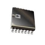
| 描述 | IC DAC 16BIT QUAD 5V 14-TSSOP数模转换器- DAC Quad 16-Bit w/ 10ppm/oC Max |
| DevelopmentKit | EVAL-AD5666EBZ |
| 产品分类 | |
| 品牌 | Analog Devices |
| 产品手册 | |
| 产品图片 |
|
| rohs | 符合RoHS无铅 / 符合限制有害物质指令(RoHS)规范要求 |
| 产品系列 | 数据转换器IC,数模转换器- DAC,Analog Devices AD5666BRUZ-2- |
| 数据手册 | |
| 产品型号 | AD5666BRUZ-2 |
| 产品培训模块 | http://www.digikey.cn/PTM/IndividualPTM.page?site=cn&lang=zhs&ptm=19145http://www.digikey.cn/PTM/IndividualPTM.page?site=cn&lang=zhs&ptm=18614http://www.digikey.cn/PTM/IndividualPTM.page?site=cn&lang=zhs&ptm=26125http://www.digikey.cn/PTM/IndividualPTM.page?site=cn&lang=zhs&ptm=26140http://www.digikey.cn/PTM/IndividualPTM.page?site=cn&lang=zhs&ptm=26150http://www.digikey.cn/PTM/IndividualPTM.page?site=cn&lang=zhs&ptm=26147 |
| 产品种类 | 数模转换器- DAC |
| 位数 | 16 |
| 供应商器件封装 | 14-TSSOP |
| 其它名称 | AD5666BRUZ2 |
| 分辨率 | 16 bit |
| 包装 | 管件 |
| 商标 | Analog Devices |
| 安装类型 | 表面贴装 |
| 安装风格 | SMD/SMT |
| 封装 | Tube |
| 封装/外壳 | 14-TSSOP(0.173",4.40mm 宽) |
| 封装/箱体 | TSSOP-14 |
| 工作温度 | -40°C ~ 105°C |
| 工厂包装数量 | 96 |
| 建立时间 | 6µs |
| 接口类型 | SPI |
| 数据接口 | DSP,MICROWIRE™,QSPI™,串行,SPI™ |
| 最大功率耗散 | 12.5 mW |
| 最大工作温度 | + 105 C |
| 最小工作温度 | - 40 C |
| 标准包装 | 1 |
| 电压参考 | Internal, External |
| 电压源 | 单电源 |
| 电源电压-最大 | 5.5 V |
| 电源电压-最小 | 2.7 V |
| 积分非线性 | +/- 16 LSB |
| 稳定时间 | 6 us |
| 系列 | AD5666 |
| 结构 | Resistor String |
| 转换器数 | 4 |
| 转换器数量 | 4 |
| 输出数和类型 | 4 电压,单极 |
| 输出类型 | Voltage |
| 采样比 | 95 kSPs |
| 采样率(每秒) | - |


- 商务部:美国ITC正式对集成电路等产品启动337调查
- 曝三星4nm工艺存在良率问题 高通将骁龙8 Gen1或转产台积电
- 太阳诱电将投资9.5亿元在常州建新厂生产MLCC 预计2023年完工
- 英特尔发布欧洲新工厂建设计划 深化IDM 2.0 战略
- 台积电先进制程称霸业界 有大客户加持明年业绩稳了
- 达到5530亿美元!SIA预计今年全球半导体销售额将创下新高
- 英特尔拟将自动驾驶子公司Mobileye上市 估值或超500亿美元
- 三星加码芯片和SET,合并消费电子和移动部门,撤换高东真等 CEO
- 三星电子宣布重大人事变动 还合并消费电子和移动部门
- 海关总署:前11个月进口集成电路产品价值2.52万亿元 增长14.8%


PDF Datasheet 数据手册内容提取
Quad, 16-Bit DAC with 5 ppm/°C On-Chip Reference in 14-Lead TSSOP AD5666 FEATURES FUNCTIONAL BLOCK DIAGRAM Low power quad 16-bit DAC VDD VREFIN/VREFOUT 14-lead TSSOP AD5666 1.25V/2.5V REF On-chip 1.25 V/2.5 V, 5 ppm/°C reference LDAC REINGPISUTTER REGDIASCTER SDTARCINAG BUFFER VOUTA Power down to 400 nA @ 5 V, 200 nA @ 3 V SCLK 2.7 V to 5.5 V power supply INTERFACE REINGPISUTTER REGDIASCTER SDTARCINBG BUFFER VOUTB SYNC LOGIC Guaranteed monotonic by design REINGPISUTTER REGDIASCTER SDTARCINCG BUFFER VOUTC DIN Power-on reset to zero scale or midscale REINGPISUTTER REGDIASCTER SDTARCINDG BUFFER VOUTD 3 power-down functions SDO POWER-ON POWER-DOWN HCLaRrd fwunacreti oLDn AtoC pwriotghr LaDmAmCa obvleer croiddee f unction LDAC CLR RPEOSRET LGONGDIC 05298-001 Figure 1. SDO daisy-chaining option Rail-to-rail operation APPLICATIONS Process control Data acquisition systems Portable battery-powered instruments Digital gain and offset adjustment Programmable voltage and current sources Programmable attenuators GENERAL DESCRIPTION The AD5666 is a low power, quad, 16-bit, buffered voltage- The outputs of all DACs can be updated simultaneously using output DAC. The part operates from a single 2.7 V to 5.5 V the LDAC function, with the added functionality of user-select- supply and is guaranteed monotonic by design. able DAC channels to simultaneously update. There is also an asynchronous CLR that clears all DACs to a software-selectable The AD5666 has an on-chip reference with an internal gain of 2. code—0 V, midscale, or full scale. The AD5666-1 has a 1.25 V 5 ppm/°C reference, giving a full-scale output of 2.5 V; the AD5666-2 has a 2.5 V 5 ppm/°C reference, The AD5666 utilizes a versatile 3-wire serial interface that operates giving a full-scale output of 5 V. The on-board reference is off at at clock rates of up to 50 MHz and is compatible with standard power-up, allowing the use of an external reference. The internal SPI®, QSPI™, MICROWIRE™, and DSP interface standards. The reference is turned on by writing to the DAC. on-chip precision output amplifier enables rail-to-rail output swing. The part incorporates a power-on reset circuit that ensures that the DAC output powers up to 0 V (POR pin low) or to midscale PRODUCT HIGHLIGHTS (POR pin high) and remains powered up at this level until a valid 1. Quad, 16-bit DAC. write takes place. The part contains a power-down feature that 2. On-chip 1.25 V/2.5 V, 5 ppm/°C reference. reduces the current consumption of the device to 400 nA at 5 V 3. Available in 14-lead TSSOP. and provides software-selectable output loads while in power-down 4. Selectable power-on reset to 0 V or midscale. mode for any or all DAC channels. 5. Power-down capability. When powered down, the DAC typically consumes 200 nA at 3 V and 400 nA at 5 V. Rev. D Information furnished by Analog Devices is believed to be accurate and reliable. However, no responsibility is assumed by Analog Devices for its use, nor for any infringements of patents or other One Technology Way, P.O. Box 9106, Norwood, MA 02062-9106, U.S.A. rights of third parties that may result from its use. Specifications subject to change without notice. No license is granted by implication or otherwise under any patent or patent rights of Analog Devices. Tel: 781.329.4700 www.analog.com Trademarks and registered trademarks are the property of their respective owners. Fax: 781.461.3113 ©2005–2010 Analog Devices, Inc. All rights reserved.
AD5666 TABLE OF CONTENTS Features .............................................................................................. 1 Resistor String ............................................................................. 20 Applications ....................................................................................... 1 Internal Reference ...................................................................... 20 Functional Block Diagram .............................................................. 1 Output Amplifier ........................................................................ 21 General Description ......................................................................... 1 Serial Interface ............................................................................ 21 Product Highlights ........................................................................... 1 Input Shift Register .................................................................... 22 Revision History ............................................................................... 2 SYNC Interrupt .......................................................................... 22 Specifications ..................................................................................... 3 Daisy-Chaining ........................................................................... 23 AC Characteristics ........................................................................ 7 Internal Reference Register ....................................................... 23 Timing Characteristics ................................................................ 8 Power-On Reset .......................................................................... 23 Absolute Maximum Ratings .......................................................... 10 Power-Down Modes .................................................................. 23 ESD Caution ................................................................................ 10 Clear Code Register ................................................................... 25 Pin Configuration and Function Descriptions ........................... 11 LDAC Function .......................................................................... 25 Typical Performance Characteristics ........................................... 12 Power Supply Bypassing and Grounding ................................ 25 Terminology .................................................................................... 18 Outline Dimensions ....................................................................... 27 Theory of Operation ...................................................................... 20 Ordering Guide .......................................................................... 27 D/A Section ................................................................................. 20 REVISION HISTORY 6/10—Rev. C to Rev. D Changes to Figure 19 and Figure 20 Captions ............................ 14 10/09—Rev. B to Rev. C Changes to Table 7 .......................................................................... 21 2/09—Rev. A to Rev. B Changes to Reference Current Parameter, Table 1 ....................... 3 Changes to Reference Current Parameter, Table 2 ....................... 5 Updated Outline Dimensions ....................................................... 27 11/05—Rev. 0 to Rev. A Change to General Description ...................................................... 1 Change to Specifications .................................................................. 3 10/05—Revision 0: Initial Version Rev. D | Page 2 of 28
AD5666 SPECIFICATIONS V = 4.5 V to 5.5 V, R = 2 kΩ to GND, C = 200 pF to GND, V = V . All specifications T to T , unless otherwise noted. DD L L REFIN DD MIN MAX Table 1. A Grade1 B Grade1 Parameter Min Typ Max Min Typ Max Unit Conditions/Comments STATIC PERFORMANCE2 Resolution 16 16 Bits Relative Accuracy ±32 ±16 LSB See Figure 6 Differential Nonlinearity ±1 ±1 LSB Guaranteed monotonic by design (see Figure 7) Zero-Code Error 1 9 1 9 mV All 0s loaded to DAC register (see Figure 13) Zero-Code Error Drift ±2 ±2 μV/°C Full-Scale Error −0.2 −1 −0.2 −1 % FSR All 1s loaded to DAC register (see Figure 12) Gain Error ±1 ±1 % FSR Gain Temperature Coefficient ±2.5 ±2.5 ppm Of FSR/°C Offset Error ±1 ±9 ±1 ±9 mV DC Power Supply Rejection –80 –80 dB V ± 10% DD Ratio DC Crosstalk 10 10 μV Due to full-scale output change, (External Reference) R = 2 kΩ to GND or V L DD 5 5 μV/mA Due to load current change 10 10 μV Due to powering down (per channel) DC Crosstalk 25 25 μV Due to full-scale output change, (Internal Reference) R = 2 kΩ to GND or V L DD 10 10 μV/mA Due to load current change OUTPUT CHARACTERISTICS3 Output Voltage Range 0 V 0 V V DD DD Capacitive Load Stability 2 2 nF R = ∞ L 10 10 nF R = 2 kΩ L DC Output Impedance 0.5 0.5 Ω Short-Circuit Current 30 30 mA V = 5 V DD Power-Up Time 4 4 μs Coming out of power-down mode V = 5 V DD REFERENCE INPUTS Reference Input Voltage V V V DD DD Reference Current 20 55 20 55 μA V = V = 5.5 V REF DD Reference Input Range 0 V 0 V V DD DD Reference Input Impedance 14.6 14.6 kΩ Per DAC channel REFERENCE OUTPUT Output Voltage 2.495 2.505 2.495 2.505 V At ambient Reference TC3 ±5 ±10 ±5 ±10 ppm/°C Reference Output 7.5 7.5 kΩ Impedance LOGIC INPUTS3 Input Current ±3 ±3 μA All digital inputs Input Low Voltage, V 0.8 0.8 V V = 5 V INL DD Input High Voltage, V 2 2 V V = 5 V INH DD Pin Capacitance 3 3 pF Rev. D | Page 3 of 28
AD5666 A Grade1 B Grade1 Parameter Min Typ Max Min Typ Max Unit Conditions/Comments LOGIC OUTPUTS (SDO)3 Output Low Voltage, V 0.4 0.4 V I = 2 mA OL SINK Output High Voltage, V V − V − I = 2 mA OH DD DD SOURCE 1 1 High Impedance Leakage ±0.25 ±0.25 μA Current High Impedance Output 2 2 pF Capacitance POWER REQUIREMENTS V 4.5 5.5 4.5 5.5 V All digital inputs at 0 or V , DD DD DAC active, excludes load current I (Normal Mode)4 V = V and V = GND DD IH DD IL V = 4.5 V to 5.5 V 0.7 0.9 0.7 0.9 mA Internal reference off DD V = 4.5 V to 5.5 V 1.3 1.6 1.3 1.6 mA Internal reference on DD I (All Power-Down Modes)5 DD V = 4.5 V to 5.5 V 0.4 1 0.4 1 μA V = V and V = GND DD IH DD IL 1 Temperature range is −40°C to +105°C, typical at 25°C. 2 Linearity calculated using a reduced code range of 512 to 65,024. Output unloaded. 3 Guaranteed by design and characterization; not production tested. 4 Interface inactive. All DACs active. DAC outputs unloaded. 5 All four DACs powered down. Rev. D | Page 4 of 28
AD5666 V = 2.7 V to 3.6 V, R = 2 kΩ to GND, C = 200 pF to GND, V = V . All specifications T to T , unless otherwise noted. DD L L REFIN DD MIN MAX Table 2. A Grade1 B Grade1 Parameter Min Typ Max Min Typ Max Unit Conditions/Comments STATIC PERFORMANCE2 Resolution 16 16 Bits Relative Accuracy ±32 ±16 LSB See Figure 5 Differential Nonlinearity ±1 ±1 LSB Guaranteed monotonic by design (see Figure 6) Zero-Code Error 1 9 1 9 mV All 0s loaded to DAC register (see Figure 13) Zero-Code Error Drift ±2 ±2 μV/°C Full-Scale Error −0.2 −1 −0.2 −1 % FSR All 1s loaded to DAC register (see Figure 12) Gain Error ±1 ±1 % FSR Gain Temperature ±2.5 ±2.5 ppm Of FSR/°C Coefficient Offset Error ±1 ±9 ±1 ±9 mV DC Power Supply Rejection –80 –80 dB V ± 10% DD Ratio DC Crosstalk 10 10 μV Due to full-scale output change, (External Reference) R = 2 kΩ to GND or V L DD 5 5 μV/mA Due to load current change 10 10 μV Due to powering down (per channel) DC Crosstalk 25 25 μV Due to full-scale output change, (Internal Reference) R = 2 kΩ to GND or V L DD 10 10 μV/mA Due to load current change OUTPUT CHARACTERISTICS3 Output Voltage Range 0 V 0 V V DD DD Capacitive Load Stability 2 2 nF R = ∞ L 10 10 nF R = 2 kΩ L DC Output Impedance 0.5 0.5 Ω Short-Circuit Current 30 30 mA V = 3 V coming out of power-down mode DD Power-Up Time 4 4 μs Coming out of power-down V = 3 V DD REFERENCE INPUTS Reference Input Voltage V V V DD DD Reference Current 40 55 40 55 μA V = V = 3.6 V REF DD Reference Input Range 0 V 0 V DD DD Reference Input Impedance 14.6 14.6 kΩ Per DAC channel REFERENCE OUTPUT Output Voltage 1.247 1.253 1.247 1.253 V At ambient Reference TC3 ±5 ±15 ±5 ±15 ppm/°C Reference Output 7.5 7.5 kΩ Impedance LOGIC INPUTS3 Input Current ±3 ±3 μA Input Low Voltage, V 0.8 0.8 V V = 3 V INL DD Input High Voltage, V 2 2 V V = 3 V INH DD Pin Capacitance 3 3 pF LOGIC OUTPUTS (SDO)3 Output Low Voltage, V 0.4 0.4 V I = 2 mA OL SINK Output High Voltage, V V − V − I = 2 mA OH DD DD SOURCE 0.5 0.5 High Impedance Leakage ±0.25 ±0.25 μA Current High Impedance Leakage 2 2 pF Rev. D | Page 5 of 28
AD5666 A Grade1 B Grade1 Parameter Min Typ Max Min Typ Max Unit Conditions/Comments Current POWER REQUIREMENTS V 2.7 3.6 2.7 3.6 V All digital inputs at 0 or V , DD DD DAC active, excludes load current I (Normal Mode)4 V = V and V = GND DD IH DD IL V = 2.7 V to 3.6 V 0.65 0.85 0.65 0.85 mA Internal reference off DD V = 2.7 V to 3.6 V 1.3 1.5 1.3 1.5 mA Internal reference on DD I (All Power-Down Modes)5 DD V = 2.7 V to 3.6 V 0.2 1 0.2 1 μA V = V and V = GND DD IH DD IL 1 Temperature range is −40°C to +105°C, typical at 25°C. 2 Linearity calculated using a reduced code range of 512 to 65,024. Output unloaded. 3 Guaranteed by design and characterization; not production tested. 4 Interface inactive. All DACs active. DAC outputs unloaded. 5 All four DACs powered down. Rev. D | Page 6 of 28
AD5666 AC CHARACTERISTICS V =2.7V to 5.5 V, R = 2 kΩ to GND, C = 200 pF to GND, V = V . All specifications T to T , unless otherwise noted. DD L L REFIN DD MIN MAX Table 3. Parameter1, 2 Min Typ Max Unit Conditions/Comments3 Output Voltage Settling Time 6 10 μs ¼ to ¾ scale settling to ±2 LSB Slew Rate 1.5 V/μs Digital-to-Analog Glitch Impulse 4 nV-s 1 LSB change around major carry (see Figure 29) Reference Feedthrough −90 dB V = 2 V ± 0.1 V p-p, frequency = 10 Hz to 20 MHz REF SDO Feedthrough 3 nV-s Daisy-chain mode; SDO load is 10 pF Digital Feedthrough 0.1 nV-s Digital Crosstalk 0.5 nV-s Analog Crosstalk 2.5 nV-s DAC-to-DAC Crosstalk 3 nV-s Multiplying Bandwidth 340 kHz V = 2 V ± 0.2 V p-p REF Total Harmonic Distortion −80 dB V = 2 V ± 0.1 V p-p, frequency = 10 kHz REF Output Noise Spectral Density 120 nV/√Hz DAC code = 0x8400, 1 kHz 100 nV/√Hz DAC code = 0x8400, 10 kHz Output Noise 15 μV p-p 0.1 Hz to 10 Hz 1 Guaranteed by design and characterization; not production tested. 2 See the Terminology section. 3 Temperature range is −40°C to + 105°C, typical at 25°C. Rev. D | Page 7 of 28
AD5666 TIMING CHARACTERISTICS All input signals are specified with tr = tf = 1 ns/V (10% to 90% of V ) and timed from a voltage level of (V + V )/2. See Figure 3 and DD IL IH Figure 5. V = 2.7 V to 5.5 V. All specifications T to T , unless otherwise noted. DD MIN MAX Table 4. Limit at T , T MIN MAX Parameter V = 2.7 V to 5.5 V Unit Conditions/Comments DD t 1 20 ns min SCLK cycle time 1 t 8 ns min SCLK high time 2 t 8 ns min SCLK low time 3 t 13 ns min SYNC to SCLK falling edge set-up time 4 t 4 ns min Data set-up time 5 t 4 ns min Data hold time 6 t 0 ns min SCLK falling edge to SYNC rising edge 7 t 15 ns min Minimum SYNC high time 8 t 13 ns min SYNC rising edge to SCLK fall ignore 9 t 0 ns min SCLK falling edge to SYNC fall ignore 10 t 10 ns min LDAC pulse width low 11 t 15 ns min SCLK falling edge to LDAC rising edge 12 t 5 ns min CLR pulse width low 13 t 0 ns min SCLK falling edge to LDAC falling edge 14 t 300 ns typ CLR pulse activation time 15 t 2, 3 22 ns max SCLK rising edge to SDO valid 16 t 3 5 ns min SCLK falling edge to SYNC rising edge 17 t 3 8 ns min SYNC rising edge to SCLK rising edge 18 t 3 0 ns min SYNC rising edge to LDAC falling edge 19 1 Maximum SCLK frequency is 50 MHz at VDD = 2.7 V to 5.5 V. Guaranteed by design and characterization; not production tested. 2 Measured with the load circuit of Figure 16. t16 determines the maximum SCLK frequency in daisy-chain mode. 3 Daisy-chain mode only. 2mA IOL TO OUTPPUINT VOH(MIN) CL 50pF 2mA IOH 05298-002 Figure 2. Load Circuit for Digital Output (SDO) Timing Specifications Rev. D | Page 8 of 28
AD5666 t10 t1 t 9 SCLK t8 t4 t3 t2 t7 SYNC t 6 t 5 DIN DB31 DB0 t t 11 14 LDAC1 t 12 LDAC2 t 13 CLR 12ASYSNYNCCHHRROONNOOUUS SL DLDAACC U UPDPDAATET EM MOODDEE 05298-003 Figure 3. Serial Write Operation t 1 SCLK 32 64 t7 t4 t3 t2 t17 t18 SYNC t 8 t 9 DIN DB31 DB0 DB31 DB0 INPUT WORD FOR DAC N INPUT WORD FOR DAC N + 1 t 16 SDO DB31 DB0 UNDEFINED INPUT WORD FOR DAC N t 19 t 11 LDAC 05298-004 Figure 4. Daisy-Chain Timing Diagram Rev. D | Page 9 of 28
AD5666 ABSOLUTE MAXIMUM RATINGS T = 25°C, unless otherwise noted. A Table 5. Stresses above those listed under Absolute Maximum Ratings Parameter Rating may cause permanent damage to the device. This is a stress V to GND −0.3 V to +7 V DD rating only; functional operation of the device at these or any Digital Input Voltage to GND −0.3 V to V + 0.3 V DD other conditions above those indicated in the operational V to GND −0.3 V to V + 0.3 V OUT DD section of this specification is not implied. Exposure to absolute V /V to GND −0.3 V to V + 0.3 V REFIN REFOUT DD maximum rating conditions for extended periods may affect Operating Temperature Range device reliability. Industrial −40°C to +105°C Storage Temperature Range −65°C to +150°C Junction Temperature (T ) +150°C JMAX TSSOP Package Power Dissipation (T − T )/θ JMAX A JA θ Thermal Impedance 150.4°C/W JA Reflow Soldering Peak Temperature SnPb 240°C Pb Free 260°C ESD CAUTION ESD (electrostatic discharge) sensitive device. Electrostatic charges as high as 4000 V readily accumulate on the human body and test equipment and can discharge without detection. Although this product features proprietary ESD protection circuitry, permanent damage may occur on devices subjected to high energy electrostatic discharges. Therefore, proper ESD precautions are recommended to avoid performance degradation or loss of functionality. Rev. D | Page 10 of 28
AD5666 PIN CONFIGURATION AND FUNCTION DESCRIPTIONS LDAC 1 14 SCLK SYNC 2 13 DIN VDD 3 AD5666 12 GND VOUTA 4 TOPVIEW 11 VOUTB VOUTC 5 (NottoScale) 10 VOUTD POR 6 9 CLR VREFIN/VREFOUT 7 8 SDO 05298-005 Figure 5. 14-Lead TSSOP (RU-14) Table 6. Pin Function Descriptions Pin No. Mnemonic Description 1 LDAC Pulsing this pin low allows any or all DAC registers to be updated if the input registers have new data. This allows all DAC outputs to simultaneously update. Alternatively, this pin can be tied permanently low. 2 SYNC Active Low Control Input. This is the frame synchronization signal for the input data. When SYNC goes low, it powers on the SCLK and DIN buffers and enables the input shift register. Data is transferred in on the falling edges of the next 32 clocks. If SYNC is taken high before the 32nd falling edge, the rising edge of SYNC acts as an interrupt and the write sequence is ignored by the device. 3 V Power Supply Input. These parts can be operated from 2.7 V to 5.5 V, and the supply should be decoupled DD with a 10 μF capacitor in parallel with a 0.1 μF capacitor to GND. 4 V A Analog Output Voltage from DAC A. The output amplifier has rail-to-rail operation. OUT 5 V C Analog Output Voltage from DAC C. The output amplifier has rail-to-rail operation. OUT 6 POR Power-on Reset Pin. Tying this pin to GND powers up the part to 0 V. Tying this pin to V powers up DD the part to midscale. 7 V /V The AD5666 has a common pin for reference input and reference output. When using the internal REFIN REFOUT reference, this is the reference output pin. When using an external reference, this is the reference input pin. The default for this pin is as a reference input. 8 SDO Serial Data Output. Can be used for daisy-chaining a number of these devices together or for reading back the data in the shift register for diagnostic purposes. The serial data is transferred on the rising edge of SCLK and is valid on the falling edge of the clock. 9 CLR Asynchronous Clear Input. The CLR input is falling edge sensitive. When CLR is low, all LDAC pulses are ignored. When CLR is activated, the input register and the DAC register are updated with the data contained in the CLR code register—zero, midscale, or full scale. Default setting clears the output to 0 V. 10 V D Analog Output Voltage from DAC D. The output amplifier has rail-to-rail operation. OUT 11 V B Analog Output Voltage from DAC B. The output amplifier has rail-to-rail operation. OUT 12 GND Ground Reference Point for All Circuitry on the Part. 13 DIN Serial Data Input. This device has a 32-bit shift register. Data is clocked into the register on the falling edge of the serial clock input. 14 SCLK Serial Clock Input. Data is clocked into the input shift register on the falling edge of the serial clock input. Data can be transferred at rates of up to 50 MHz. Rev. D | Page 11 of 28
AD5666 TYPICAL PERFORMANCE CHARACTERISTICS 1.0 10 VDD=5V 8 VTADD==25V°RCEF=5V 00..86 VTARE=FO2U5T°C=2.5V 6 0.4 B) 4 S R (LSB) 2 RROR (L 0.02 O 0 E RR NL –0.2 L E –2 D –0.4 N I –4 –0.6 –1––0680 5k 10k 15k 20k 25k 30k 35k 40k 45k 50k 55k 60k 65k05298-006 ––10..080 5000 10000 15000 20000 25000 30000 35000 40000 45000 50000 55000 60000 6500005298-009 CODE CODE Figure 6. INL Figure 9. DNL—AD5666-2 10 10..08 VTADD==25V°RCEF=5V 86 VVTADRDE=F=O25U3°TVC=1.25V 0.6 4 B) SB) 0.4 R (LS 2 L ERROR (L –00..220 INL ERRO ––420 N D –0.4 –6 –––010...6080 10k 20k 30k 40k 50k 60k 05298-007 –1–080 5000 10000 15000 20000 25000 30000 35000 40000 45000 50000 55000 60000 6500005298-010 CODE CODE Figure 7. DNL Figure 10. INL—AD5666-1 10 1.0 VDD=5V VDD=3V 8 VREFOUT=2.5V 0.8 VREFOUT=1.25V TA=25°C TA=25°C 6 0.6 INL ERROR (LSB) ––42042 DNL ERROR (LSB) ––0000....42420 –6 –0.6 –1–08 05298-008 ––01..80 05298-011 0 5000 10000 15000 20000 25000 30000 35000 40000 45000 50000 55000 60000 65000 0 5000 10000 15000 20000 25000 30000 35000 40000 45000 50000 55000 60000 65000 CODE CODE Figure 8. INL—AD5666-2 Figure 11. DNL—AD5666-1 Rev. D | Page 12 of 28
AD5666 0 1.0 VDD = 5V TA=25°C –0.02 0.5 ZERO-SCALEERROR –0.04 GAIN ERROR 0 –0.06 SR) –0.08 V) F m –0.5 R (% –0.10 OR ( RRO –0.12 ERR –1.0 E –0.14 FULL-SCALE ERROR –1.5 –0.16 ––00..1280 05298-030 ––22..05 OFFSETERROR 05298-045 –40 –20 0 20 40 60 80 100 2.7 3.2 3.7 4.2 4.7 5.2 TEMPERATURE (°C) VDD(V) Figure 12. Gain Error and Full-Scale Error vs. Temperature Figure 15. Zero-Scale Error and Offset Error vs. Supply Voltage 1.5 3.5 VDD=3.6V VDD=5.5V 1.0 ZERO-SCALEERROR 3.0 0.5 2.5 mV) 0 NCY 2.0 R ( –0.5 UE O Q R E 1.5 R R E –1.0 F 1.0 –1.5 OFFSETERROR 0.5 ––22..05–40 –20 0 20 40 60 80 100 05298-021 00.62 0.63 0.64 0.65 0.66 0.67 0.68 0.69 0.7 0.71 0.7205298-028 TEMPERATURE(°C) IDD(mA) Figure 13. Zero-Scale Error and Offset Error vs. Temperature Figure 16. IDD Histogram with External Reference 1.0 2.5 VDD=3.6V VDD=5.5V 0.5 2.0 GAINERROR % FSR) 0 FULL-SCALEERROR ENCY 1.5 R ( –0.5 QU O E R R 1.0 R F E –1.0 0.5 –1.5 –2.0 05298-031 0 05298-029 2.7 3.2 3.7 4.2 4.7 5.2 1.26 1.28 1.30 1.32 1.34 1.36 1.38 VDD(V) IDD(mA) Figure 14. Gain Error and Full-Scale Error vs. Supply Voltage Figure 17. IDD Histogram with Internal Reference Rev. D | Page 13 of 28
AD5666 0.50 1.0 DACLOADEDWITH DACLOADEDWITH TA=25°C VDD=VREF=5V 0.40 FULL-SCALE ZERO-SCALE 0.9 SOURCINGCURRENT SINKINGCURRENT 0.30 0.8 V) 0.20 0.7 GE ( 0.10 VDD=3V 0.6 VOLTA 0 VREFOUT=1.25V (mA)D 0.5 VDD=VREF=3V OR –0.10 ID 0.4 R R E –0.20 0.3 –0.30 VDD=5V 0.2 VREFOUT=2.5V ––00..5400 05298-019 0.10 05298-014 –10 –8 –6 –4 –2 0 2 4 6 8 10 512 10512 20512 30512 40512 50512 60512 CURRENT(mA) CODE Figure 18. Headroom at Rails vs. Source and Sink Figure 21. Supply Current vs. Code 6.00 1.0 VDD=5V FULLSCALE 5.00 VTARE=FO25U°TC=2.5V 0.9 VDD=VREFIN=5.5V 0.8 4.00 3/4SCALE 0.7 0.6 V (V)OUT 32..0000 MIDSCALE I (mA)DD 00..54 VDD=VREFIN=3.6V 1/4SCALE 1.00 0.3 0.2 –1.000 ZEROSCALE 05298-012 0.01 05298-015 –30 –20 –10 0 10 20 30 –40 –20 0 20 40 60 80 100 CURRENT(mA) TEMPERATURE(°C) Figure 19. Source and Sink Current Capability with VDD = 5 V Figure 22. Supply Current vs. Temperature 4.00 1.0 VVDRDEF=OU3VT=1.25V 0.9 TA=25°C 3.00 TA=25°C 0.8 FULLSCALE 0.7 2.00 3/4SCALE 0.6 V) A) V (OUT 1.00 MIDSCALE I (mDD 00..54 1/4SCALE 0.3 0 ZEROSCALE 0.2 –1.00 05298-013 0.10 05298-016 –30 –20 –10 0 10 20 30 2.7 3.2 3.7 4.2 4.7 5.2 CURRENT(mA) VDD(V) Figure 20. Source and Sink Current Capability with VDD = 3 V Figure 23. Supply Current vs. Supply Voltage Rev. D | Page 14 of 28
AD5666 4.0 TA=25°C VDD=VREF=5V 3.5 TA=25°C 3.0 2.5 A) VDD (mD 2.0 1 D I 1.5 VDD=5V 1.0 0.050 VDD1=3V 2 3 4 5 605298-017 2 CH12.0VVOUTCH2 1.0V M100μs125MS/s 8.0ns/pt 05298-033 VLOGIC(V) ACH1 1.28V Figure 24. Supply Current vs. Logic Input Voltage Figure 27. Power-On Reset to Midscale SYNC 1 SLCK 3 VDD=VREF=5V TA=25°C FULL-SCALECODECHANGE 0x0000TO0xFFFF OUTPUTLOADEDWITH2kΩ AND200pFTO GND VOUT=909mV/DIV VOUT VDD = 5V 1 05298-018 2 CH1 5.0V CH2 500mV M400ns A CH1 1.4V 05298-034 TIMEBASE=4μs/DIV CH3 5.0V Figure 25. Full-Scale Settling Time Figure 28. Exiting Power-Down to Midscale 2.505 VTADD==25V°RCEF=5V 222...555000234 VVTADRDE=F=O25U5°TVC=2.5V 2.501 4ns/SAMPLENUMBER 2.500 GLITCH IMPULSE=3.55nV-s 2.499 1LSBCHANGEAROUND 2.498 MIDSCALE(0x8000TO0x7FFF) 2.497 V) 2.496 (UT 2.495 O 2.494 VDD V 2.493 1 2.492 2.491 2.490 MAX(C2)* 2.489 420.0mV 2.488 2 VOUT 05298-020 222...444888567 05298-022 CH12.0V CH2 500mV M100μs125MS/s 8.0ns/pt 0 64 128 192 256 320 384 448 512 ACH1 1.28V SAMPLE Figure 26. Power-On Reset to 0 V Figure 29. Digital-to-Analog Glitch Impulse Rev. D | Page 15 of 28
AD5666 2.5000 2.4995 VDD=5V VREFOUT=2.5V 2.4990 TA=25°C DAC LOADED WITHMIDSCALE 2.4985 2.4980 (V)OUT 2.4975 V/DIV1 V 2.4970 0μ 1 2.4965 2.4960 VDD=5V 22..449955050 64 128 192 256 3VT42nAR0sE=/FSO2A5UM°T3CP8=4L2E.5NVU4M48BER51205298-035 05298-038 SAMPLE 5s/DIV Figure 30. Analog Crosstalk Figure 33. 0.1 Hz to 10 Hz Output Noise Plot, Internal Reference 2.4900 2.4895 VDD=3V VREFOUT=1.25V 2.4890 TDAAC= 2L5O°ACDED WITHMIDSCALE 2.4885 V) 2.4880 V (OUT 2.4875 V/DIVμ1 5 2.4870 2.4865 VDD=5V 22..448856500 64 128 192 256 3VT42nAR0sE=/FSO2A5UM°T3CP8=4L2E.5NVU4M48BER51205298-036 05298-039 SAMPLE 4s/DIV Figure 31. DAC-to-DAC Crosstalk Figure 34. 0.1 Hz to 10 Hz Output Noise Plot, Internal Reference 800 TA=25°C MIDSCALELOADED 700 VDD=VREF=5V TA=25°C DACLOADEDWITHMIDSCALE Hz) 600 (cid:0) V/ 500 n E ( S OI 400 N 1 PUT 300 UT VDD=5V O 200 VREFOUT=2.5V YXAAXXIISS==24μsV/D/DIVIV 05298-037 1000100VVDRDEF=OU3VT=11.02050V FREQU10E0N0C0Y(Hz) 100000 1000005298-04000 Figure 32. 0.1 Hz to 10 Hz Output Noise Plot, External Reference Figure 35. Noise Spectral Density, Internal Reference Rev. D | Page 16 of 28
AD5666 –20 VDD=5V –30 TA=25°C DACLOADEDWITHFULLSCALE CLR VREF=2V±0.3Vp-p 3 –40 –50 VOUTF dB) –60 ( –70 –80 VOUTB –1–0900 2k 4k 6k 8k 10k05298-041 424 CH2 1.0V M200ns ACH3 1.10V 05298-043 FREQUENCY(Hz) CH35.0V CH4 1.0V Figure 36. Total Harmonic Distortion Figure 38. Hardware CLR 16 5 VTARE=F2=5°VCDD 0 TVADD==255°VC 14 –5 VDD=3V 12 –10 s) –15 ME (μ 10 (dB) –20 TI 8 VDD=5V –25 –30 6 4 05298-042 ––4305 05298-044 0 1 2 3 4 5 6 7 8 9 10 10k 100k 1M 10M CAPACITANCE(nF) FREQUENCY(Hz) Figure 37. Settling Time vs. Capacitive Load Figure 39. Multiplying Bandwidth Rev. D | Page 17 of 28
AD5666 TERMINOLOGY Relative Accuracy Full-Scale Error For the DAC, relative accuracy, or integral nonlinearity (INL), is Full-scale error is a measure of the output error when full-scale a measure of the maximum deviation in LSBs from a straight code (0xFFFF) is loaded into the DAC register. Ideally, the line passing through the endpoints of the DAC transfer output should be V − 1 LSB. Full-scale error is expressed as a DD function. Figure 6 shows a plot of typical INL vs. code. percentage of the full-scale range. Figure 13 shows a plot of typical full-scale error vs. temperature. Differential Nonlinearity Differential nonlinearity (DNL) is the difference between the Digital-to-Analog Glitch Impulse measured change and the ideal 1 LSB change between any two Digital-to-analog glitch impulse is the impulse injected into the adjacent codes. A specified differential nonlinearity of ±1 LSB analog output when the input code in the DAC register changes maximum ensures monotonicity. This DAC is guaranteed mono- state. It is normally specified as the area of the glitch in nV-s tonic by design. Figure 7 shows a plot of typical DNL vs. code. and is measured when the digital input code is changed by 1 LSB at the major carry transition (0x7FFF to 0x8000). See Offset Error Figure 29. Offset error is a measure of the difference between the actual V and the ideal V , expressed in millivolts in the linear OUT OUT DC Power Supply Rejection Ratio (PSRR) region of the transfer function. Offset error is measured on the PSRR indicates how the output of the DAC is affected by changes AD5666 with Code 512 loaded into the DAC register. It can be in the supply voltage. PSRR is the ratio of the change in V to OUT negative or positive and is expressed in millivolts. a change in V for full-scale output of the DAC. It is measured DD in decibels. V is held at 2 V, and V is varied ±10%. Zero-Code Error REF DD Zero-code error is a measure of the output error when zero DC Crosstalk code (0x0000) is loaded into the DAC register. Ideally, the DC crosstalk is the dc change in the output level of one DAC in output should be 0 V. The zero-code error is always positive in response to a change in the output of another DAC. It is measured the AD5666, because the output of the DAC cannot go below 0 V. with a full-scale output change on one DAC (or soft power-down It is due to a combination of the offset errors in the DAC and and power-up) while monitoring another DAC kept at midscale. output amplifier. Zero-code error is expressed in millivolts. It is expressed in microvolts. Figure 13 shows a plot of typical zero-code error vs. DC crosstalk due to load current change is a measure of the temperature. impact that a change in load current on one DAC has to another Gain Error DAC kept at midscale. It is expressed in microvolts per milliamp. Gain error is a measure of the span error of the DAC. It is the Reference Feedthrough deviation in slope of the DAC transfer characteristic from the Reference feedthrough is the ratio of the amplitude of the signal ideal, expressed as a percentage of the full-scale range. at the DAC output to the reference input when the DAC output is not being updated (that is, LDAC is high). It is expressed in Zero-Code Error Drift decibels. Zero-code error drift is a measure of the change in zero-code error with a change in temperature. It is expressed in μV/°C. Digital Feedthrough Digital feedthrough is a measure of the impulse injected into Gain Error Drift the analog output of a DAC from the digital input pins of the Gain error drift is a measure of the change in gain error with device, but is measured when the DAC is not being written to changes in temperature. It is expressed in (ppm of full-scale (SYNC held high). It is specified in nV-s and measured with a range)/°C. full-scale change on the digital input pins, that is, from all 0s to all 1s or vice versa. Rev. D | Page 18 of 28
AD5666 Digital Crosstalk Multiplying Bandwidth Digital crosstalk is the glitch impulse transferred to the output The amplifiers within the DAC have a finite bandwidth. The of one DAC at midscale in response to a full-scale code change multiplying bandwidth is a measure of this. A sine wave on the (all 0s to all 1s or vice versa) in the input register of another reference (with full-scale code loaded to the DAC) appears on DAC. It is measured in standalone mode and is expressed in the output. The multiplying bandwidth is the frequency at nV-s. which the output amplitude falls to 3 dB below the input. Analog Crosstalk Total Harmonic Distortion (THD) Analog crosstalk is the glitch impulse transferred to the output Total harmonic distortion is the difference between an ideal of one DAC due to a change in the output of another DAC. It is sine wave and its attenuated version using the DAC. The sine measured by loading one of the input registers with a full-scale wave is used as the reference for the DAC, and the THD is a code change (all 0s to all 1s or vice versa) while keeping LDAC measure of the harmonics present on the DAC output. It is high, and then pulsing LDAC low and monitoring the output of measured in decibels. the DAC whose digital code has not changed. The area of the glitch is expressed in nV-s. DAC-to-DAC Crosstalk DAC-to-DAC crosstalk is the glitch impulse transferred to the output of one DAC due to a digital code change and subsequent output change of another DAC. This includes both digital and analog crosstalk. It is measured by loading one of the DACs with a full-scale code change (all 0s to all 1s or vice versa) with LDAC low and monitoring the output of another DAC. The energy of the glitch is expressed in nV-s. Rev. D | Page 19 of 28
AD5666 THEORY OF OPERATION D/A SECTION R The AD5666 DAC is fabricated on a CMOS process. The archi- tecture consists of a string of DACs followed by an output buffer amplifier. The parts include an internal 1.25 V/2.5 V, 5 ppm/°C R reference with an internal gain of 2. Figure 40 shows a block diagram of the DAC architecture. R TO OUTPUT AMPLIFIER VDD REF(+) RESISTOR DACREGISTER STRING VOUT REF(–) OUTPUT R AMPLIFIER GND (GAIN=+2) 05298-023 R Figure 40. DAC Architecture 05298-024 Because the input coding to the DAC is straight binary, the ideal Figure 41. Resistor String output voltage when using an external reference is given by INTERNAL REFERENCE ⎛ D ⎞ V =V ×⎜ ⎟ OUT REFIN ⎝2N ⎠ The AD5666 has an on-chip reference with an internal gain of 2. The AD5666-1 has a 1.25 V 5 ppm/°C reference, giving a full-scale The ideal output voltage when using and internal reference is output of 2.5 V. The AD5666-2 has a 2.5 V 5 ppm/°C reference, given by giving a full-scale output of 5 V. The on-board reference is off at ⎛ D ⎞ power-up, allowing the use of an external reference. The internal VOUT =2×VREFOUT×⎜⎝2N ⎟⎠ reference is enabled via a write to a control register. The internal reference associated with each part is available at where: the V pin. A buffer is required if the reference output is D = decimal equivalent of the binary code that is loaded to the REFOUT used to drive external loads. When using the internal reference, DAC register. it is recommended that a 100 nF capacitor be placed between 0 to 65,535 for AD5666 (16 bits). the reference output and GND for reference stability. N = the DAC resolution. RESISTOR STRING Individual channel power-down is not supported while using the internal reference. The resistor string section is shown in Figure 41. It is simply a string of resistors, each of value R. The code loaded into the DAC register determines at which node on the string the voltage is tapped off to be fed into the output amplifier. The voltage is tapped off by closing one of the switches connecting the string to the amplifier. Because it is a string of resistors, it is guaranteed monotonic. Rev. D | Page 20 of 28
AD5666 OUTPUT AMPLIFIER Table 7. Command Definitions Command The output buffer amplifier can generate rail-to-rail voltages on C3 C2 C1 C0 Description its output, which gives an output range of 0 V to V . The DD 0 0 0 0 Write to Input Register n amplifier is capable of driving a load of 2 kΩ in parallel with 0 0 0 1 Update DAC Register n 1000 pF to GND. The source and sink capabilities of the output 0 0 1 0 Write to Input Register n, update all amplifier can be seen in Figure 19 and Figure 20. The slew rate (software LDAC) is 1.5 V/μs with a ¼ to ¾ scale settling time of 10 μs. 0 0 1 1 Write to and update DAC Channel n SERIAL INTERFACE 0 1 0 0 Power down/power up DAC 0 1 0 1 Load clear code register The AD5666 has a 3-wire serial interface (SYNC, SCLK, and 0 1 1 0 Load LDAC register DIN) that is compatible with SPI, QSPI, and MICROWIRE 0 1 1 1 Reset (power-on reset) interface standards as well as most DSPs. See Figure 3 for a 1 0 0 0 Set up DCEN/REF register timing diagram of a typical write sequence. 1 0 0 1 No operation The write sequence begins by bringing the SYNC line low. Data – – – – Reserved from the DIN line is clocked into the 32-bit shift register on the 1 1 1 1 Reserved falling edge of SCLK. The serial clock frequency can be as high as 50 MHz, making the AD5666 compatible with high speed Table 8. Address Commands DSPs. On the 32nd falling clock edge, the last data bit is clocked Address (n) in and the programmed function is executed, that is, a change Selected DAC in DAC register contents and/or a change in the mode of A3 A2 A1 A0 Channel operation. At this stage, the SYNC line can be kept low or be 0 0 0 0 DAC A brought high. In either case, it must be brought high for a 0 0 0 1 DAC B minimum of 15 ns before the next write sequence so that a 0 0 1 0 DAC C falling edge of SYNC can initiate the next write sequence. 0 0 1 1 DAC D Because the SYNC buffer draws more current when VIN = 2 V 1 1 1 1 All DACs than it does when V = 0.8 V, SYNC should be idled low IN between write sequences for even lower power operation of the part. As is mentioned previously, however, SYNC must be brought high again just before the next write sequence. Rev. D | Page 21 of 28
AD5666 INPUT SHIFT REGISTER SYNC INTERRUPT The input shift register is 32 bits wide (see Figure 42). The first In a normal write sequence, the SYNC line is kept low for at four bits are don’t cares. The next four bits are the command least 32 falling edges of SCLK, and the DAC is updated on the bits, C3 to C0 (see Table 8), followed by the 4-bit DAC address 32nd falling edge. However, if SYNC is brought high before the bits, A3 to A0 (see Table 9) and finally the 16-bit data-word. 32nd falling edge, this acts as an interrupt to the write sequence. The data-word comprises the 16-bit input code followed by four The shift register is reset, and the write sequence is seen as don’t care bits for the AD5666 (see Figure 42). These data bits invalid. Neither an update of the DAC register contents nor a are transferred to the DAC register on the 32nd falling edge of change in the operating mode occurs (see Figure 43). SCLK. DB31(MSB) DB0(LSB) X X X X C3 C2 C1 C0 A3 A2 A1 A0 D15 D14 D13 D12 D11 D10 D9 D8 D7 D6 D5 D4 D3 D2 D1 D0 X X X X DATABITS COMMANDBITS ADDRESSBITS 05298-025 Figure 42. AD5666 Input Register Content SCLK SYNC DIN DB31 DB0 DB31 DB0 SYNCHINIGVHALBIEDFWORREITE32SNEDQFUAELNLCINEG: EDGE VALIDWORNITTEHSEE3Q2UNEDNFCAEL, LOINUGTPEUDTGUEPDATES 05298-026 Figure 43. SYNC Interrupt Facility Rev. D | Page 22 of 28
AD5666 DAISY-CHAINING POWER-ON RESET For systems that contain several DACs, or where the user The AD5666 contains a power-on reset circuit that controls the wishes to read back the DAC contents for diagnostic purposes, output voltage during power-up. By connecting the POR pin the SDO pin can be used to daisy-chain several devices together low, the AD5666 output powers up to 0 V; by connecting the and provide serial readback. POR pin high, the AD5666 output powers up to midscale. The output remains powered up at this level until a valid write The daisy-chain mode is enabled through a software executable sequence is made to the DAC. This is useful in applications DCEN command. Command 1000 is reserved for this DCEN where it is important to know the state of the output of the DAC function (see Table 7). The daisy-chain mode is enabled by while it is in the process of powering up. There is also a software setting a bit (DB1) in the DCEN register. The default setting is executable reset function that resets the DAC to the power-on standalone mode, where Bit DCEN = 0. Table 9 shows how the reset code. Command 0111 is reserved for this reset function state of the bits corresponds to the mode of operation of the (see Table 7). Any events on LDAC or CLR during power-on device. reset are ignored. The SCLK is continuously applied to the input shift register POWER-DOWN MODES when SYNC is low. If more than 32 clock pulses are applied, the The AD5666 contains four separate modes of operation. data ripples out of the shift register and appears on the SDO Command 0100 is reserved for the power-down function (see line. This data is clocked out on the rising edge of SCLK and is Table 7). These modes are software-programmable by setting valid on the falling edge. By connecting this line to the DIN two bits, Bit DB19 and Bit DB18, in the control register. Table 11 input on the next DAC in the chain, a multi-DAC interface is shows how the state of the bits corresponds to the mode of constructed. Each DAC in the system requires 32 clock pulses; operation of the device. Any or all DACs (DAC D to DAC A) therefore, the total number of clock cycles must equal 32N, can be powered down to the selected mode by setting the cor- where N is the total number of devices in the chain. responding four bits (DB7, DB6, DB1, DB0) to 1. See Table 12 for the contents of the input shift register during power-down/ When the serial transfer to all devices is complete, SYNC is power-up operation. When using the internal reference, only taken high. This prevents any further data from being clocked all channel power-down to the selected modes is supported. into the input shift register. When both bits are set to 0, the part works normally with its If SYNC is taken high before 32 clocks are clocked into the part, normal power consumption of 700 μA at 5 V. However, for the it is considered an invalid frame and the data is discarded. three power-down modes, the supply current falls to 400 nA at The serial clock can be continuous or a gated clock. A con- 5 V (200 nA at 3 V). Not only does the supply current fall, but tinuous SCLK source can be used only if the SYNC can be held the output stage is also internally switched from the output of the amplifier to a resistor network of known values. This has the low for the correct number of clock cycles. In gated clock mode, advantage that the output impedance of the part is known while a burst clock containing the exact number of clock cycles must the part is in power-down mode. There are three different be used, and SYNC must be taken high after the final clock to options. The output is connected internally to GND through latch the data. either a 1 kΩ or a 100 kΩ resistor, or it is left open-circuited INTERNAL REFERENCE REGISTER (three-state). The output stage is illustrated in Figure 44. The on-board reference is off at power-up by default. This The bias generator, output amplifier, resistor string, and other allows the use of an external reference if the application requires associated linear circuitry are shut down when the power-down it. The on-board reference can be turned on/off by a user- mode is activated. The internal reference is powered down only programmable REF register by setting Bit DB0 high or low (see when all channels are powered down. However, the contents of Table 9). Command 1000 is reserved for this internal REF set- the DAC register are unaffected when in power-down. The time up command (see Table 7). Table 11 shows how the state of the to exit power-down is typically 4 μs for V = 5 V and for DD bits in the input shift register corresponds to the mode of V = 3 V (see Figure 28). DD operation of the device. Any combination of DACs can be powered up by setting PD1 and PD0 to 0 (normal operation). The output powers up to the value in the input register (LDAC Low) or to the value in the DAC register before powering down (LDAC high). Rev. D | Page 23 of 28
AD5666 Table 9. Daisy-Chain Enable/In ternal Reference Register DCEN (DB1) REF (DB0) Action 0 0 Standalone mode, reference off (default) 0 1 Standalone mode, reference on 1 0 DCEN mode, reference off 1 1 DCEN mode, reference on Table 10. 32-Bit Input Shift Register Contents for Daisy-Chain Enable and Reference Set-Up Function MSB LSB DB31 to DB28 DB27 DB26 DB25 DB24 DB23 DB22 DB21 DB20 DB19 to DB2 DB1 DB0 X 1 0 0 0 X X X X X 1/0 1/0 Don’t cares Command bits (C3 to C0) Address bits (A3 to A0) Don’t cares DCEN/REF register Table 11. Modes of Operation DB9 DB8 Operating Mode 0 0 Normal operation Power-down modes 0 1 1 kΩ to GND 1 0 100 kΩ to GND 1 1 Three-state Table 12. 32-Bit Input Shift Register Contents for Power-Up/Power-Down Function MSB LSB DB31 to DB19 to DB7 to DB28 DB27 DB26 DB25 DB24 DB23 DB22 DB21 DB20 DB10 DB9 DB8 DB4 DB3 DB2 DB1 DB0 X 0 1 0 0 X X X X X PD1 PD0 X DAC D DAC C DAC B DAC A Don’t Command bits (C2 to C0) Address bits (A3 to A0)— Don’t Power-down Don’t Power-down/power-up channel selection— cares don’t cares cares mode cares set bit to 1 to select SRTERSINISGTDOARC AMPLIFIER VOUT POWER-DOWN CIRCUITRY RESISTOR NETWORK 05298-027 Figure 44. Output Stage During Power-Down Rev. D | Page 24 of 28
AD5666 CLEAR CODE REGISTER updates synchronously; that is, the DAC register is updated after new data is read, regardless of the state of the LDAC pin. The AD5666 has a hardware CLR pin that is an asynchronous It effectively sees the LDAC pin as being tied low. (See Table 15 clear input. The CLR input is falling edge sensitive. Bringing the for the LDAC register mode of operation.) This flexibility is CLR line low clears the contents of the input register and the useful in applications where the user wants to simultaneously DAC registers to the data contained in the user-configurable update select channels while the rest of the channels are CLR register and sets the analog outputs accordingly. This synchronously updating. function can be used in system calibration to load zero scale, midscale, or full scale to all channels together. These clear code Writing to the DAC using command 0110 loads the 4-bit LDAC values are user-programmable by setting two bits, Bit DB1 and register (DB3 to DB0). The default for each channel is 0; that is, Bit DB0, in the control register (see Table 13). The default the LDAC pin works normally. Setting the bits to 1 means the setting clears the outputs to 0 V. Command 0101 is reserved for DAC channel is updated regardless of the state of the LDAC loading the clear code register (see Table 7). pin. See Table 16 for the contents of the input shift register during the load LDAC register mode of operation. The part exits clear code mode on the 32nd falling edge of the next write to the part. If CLR is activated during a write POWER SUPPLY BYPASSING AND GROUNDING sequence, the write is aborted. When accuracy is important in a circuit, it is helpful to carefully The CLR pulse activation time—the falling edge of CLR to when consider the power supply and ground return layout on the the output starts to change—is typically 280 ns. However, if outside board. The printed circuit board containing the AD5666 should the DAC linear region, it typically takes 520 ns after executing have separate analog and digital sections. If the AD5666 is in a CLR for the output to start changing (see Figure 38). system where other devices require an AGND-to-DGND connection, the connection should be made at one point only. See Table 14 for contents of the input shift register during the This ground point should be as close as possible to the AD5666. loading clear code register operation The power supply to the AD5666 should be bypassed with 10 μF LDAC FUNCTION and 0.1 μF capacitors. The capacitors should physically be as close as possible to the device, with the 0.1 μF capacitor ideally The outputs of all DACs can be updated simultaneously using right up against the device. The 10 μF capacitors are the the hardware LDAC pin. tantalum bead type. It is important that the 0.1 μF capacitor has Synchronous LDAC: After new data is read, the DAC registers low effective series resistance (ESR) and low effective series inductance (ESI), such as is typical of common ceramic types of are updated on the falling edge of the 32nd SCLK pulse. LDAC capacitors. This 0.1 μF capacitor provides a low impedance path can be permanently low or pulsed as in Figure 3. to ground for high frequencies caused by transient currents due Asynchronous LDAC: The outputs are not updated at the same to internal logic switching. time that the input registers are written to. When LDAC goes The power supply line should have as large a trace as possible to low, the DAC registers are updated with the contents of the provide a low impedance path and reduce glitch effects on the input register. supply line. Clocks and other fast switching digital signals should be shielded from other parts of the board by digital Alternatively, the outputs of all DACs can be updated ground. Avoid crossover of digital and analog signals if possible. simultaneously using the software LDAC function by writing to When traces cross on opposite sides of the board, ensure that Input Register n and updating all DAC registers. Command they run at right angles to each other to reduce feedthrough 0011 is reserved for this software LDAC function. effects through the board. The best board layout technique is An LDAC register gives the user extra flexibility and control the microstrip technique, where the component side of the board is dedicated to the ground plane only and the signal over the hardware LDAC pin. This register allows the user to traces are placed on the solder side. However, this is not always select which combination of channels to simultaneously update possible with a 2-layer board. when the hardware LDAC pin is executed. Setting the LDAC bit register to 0 for a DAC channel means that this channel’s update is controlled by the LDAC pin. If this bit is set to 1, this channel Rev. D | Page 25 of 28
AD5666 Table 13. Clear Code Register Clear Code Register DB1 DB0 CR1 CR0 Clears to Code 0 0 0x0000 0 1 0x8000 1 0 0xFFFF 1 1 No operation Table 14. 32-Bit Input Shift Register Contents for Clear Code Function MSB LSB DB31 to DB28 DB27 DB26 DB25 DB24 DB23 DB22 DB21 DB20 DB19 to DB2 DB1 DB0 X 0 1 0 1 X X X X X 1/0 1/0 Don’t cares Command bits (C3 to C0) Address bits (A3 to A0) Don’t cares Clear code register (CR1 to CR0) Table 15. LDAC Overwrite Definition Load DAC Register LDAC Bits (DB3 to DB0) LDAC Pin LDAC Operation 0 1/0 Determined by LDAC pin 1 X—don’t care DAC channels update, overrides the LDAC pin. DAC channels see LDAC as 0. Table 16. 32-Bit Input Shift Register Contents for LDAC Overwrite Function MSB LSB DB31 DB19 to to DB28 DB27 DB26 DB25 DB24 DB23 DB22 DB21 DB20 DB4 DB3 DB2 DB1 DB0 X 0 1 1 0 X X X X X DAC D DAC C DAC B DAC A Don’t Command bits (C3 to C0) Address bits (A3 to A0)— Don’t Setting LDAC bit to 1 override LDAC pin cares don’t cares cares Rev. D | Page 26 of 28
AD5666 OUTLINE DIMENSIONS 5.10 5.00 4.90 14 8 4.50 4.40 6.40 BSC 4.30 1 7 PIN 1 0.65 BSC 1.05 1.00 1M.2A0X 0.20 0.80 0.09 0.75 0.15 8° 0.60 0.05 0.30 SPLEAATNIENG 0° 0.45 COPLANARITY 0.19 0.10 COMPLIANT TO JEDEC STANDARDS MO-153-AB-1 061908-A Figure 45. 14-Lead Thin Shrink Small Outline Package [TSSOP] (RU-14) Dimensions shown in millimeters ORDERING GUIDE Package Power-On Internal Model1 Temperature Range Package Description Option Reset to Code Accuracy Reference AD5666BRUZ-1 −40°C to +105°C 14-Lead TSSOP RU-14 Zero ±16 LSB INL 1.25 V AD5666BRUZ-1REEL7 −40°C to +105°C 14-Lead TSSOP RU-14 Zero ±16 LSB INL 1.25 V AD5666BRUZ-2 −40°C to +105°C 14-Lead TSSOP RU-14 Zero ±16 LSB INL 2.5 V AD5666BRUZ-2REEL7 −40°C to +105°C 14-Lead TSSOP RU-14 Zero ±16 LSB INL 2.5 V AD5666ARUZ-2 −40°C to +105°C 14-Lead TSSOP RU-14 Zero ±32 LSB INL 2.5 V AD5666ARUZ-2REEL7 −40°C to +105°C 14-Lead TSSOP RU-14 Zero ±32 LSB INL 2.5 V EVAL-AD5666EBZ Evaluation Board 1 Z = RoHS Compliant Part. Rev. D | Page 27 of 28
AD5666 NOTES ©2005–2010 Analog Devices, Inc. All rights reserved. Trademarks and registered trademarks are the property of their respective owners. D05298–0–6/10(D) Rev. D | Page 28 of 28
Mouser Electronics Authorized Distributor Click to View Pricing, Inventory, Delivery & Lifecycle Information: A nalog Devices Inc.: EVAL-AD5666EBZ AD5666BRUZ-2 AD5666BRUZ-1 AD5666ARUZ-2REEL7 AD5666BRUZ-1REEL7 AD5666BRUZ-2REEL7 AD5666ARUZ-2 EVAL-AD5666SDZ