ICGOO在线商城 > 集成电路(IC) > 数据采集 - 数模转换器 > ADV7125KSTZ50
 Datasheet下载
- 型号: ADV7125KSTZ50
- 制造商: Analog
- 库位|库存: xxxx|xxxx
- 要求:
| 数量阶梯 | 香港交货 | 国内含税 |
| +xxxx | $xxxx | ¥xxxx |
查看当月历史价格
查看今年历史价格
ADV7125KSTZ50产品简介:
ICGOO电子元器件商城为您提供ADV7125KSTZ50由Analog设计生产,在icgoo商城现货销售,并且可以通过原厂、代理商等渠道进行代购。 ADV7125KSTZ50价格参考¥37.97-¥67.10。AnalogADV7125KSTZ50封装/规格:数据采集 - 数模转换器, 8 位 数模转换器 3 48-LQFP(7x7)。您可以下载ADV7125KSTZ50参考资料、Datasheet数据手册功能说明书,资料中有ADV7125KSTZ50 详细功能的应用电路图电压和使用方法及教程。
ADV7125KSTZ50 是由 Analog Devices Inc. 生产的一款高性能、低功耗的视频数模转换器(DAC),广泛应用于需要高质量模拟视频输出的设备中。以下是该型号的应用场景:

 1. 视频监控系统
ADV7125KSTZ50 可用于视频监控系统的前端或后端设备中,将数字视频信号转换为模拟信号,以便通过传统的模拟视频传输线缆(如同轴电缆)进行传输。它支持 RGB、YPrPb 等多种视频格式,适用于高清摄像头、DVR(数字视频录像机)等设备。

 2. 医疗成像设备
在医疗成像领域,如超声波设备、X光机等,ADV7125KSTZ50 可以将处理后的数字图像数据转换为模拟信号,驱动显示器或其他输出设备。其高精度和快速响应特性能够确保图像的清晰度和实时性,帮助医生更准确地进行诊断。

 3. 工业自动化与检测
ADV7125KSTZ50 在工业自动化和检测设备中也有广泛应用。例如,在机器视觉系统中,它可以将高速采集到的数字图像数据转换为模拟信号,用于实时显示或进一步分析。其低延迟和高带宽特性使得它能够在复杂的工业环境中提供稳定可靠的性能。

 4. 消费电子
该芯片还适用于各种消费电子产品,如电视、投影仪、蓝光播放器等。它能够将内部处理的数字视频信号转换为模拟信号,驱动传统的 CRT 或 LCD 显示器。由于其支持多种视频标准和分辨率,因此可以满足不同设备的需求。

 5. 专业音频/视频设备
在专业音频/视频设备中,ADV7125KSTZ50 可用于将数字音频或视频信号转换为模拟信号,以实现高质量的音视频输出。例如,在演播室设备、视频编辑工作站等场合,它可以确保信号的保真度和稳定性,满足专业用户的需求。

 总结
ADV7125KSTZ50 凭借其出色的性能和灵活性,广泛应用于视频监控、医疗成像、工业自动化、消费电子以及专业音视频设备等领域。它能够为用户提供高质量的模拟视频输出,满足不同应用场景下的需求。
| 参数 | 数值 |
| 产品目录 | 集成电路 (IC)半导体 |
| 描述 | IC DAC VIDEO 3-CH 50MHZ 48LQFP视频 IC 330MHz Triple 8B High Speed DAC |
| 产品分类 | |
| 品牌 | Analog Devices |
| 产品手册 | |
| 产品图片 |
|
| rohs | 符合RoHS无铅 / 符合限制有害物质指令(RoHS)规范要求 |
| 产品系列 | 多媒体 IC,视频 IC,Analog Devices ADV7125KSTZ50- |
| 数据手册 | |
| 产品型号 | ADV7125KSTZ50 |
| 产品培训模块 | http://www.digikey.cn/PTM/IndividualPTM.page?site=cn&lang=zhs&ptm=19145http://www.digikey.cn/PTM/IndividualPTM.page?site=cn&lang=zhs&ptm=18614http://www.digikey.cn/PTM/IndividualPTM.page?site=cn&lang=zhs&ptm=26125http://www.digikey.cn/PTM/IndividualPTM.page?site=cn&lang=zhs&ptm=26140http://www.digikey.cn/PTM/IndividualPTM.page?site=cn&lang=zhs&ptm=26150http://www.digikey.cn/PTM/IndividualPTM.page?site=cn&lang=zhs&ptm=26147 |
| 产品目录页面 | |
| 产品种类 | 视频 IC |
| 位数 | 8 |
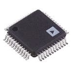
| 供应商器件封装 | 48-LQFP(7x7) |
| 分辨率 | 8 bit |
| 包装 | 托盘 |
| 商标 | Analog Devices |
| 安装类型 | 表面贴装 |
| 安装风格 | SMD/SMT |
| 封装 | Tray |
| 封装/外壳 | 48-LQFP |
| 封装/箱体 | LQFP-48 |
| 工作温度 | -40°C ~ 85°C |
| 工作电源电压 | 3.135 V to 5.25 V |
| 工厂包装数量 | 250 |
| 建立时间 | - |
| 数据接口 | 并联 |
| 最大功率耗散 | 485 mW |
| 最大工作温度 | + 85 C |
| 最小工作温度 | - 40 C |
| 标准包装 | 1 |
| 电压源 | 单电源 |
| 类型 | Video Encoder |
| 系列 | ADV7125 |
| 转换器数 | 3 |
| 输出数和类型 | 6 电流,单极 |
| 通道数量 | 3 Channel |
| 采样率(每秒) | 50M |


- 商务部:美国ITC正式对集成电路等产品启动337调查
- 曝三星4nm工艺存在良率问题 高通将骁龙8 Gen1或转产台积电
- 太阳诱电将投资9.5亿元在常州建新厂生产MLCC 预计2023年完工
- 英特尔发布欧洲新工厂建设计划 深化IDM 2.0 战略
- 台积电先进制程称霸业界 有大客户加持明年业绩稳了
- 达到5530亿美元!SIA预计今年全球半导体销售额将创下新高
- 英特尔拟将自动驾驶子公司Mobileye上市 估值或超500亿美元
- 三星加码芯片和SET,合并消费电子和移动部门,撤换高东真等 CEO
- 三星电子宣布重大人事变动 还合并消费电子和移动部门
- 海关总署:前11个月进口集成电路产品价值2.52万亿元 增长14.8%


PDF Datasheet 数据手册内容提取
CMOS, 330 MHz Triple 8-Bit High Speed Video DAC Data Sheet ADV7125 FEATURES FUNCTIONAL BLOCK DIAGRAM 330 MSPS throughput rate VAA Triple 8-bit DACs RS-343A-/RS-170-compatible output BLANK BLANKAND Complementary outputs SYNC SYNC LOGIC DAC output current range: 2.0 mA to 26.5 mA DATA IOR TTL-compatible inputs R7TO R0 8 REGISTER 8 DAC IOR Internal reference (1.235 V) DATA IOG Single-supply +5 V/+3.3 V operation G7TO G0 8 REGISTER 8 DAC IOG 48-lead LQFP and LFCSP Low power dissipation (30 mW minimum at 3 V) DATA IOB B7TO B0 8 REGISTER 8 DAC Low power standby mode (6 mW typical at 3 V) IOB Industrial temperature range (−40°C to +85°C) POWER-DOWN VOLTAGE RoHS compliant packages PSAVE MODE REFERENCE VREF CIRCUIT Qualified for automotive applications CLOCK APPLICATIONS GND RSET COMP ADV7125 03097-001 Digital video systems Figure 1. High resolution color graphics Digital radio modulation Image processing Instrumentation Video signal reconstruction Automotive infotainment units GENERAL DESCRIPTION The ADV7125 (ADV®) is a triple high speed, digital-to-analog The ADV7125 is fabricated in a 5 V CMOS process. Its converter (DAC) on a single monolithic chip. It consists of three monolithic CMOS construction ensures greater functionality high speed, 8-bit video DACs with complementary outputs, a with lower power dissipation. The ADV7125 is available in 48- standard TTL input interface, and a high impedance, analog lead LQFP and 48-lead LFCSP packages. output current source. PRODUCT HIGHLIGHTS The ADV7125 has three separate 8-bit-wide input ports. A 1. 330 MSPS (3.3 V only) throughput. single +5 V/+3.3 V power supply and clock are all that are 2. Guaranteed monotonic to eight bits. required to make the device functional. The ADV7125 has 3. Compatible with a wide variety of high resolution color additional video control signals, composite SYNC and BLANK, graphics systems, including RS-343A and RS-170. as well as a power save mode. Rev. D Document Feedback Information furnished by Analog Devices is believed to be accurate and reliable. However, no responsibility is assumed by Analog Devices for its use, nor for any infringements of patents or other One Technology Way, P.O. Box 9106, Norwood, MA 02062-9106, U.S.A. rights of third parties that may result from its use. Specifications subject to change without notice. No license is granted by implication or otherwise under any patent or patent rights of Analog Devices. Tel: 781.329.4700 ©2002–2016 Analog Devices, Inc. All rights reserved. Trademarks and registered trademarks are the property of their respective owners. Technical Support www.analog.com
ADV7125 Data Sheet TABLE OF CONTENTS Features .............................................................................................. 1 Circuit Description and Operation .............................................. 12 Applications ....................................................................................... 1 Digital Inputs .............................................................................. 12 Functional Block Diagram .............................................................. 1 Clock Input .................................................................................. 12 General Description ......................................................................... 1 Video Synchronization and Control ........................................ 13 Product Highlights ........................................................................... 1 Reference Input ........................................................................... 13 Revision History ............................................................................... 2 DACs ............................................................................................ 13 Specifications ..................................................................................... 3 Analog Outputs .......................................................................... 13 5 V Electrical Characteristics ...................................................... 3 Gray Scale Operation ................................................................. 14 3.3 V Electrical Characteristics ................................................... 4 Video Output Buffers ................................................................. 14 5 V Timing Specifications ........................................................... 5 PCB Layout Considerations ...................................................... 14 3.3 V Timing Specifications ........................................................ 6 Digital Signal Interconnect ....................................................... 14 Absolute Maximum Ratings ............................................................ 7 Analog Signal Interconnect....................................................... 15 ESD Caution .................................................................................. 7 Outline Dimensions ....................................................................... 16 Pin Configurations and Function Descriptions ........................... 8 Ordering Guide .......................................................................... 17 Terminology .................................................................................... 11 Automotive Products ................................................................. 17 REVISION HISTORY 4/16—Rev. C to Rev. D 3/09—Rev. 0 to Rev. A Changes to Figure 3 and Table 6 ..................................................... 8 Updated Format .................................................................. Universal Added Figure 4; Renumbered Sequentially .................................. 8 Changes to Features Section, Applications Section, and Added Figure 5 and Table 7; Renumbered Sequentially ........... 10 General Description Section ............................................................ 1 Updated Outline Dimensions ....................................................... 16 Changes to Figure 3 and Table 6 ...................................................... 8 Changes to Ordering Guide .......................................................... 17 Deleted Ground Planes Section, Power Planes Section, and Supply Decoupling Section ........................................................... 11 2/11—Rev. B to Rev. C Changes to Figure 5 ........................................................................ 11 Change to Table 6 ............................................................................. 8 Changes to Table 7, Analog Outputs Section, Figure 6, and Figure 7 ............................................................................................ 12 7/10—Rev. A to Rev. B Changes to Video Output Buffers Section, PCB Layout Change to Features Section ............................................................. 1 Considerations Section, and Figure 9 .......................................... 13 Changes to Clock Frequency Parameter, Table 4 ......................... 6 Changes to Analog Signal Interconnect Section and Figure 10 .... 14 Changes to Figure 2 .......................................................................... 6 Updated Outline Dimensions ....................................................... 15 Changes to Figure 4 and Figure 5 ................................................. 11 Changes to Ordering Guide .......................................................... 16 Changes to Table 7 .......................................................................... 12 Changes to Endnotes to Ordering Guide .................................... 15 10/02—Revision 0: Initial Version Added Automotive Products Section .......................................... 15 Rev. D | Page 2 of 17
Data Sheet ADV7125 SPECIFICATIONS 5 V ELECTRICAL CHARACTERISTICS V = 5 V ± 5%, V = 1.235 V, R = 560 Ω, C = 10 pF. All specifications T to T ,1 unless otherwise noted, T = 110°C. AA REF SET L MIN MAX J MAX Table 1. Parameter Min Typ Max Unit Test Conditions/Comments1 STATIC PERFORMANCE Resolution (Each DAC) 8 Bits Integral Nonlinearity (BSL) −1 ±0.4 +1 LSB Differential Nonlinearity −1 ±0.25 +1 LSB Guaranteed Monotonic DIGITAL AND CONTROL INPUTS Input High Voltage, V 2 V IH Input Low Voltage, V 0.8 V IL Input Current, I −1 +1 μA V = 0.0 V or V IN IN DD PSAVE Pull-Up Current 20 μA Input Capacitance, C 10 pF IN ANALOG OUTPUTS Output Current 2.0 26.5 mA Green DAC, SYNC = high 2.0 18.5 mA RGB DAC, SYNC = low DAC-to-DAC Matching 1.0 5 % Output Compliance Range, V 0 1.4 V OC Output Impedance, R 100 kΩ OUT Output Capacitance, C 10 pF I = 0 mA OUT OUT Offset Error −0.025 +0.025 % FSR Tested with DAC output = 0 V Gain Error2 −5.0 +5.0 % FSR FSR = 18.62 mA VOLTAGE REFERENCE, EXTERNAL AND INTERNAL Reference Range, V 1.12 1.235 1.35 V REF POWER DISSIPATION Digital Supply Current3 3.4 9 mA f = 50 MHz CLK 10.5 15 mA f = 140 MHz CLK 18 25 mA f = 240 MHz CLK Analog Supply Current 67 72 mA R = 530 Ω SET 8 mA R = 4933 Ω SET Standby Supply Current4 2.1 5.0 mA PSAVE = low, digital, and control inputs at V DD Power Supply Rejection Ratio 0.1 0.5 %/% 1 Temperature range TMIN to TMAX: −40°C to +85°C at 50 MHz and 140 MHz, 0°C to +70°C at 240 MHz and 330 MHz. 2 Gain error = ((Measured (FSC)/Ideal (FSC) − 1) × 100), where Ideal = VREF/RSET × K × (0xFFH) × 4 and K = 7.9896. 3 Digital supply is measured with a continuous clock that has data input corresponding to a ramp pattern and with an input level at 0 V and VDD. 4 These maximum/minimum specifications are guaranteed by characterization in the 4.75 V to 5.25 V range. Rev. D | Page 3 of 17
ADV7125 Data Sheet 3.3 V ELECTRICAL CHARACTERISTICS V = 3.0 V to 3.6 V, V = 1.235 V, R = 560 Ω, C = 10 pF. All specifications T to T ,1 unless otherwise noted, T = 110°C. AA REF SET L MIN MAX J MAX Table 2. Parameter2 Min Typ Max Unit Test Conditions/Comments1 STATIC PERFORMANCE Resolution (Each DAC) 8 Bits R = 680 Ω SET Integral Nonlinearity (BSL) −1 ±0.5 +1 LSB R = 680 Ω SET Differential Nonlinearity −1 ±0.25 +1 LSB R = 680 Ω SET DIGITAL AND CONTROL INPUTS Input High Voltage, V 2.0 V IH Input Low Voltage, V 0.8 V IL Input Current, I −1 +1 μA V = 0.0 V or V IN IN DD PSAVE Pull-Up Current 20 μA Input Capacitance, C 10 pF IN ANALOG OUTPUTS Output Current 2.0 26.5 mA Green DAC, SYNC = high 2.0 18.5 mA RGB DAC, SYNC = low DAC-to-DAC Matching 1.0 % Output Compliance Range, V 0 1.4 V OC Output Impedance, R 70 kΩ OUT Output Capacitance, C 10 pF OUT Offset Error 0 0 % FSR Tested with DAC output = 0 V Gain Error3 0 % FSR FSR = 18.62 mA VOLTAGE REFERENCE, EXTERNAL Reference Range, V 1.12 1.235 1.35 V REF VOLTAGE REFERENCE, INTERNAL Voltage Reference, V 1.235 V REF POWER DISSIPATION Digital Supply Current4 2.2 5.0 mA f = 50 MHz CLK 6.5 12.0 mA f = 140 MHz CLK 11 15 mA f = 240 MHz CLK 16 mA f = 330 MHz CLK Analog Supply Current 67 72 mA R = 560 Ω SET 8 mA R = 4933 Ω SET Standby Supply Current 2.1 5.0 mA PSAVE = low, digital, and control inputs at V DD Power Supply Rejection Ratio 0.1 0.5 %/% 1 Temperature range TMIN to TMAX: −40°C to +85°C at 50 MHz and 140 MHz, 0°C to +70°C at 240 MHz and 330 MHz. 2 These max/min specifications are guaranteed by characterization in the 3.0 V to 3.6 V range. 3 Gain error = ((Measured (FSC)/Ideal (FSC) −1) × 100), where Ideal = VREF/RSET × K × (0xFFH) × 4 and K = 7.9896. 4 Digital supply is measured with continuous clock that has data input corresponding to a ramp pattern and with an input level at 0 V and VDD. Rev. D | Page 4 of 17
Data Sheet ADV7125 5 V TIMING SPECIFICATIONS V = 5 V ± 5%,1 V = 1.235 V, R = 560 Ω, C = 10 pF. All specifications T to T ,2 unless otherwise noted, T = 110°C. AA REF SET L MIN MAX J MAX Table 3. Parameter3 Symbol Min Typ Max Unit Test Conditions/Comments ANALOG OUTPUTS Analog Output Delay t 5.5 ns 6 Analog Output Rise/Fall Time4 t 1.0 ns 7 Analog Output Transition Time5 t 15 ns 8 Analog Output Skew6 t 1 2 ns 9 CLOCK CONTROL CLOCK Frequency7 f 0.5 50 MHz 50 MHz grade CLK 0.5 140 MHz 140 MHz grade 0.5 240 MHz 240 MHz grade Data and Control Setup6 t 0.5 ns 1 Data and Control Hold6 t 1.5 ns 2 CLOCK Period t 4.17 ns 3 CLOCK Pulse Width High6 t 1.875 ns f = 240 MHz 4 CLK_MAX CLOCK Pulse Width Low6 t 1.875 ns f = 240 MHz 5 CLK_MAX CLOCK Pulse Width High6 t 2.85 ns f = 140 MHz 4 CLK_MAX CLOCK Pulse Width Low6 t 2.85 ns f = 140 MHz 5 CLK_MAX CLOCK Pulse Width High t 8.0 ns f = 50 MHz 4 CLK_MAX CLOCK Pulse Width Low t 8.0 ns f = 50 MHz 5 CLK_MAX Pipeline Delay6 t 1.0 1.0 1.0 Clock cycles PD PSAVE Up Time6 t10 2 10 ns 1 The maximum and minimum specifications are guaranteed over this range. 2 Temperature range TMIN to TMAX: −40°C to +85°C at 50 MHz and 140 MHz, 0°C to +70°C at 240 MHz. 3 Timing specifications are measured with input levels of 3.0 V (VIH) and 0 V (VIL) for both 5 V and 3.3 V supplies. 4 Rise time was measured from the 10% to 90% point of zero to full-scale transition, fall time from the 90% to 10% point of a full-scale transition. 5 Measured from 50% point of full-scale transition to 2% of final value. 6 Guaranteed by characterization. 7 fCLK maximum specification production tested at 125 MHz and 5 V. Limits specified here are guaranteed by characterization. Rev. D | Page 5 of 17
ADV7125 Data Sheet 3.3 V TIMING SPECIFICATIONS V = 3.0 V to 3.6 V,1 V = 1.235 V, R = 560 Ω, C = 10 pF. All specifications T to T ,2 unless otherwise noted, T = 110°C. AA REF SET L MIN MAX J MAX Table 4. Parameter3 Symbol Min Typ Max Unit Test Conditions/Comments ANALOG OUTPUTS Analog Output Delay, t 7.5 ns 6 Analog Output Rise/Fall Time4 t 1.0 ns 7 Analog Output Transition Time5 t 15 ns 8 Analog Output Skew6 t 1 2 ns 9 CLOCK CONTROL CLOCK Frequency7 f 50 MHz 50 MHz grade CLK 140 MHz 140 MHz grade 240 MHz 240 MHz grade 330 MHz 330 MHz grade Data and Control Setup6 t 0.2 ns 1 Data and Control Hold6 t 1.5 ns 2 CLOCK Period t 3 ns 3 CLOCK Pulse Width High6 t 1.4 ns f = 330 MHz 4 CLK_MAX CLOCK Pulse Width Low6 t 1.4 ns f = 330 MHz 5 CLK_MAX CLOCK Pulse Width High6 t 1.875 ns f = 240 MHz 4 CLK_MAX CLOCK Pulse Width Low6 t 1.875 ns f = 240 MHz 5 CLK_MAX CLOCK Pulse Width High6 t 2.85 ns f = 140 MHz 4 CLK_MAX CLOCK Pulse Width Low6 t 2.85 ns f = 140 MHz 5 CLK_MAX CLOCK Pulse Width High t 8.0 ns f = 50 MHz 4 CLK_MAX CLOCK Pulse Width Low t 8.0 ns f = 50 MHz 5 CLK_MAX Pipeline Delay6 t 1.0 1.0 1.0 Clock cycles PD PSAVE Up Time6 t10 4 10 ns 1 These maximum and minimum specifications are guaranteed over this range. 2 Temperature range: TMIN to TMAX: −40°C to +85°C at 50 MHz and 140 MHz, 0°C to +70°C at 240 MHz and 330 MHz. 3 Timing specifications are measured with input levels of 3.0 V (VIH) and 0 V (VIL) for 3.3 V supplies. 4 Rise time was measured from the 10% to 90% point of zero to full-scale transition, fall time from the 90% to 10% point of a full-scale transition. 5 Measured from 50% point of full-scale transition to 2% of final value. 6 Guaranteed by characterization. 7 fCLK maximum specification production tested at 125 MHz and 5 V. Limits specified here are guaranteed by characterization. t3 t4 t5 CLOCK t2 DIGITAL INPUTS (R7 TO R0, G7 TO G0, B7 TO B0, SYNC, BLANK) t1 t6 t8 ANALOG OUTPUTS (IOR, IOR, IOG, IOG, IOB, IOB) t7 NOTES 1. OUTPUT DELAY (t6) MEASURED FROM THE 50% POINT OF THE RISING EDGE OF CLOCK TO THE 50% POINT OF FULL-SCALE TRANSITION. 32 .. TOFRIUNATANPLSU OITTU IROTINSPEU T/TIFM AVELA LL(t U8T)EI MM.EE A(tS7)U MREEADS FURROEMD TBHEET W50E%E NP OTIHNET 1O0F% F AUNLDL -9S0C%A LPEO ITNRTASN OSFIT FIOUNL LT-OSC WAILTEH ITNR 2A%N SOIFT ITOHNE. 03097-002 Figure 2. Timing Diagram Rev. D | Page 6 of 17
Data Sheet ADV7125 ABSOLUTE MAXIMUM RATINGS Stresses at or above those listed under Absolute Maximum Table 5. Ratings may cause permanent damage to the product. This is a Parameter Rating stress rating only; functional operation of the product at these V to GND 7 V AA or any other conditions above those indicated in the operational Voltage on Any Digital Pin GND − 0.5 V to V + 0.5 V AA section of this specification is not implied. Operation beyond Ambient Operating Temperature −40°C to +85°C the maximum operating conditions for extended periods may Range (T ) A affect product reliability. Storage Temperature Range (T) −65°C to +150°C S Junction Temperature (T) 150°C J Lead Temperature (Soldering, 10 sec) 300°C ESD CAUTION Vapor Phase Soldering (1 Minute) 220°C I to GND1 0 V to V OUT AA 1 Analog output short circuit to any power supply or common GND can be of an indefinite duration. Rev. D | Page 7 of 17
ADV7125 Data Sheet PIN CONFIGURATIONS AND FUNCTION DESCRIPTIONS E R7R6R5R4R3R2R1R0GNDGNDPSAVRSET 876543210987 444444444333 E GND 1 PIN 1 36VREF R7R6R5R4R3R2R1R0GNDGNDPSAVRSET GND 2 INDICATOR 35COMP 847464544434241404938373 G0 3 34IOR G1 4 33IOR G2 5 32IOG GND 1 36 VREF GND 2 35 COMP G3 6 ADV7125 31IOG G0 3 34 IOR G4 7 TOP VIEW 30VAA G1 4 33 IOR G5 8 (Not to Scale) 29VAA GG23 56 ATDOPV V7I1E2W5 3312 IIOOGG G6 9 28IOB G4 7 (Not to Scale) 30 VAA G7 10 27IOB G5 8 29 VAA BLANK 11 26GND G6 9 28 IOB G7 10 27 IOB SYNC 12 25GND BLANK 11 26 GND SYNC 12 25 GND 131415161718192021222324 314151617181910212223242 VAAGNDGNDB0B1B2B3B4B5B6B7CLOCK VAAGNDGNDB0B1B2B3B4B5B6B7CLOCK N1.O TTHEES EXPOSED PADDLE MUST BE CONNECTED TO GND. 03097-003 N1.O TTHEES EXPOSEDPADDLE MUST BE CONNECTEDTO GND. 03097-100 Figure 3. LFCSP Pin Configuration (CP-48-1) Figure 4. LFCSP Pin Configuration (CP-48-4) Table 6. LFCSP Pin Function Descriptions Pin No. Mnemonic Description 1, 2, 14, 15, GND Ground. All GND pins must be connected. 25, 26, 39, 40 3 to 10, 16 to G0 to G7, Red, Green, and Blue Pixel Data Inputs (TTL Compatible). Pixel data is latched on the rising edge of CLOCK. 23, 41 to 48 B0 to B7, R0, G0, and B0 are the least significant data bits. Unused pixel data inputs should be connected to either the R0 to R7 regular printed circuit board (PCB) power or ground plane. 11 BLANK Composite Blank Control Input (TTL Compatible). A Logic 0 on this control input drives the analog outputs, IOR, IOB, and IOG, to the blanking level. The BLANK signal is latched on the rising edge of CLOCK. While BLANK is a Logic 0, the R0 to R7, G0 to G7, and B0 to B7 pixel inputs are ignored. 12 SYNC Composite Sync Control Input (TTL Compatible). A Logic 0 on the SYNC input switches off a 40 IRE current source. This is internally connected to the IOG analog output. SYNC does not override any other control or data input; therefore, it should only be asserted during the blanking interval. SYNC is latched on the rising edge of CLOCK. If sync information is not required on the green channel, the SYNC input should be tied to Logic 0. 13, 29, 30 V Analog Power Supply (5 V ± 5%). All V pins on the ADV7125 must be connected. AA AA 24 CLOCK Clock Input (TTL Compatible). The rising edge of CLOCK latches the R0 to R7, G0 to G7, B0 to B7, SYNC, and BLANK pixel and control inputs. It is typically the pixel clock rate of the video system. CLOCK should be driven by a dedicated TTL buffer. 27, 31, 33 IOB, IOG, Differential Blue, Green, and Red Current Outputs (High Impedance Current Sources). These RGB video IOR outputs are specified to directly drive RS-343A and RS-170 video levels into a doubly terminated 75 Ω load. If the complementary outputs are not required, these outputs should be tied to ground. 28, 32, 34 IOB, IOG, Blue, Green, and Red Current Outputs. These high impedance current sources are capable of directly driving IOR a doubly terminated 75 Ω coaxial cable. All three current outputs should have similar output loads whether or not they are all being used. 35 COMP Compensation Pin. This is a compensation pin for the internal reference amplifier. A 0.1 μF ceramic capacitor must be connected between COMP and V . AA 36 V Voltage Reference Input for DACs or Voltage Reference Output (1.235 V). REF Rev. D | Page 8 of 17
Data Sheet ADV7125 Pin No. Mnemonic Description 37 R A resistor (R ) connected between this pin and GND controls the magnitude of the full-scale video signal. SET SET Note that the IRE relationships are maintained, regardless of the full-scale output current. The relationship between R and the full-scale output current on IOG (assuming I is connected to IOG) is given by: SET SYNC R (Ω) = 11,445 × V (V)/IOG (mA) SET REF The relationship between R and the full-scale output current on IOR, IOG, and IOB is given by: SET IOG (mA) = 11,444.8 × V (V)/R (Ω) (SYNC being asserted) REF SET IOR, IOB (mA) = 7989.6 × V (V)/R (Ω) REF SET The equation for IOG is the same as that for IOR and IOB when SYNC is not being used, that is, SYNC tied permanently low. 38 PSAVE Power Save Control Pin. Reduced power consumption is available on the ADV7125 when this pin is active. 0 EPAD Exposed Paddle. The exposed paddle must be connected to GND. Rev. D | Page 9 of 17
ADV7125 Data Sheet E R7 R6 R5 R4 R3 R2 R1 R0 GND GND PSAV RSET 48 47 46 45 44 43 42 41 40 39 38 37 GND 1 36 VREF GND 2 35 COMP G0 3 34 IOR G1 4 33 IOR G2 5 ADV7125 32 IOG G3 6 TOP VIEW 31 IOG (Not to Scale) G4 7 30 VAA G5 8 29 VAA G6 9 28 IOB G7 10 27 IOB BLANK 11 26 GND SYNC 12 25 GND 13 14 15 16 17 18 19 20 21 22 23 24 VAAGND GND B0 B1 B2 B3 B4 B5 B6 B7 CLOCK 03907-101 Figure 5. LQFP Pin Configuration Table 7. LQFP Pin Function Descriptions Pin No. Mnemonic Description 1, 2, 14, 15, GND Ground. All GND pins must be connected. 25, 26, 39, 40 3 to 10, 16 to G0 to G7, Red, Green, and Blue Pixel Data Inputs (TTL Compatible). Pixel data is latched on the rising edge of CLOCK. R0, 23, 41 to 48 B0 to B7, G0, and B0 are the least significant data bits. Unused pixel data inputs should be connected to either the R0 to R7 regular printed circuit board (PCB) power or ground plane. 11 BLANK Composite Blank Control Input (TTL Compatible). A Logic 0 on this control input drives the analog outputs, IOR, IOB, and IOG, to the blanking level. The BLANK signal is latched on the rising edge of CLOCK. While BLANK is a Logic 0, the R0 to R7, G0 to G7, and B0 to B7 pixel inputs are ignored. 12 SYNC Composite Sync Control Input (TTL Compatible). A Logic 0 on the SYNC input switches off a 40 IRE current source. This is internally connected to the IOG analog output. SYNC does not override any other control or data input; therefore, it should only be asserted during the blanking interval. SYNC is latched on the rising edge of CLOCK. If sync information is not required on the green channel, the SYNC input should be tied to Logic 0. 13, 29, 30 V Analog Power Supply (5 V ± 5%). All V pins on the ADV7125 must be connected. AA AA 24 CLOCK Clock Input (TTL Compatible). The rising edge of CLOCK latches the R0 to R7, G0 to G7, B0 to B7, SYNC, and BLANK pixel and control inputs. It is typically the pixel clock rate of the video system. CLOCK should be driven by a dedicated TTL buffer. 27, 31, 33 IOB, IOG, Differential Blue, Green, and Red Current Outputs (High Impedance Current Sources). These RGB video IOR outputs are specified to directly drive RS-343A and RS-170 video levels into a doubly terminated 75 Ω load. If the complementary outputs are not required, these outputs should be tied to ground. 28, 32, 34 IOB, IOG, Blue, Green, and Red Current Outputs. These high impedance current sources are capable of directly driving a IOR doubly terminated 75 Ω coaxial cable. All three current outputs should have similar output loads whether or not they are all being used. 35 COMP Compensation Pin. This is a compensation pin for the internal reference amplifier. A 0.1 μF ceramic capacitor must be connected between COMP and V . AA 36 V Voltage Reference Input for DACs or Voltage Reference Output (1.235 V). REF 37 R A resistor (R ) connected between this pin and GND controls the magnitude of the full-scale video signal. SET SET Note that the IRE relationships are maintained, regardless of the full-scale output current. The relationship between R and the full-scale output current on IOG (assuming I is connected to IOG) is given by: SET SYNC R (Ω) = 11,445 × V (V)/IOG (mA) SET REF The relationship between R and the full-scale output current on IOR, IOG, and IOB is given by: SET IOG (mA) = 11,444.8 × V (V)/R (Ω) (SYNC being asserted) REF SET IOR, IOB (mA) = 7989.6 × V (V)/R (Ω) REF SET The equation for IOG is the same as that for IOR and IOB when SYNC is not being used, that is, SYNC tied permanently low. 38 PSAVE Power Save Control Pin. Reduced power consumption is available on the ADV7125 when this pin is active. Rev. D | Page 10 of 17
Data Sheet ADV7125 TERMINOLOGY Raster Scan Blanking Level The most basic method of sweeping a CRT one line at a time to The level separating the SYNC portion from the video portion generate and display images. of the waveform. Usually referred to as the front porch or back porch. At 0 IRE units, it is the level that shuts off the picture Reference Black Level tube, resulting in the blackest possible picture. The maximum negative polarity amplitude of the video signal. Color Video (RGB) Reference White Level This refers to the technique of combining the three primary The maximum positive polarity amplitude of the video signal. colors of red, green, and blue to produce color pictures within Sync Level the usual spectrum. In RGB monitors, three DACs are required, The peak level of the SYNC signal. one for each color. Video Signal Sync Signal (SYNC) The portion of the composite video signal that varies in gray The position of the composite video signal that synchronizes scale levels between reference white and reference black. Also the scanning process. referred to as the picture signal, this is the portion that can be Gray Scale visually observed. The discrete levels of video signal between reference black and reference white levels. An 8-bit DAC contains 256 different levels. Rev. D | Page 11 of 17
ADV7125 Data Sheet CIRCUIT DESCRIPTION AND OPERATION The ADV7125 contains three 8-bit DACs, with three input Table 8 details the resultant effect on the analog outputs of channels, each containing an 8-bit register. Also integrated BLANK and SYNC. on board the device is a reference amplifier. The CRT control All these digital inputs are specified to accept TTL logic levels. functions, BLANK and SYNC, are integrated on board the CLOCK INPUT ADV7125. DIGITAL INPUTS The CLOCK input of the ADV7125 is typically the pixel clock rate of the system. It is also known as the dot rate. The dot rate, There are 24 bits of pixel data (color information), R0 to R7, and thus the required CLOCK frequency, is determined by the G0 to G7, and B0 to B7, latched into the device on the rising on-screen resolution, according to the following equation: edge of each clock cycle. This data is presented to the three 8-bit Dot Rate = (Horiz Res) × (Vert Res) × (Refresh DACs and then converted to three analog (RGB) output wave- Rate)/(Retrace Factor) forms (see Figure 6). where: CLOCK Horiz Res is the number of pixels per line. DIGITAL INPUTS (R7 TO R0, G7 TO G0, Vert Res is the number of lines per frame. DATA B7 TO B0, Refresh Rate is the horizontal scan rate. This is the rate at which SYNC, BLANK) the screen must be refreshed, typically 60 Hz for a noninterlaced (AIONRA,L IOOGR ,O IIOOUBGT,P, IUIOOTBGS), 03097-004 sRyesttreamce, Foar c3t0or H isz tfhoer taont ainl btelarlnakc etdim syes ftaecmto. r. This takes into Figure 6. Video Data Input/Output account that the display is blanked for a certain fraction of the total duration of each frame (for example, 0.8). The ADV7125 has two additional control signals that are latched to the analog video outputs in a similar fashion. BLANK and Therefore, for a graphics system with a 1024 × 1024 resolution, SYNC are each latched on the rising edge of CLOCK to maintain a noninterlaced 60 Hz refresh rate, and a retrace factor of 0.8, synchronization with the pixel data stream. Dot Rate = 1024 × 1024 × 60/0.8 = 78.6 MHz The BLANK and SYNC functions allow for the encoding of The required CLOCK frequency is thus 78.6 MHz. All video these video synchronization signals onto the RGB video output. data and control inputs are latched into the ADV7125 on the This is done by adding appropriately weighted current sources rising edge of CLOCK, as previously described in the Digital to the analog outputs, as determined by the logic levels on the Inputs section. It is recommended that the CLOCK input to the BLANK and SYNC digital inputs. ADV7125 be driven by a TTL buffer (for example, the 74F244). Figure 7 shows the analog output, RGB video waveform of the ADV7125. The influence of SYNC and BLANK on the analog video waveform is illustrated. RED AND BLUE GREEN mA V mA V 18.67 0.7 26.0 0.975 WHITE LEVEL 0 0 7.2 0.271 BLANK LEVEL 0 0 SYNC LEVEL NOTES 123... OVRRSUE-T3FP4 =U3 1TL.SE2 3VC5EOVLN,S RN ASEENCTDT = ET D5O3 LT0EOΩR. AA NDCOEUSB LAYS STUEMRMEDIN OATNE ADL 7L5 LΩE LVOEALSD.. 03097-005 Figure 7. Typical RGB Video Output Waveform Rev. D | Page 12 of 17
Data Sheet ADV7125 Table 8. Typical Video Output Truth Table (R = 530 Ω, R = 37.5 Ω) SET LOAD Video Output Level IOG (mA) IOG (mA) IOR/IOB (mA) IOR/IOB (mA) SYNC BLANK DAC Input Data White Level 26.0 0 18.67 0 1 1 0xFFH Video Video + 7.2 18.67 − Video Video 18.67 − Video 1 1 Data Video to BLANK Video 18.67 − Video Video 18.67 − Video 0 1 Data Black Level 7.2 18.67 0 18.67 1 1 0x00H Black to BLANK 0 18.67 0 18.67 0 1 0x00H BLANK Level 7.2 18.67 0 18.67 1 0 0xXXH (don’t care) SYNC Level 0 18.67 0 18.67 0 0 0xXXH (don’t care) VIDEO SYNCHRONIZATION AND CONTROL full-scale output current against temperature and power supply variations. The ADV7125 has a single composite sync (SYNC) input control. Many graphics processors and CRT controllers have the ANALOG OUTPUTS ability to generate horizontal sync (HSYNC), vertical sync The ADV7125 has three analog outputs, corresponding to the (VSYNC), and composite SYNC. red, green, and blue video signals. In a graphics system that does not automatically generate a The red, green, and blue analog outputs of the ADV7125 are composite SYNC signal, the inclusion of some additional logic high impedance current sources. Each one of these three RGB circuitry enables the generation of a composite SYNC signal. current outputs is capable of directly driving a 37.5 Ω load, such as a doubly terminated 75 Ω coaxial cable. Figure 8 shows the The sync current is internally connected directly to the IOG required configuration for each of the three RGB outputs output, thus encoding video synchronization information onto connected into a doubly terminated 75 Ω load. This arrangement the green video channel. If it is not required to encode sync develops RS-343A video output voltage levels across a 75 Ω information onto the ADV7125, the SYNC input should be tied monitor. to logic low. A suggested method of driving RS-170 video levels into a 75 Ω REFERENCE INPUT monitor is shown in Figure 9. The output current levels of the The ADV7125 contains an on-board voltage reference. The VREF DACs remain unchanged, but the source termination resistance, pin should be connected as shown in Figure 12. Z, on each of the three DACs is increased from 75 Ω to 150 Ω. S A resistance, RSET, connected between the RSET pin and GND, IOR, IOG, IOB Z0 = 75Ω determines the amplitude of the output video level according to DACs Equation 1 and Equation 2 for the ADV7125. (CABLE) IOG (mA) = 11,444.8 × VREF (V)/RSET (Ω) (1) TERM(ISZNOSA U=T RI7OC5NΩE) Z(ML O=N 7I5TΩOR) IOR, IOB (mA) = 7989.6 × V (V)/R (Ω) (2) REF SET Equation 1 applies to the ADV7125 only, when SYNC is being TEFROMRIN RAETDIO, NG RREEEPNE,AATNEDD BTLHUREE ED ATCIMsES 03097-006 used. If SYNC is not being encoded onto the green channel, Figure 8. Analog Output Termination for RS-343A Equation 1 is similar to Equation 2. IOR, IOG, IOB Using a variable value of R allows for accurate adjustment of Z0 = 75Ω SET DACs the analog output video levels. Use of a fixed 560 Ω R resistor SET (CABLE) yields the analog output levels quoted in the Specifications section. Z(SSO =U 1R5C0ΩE ZL = 75Ω (MONITOR) These values typically correspond to the RS-343A video wave- TERMINATION) form values, as shown in Figure 7. DACs TEFROMRIN RAETDIO, NG RREEEPNE,AATNEDD BTLHUREE ED ATCIMsES 03097-007 The ADV7125 contains three matched 8-bit DACs. The DACs Figure 9. Analog Output Termination for RS-170 are designed using an advanced, high speed, segmented architec- More detailed information regarding load terminations for ture. The bit currents corresponding to each digital input are various output configurations, including RS-343A and RS-170, routed to either the analog output (bit = 1) or GND (bit = 0) is available in the AN-205 Application Note, Video Formats and by a sophisticated decoding scheme. Because all this circuitry Required Load Terminations. is on one monolithic device, matching between the three DACs is optimized. As well as matching, the use of identical current Figure 7 shows the video waveforms associated with the three sources in a monolithic design guarantees monotonicity and RGB outputs driving the doubly terminated 75 Ω load of low glitch. The on-board operational amplifier stabilizes the Figure 8. As well as the gray scale levels (black level to white Rev. D | Page 13 of 17
ADV7125 Data Sheet level), Figure 7 also shows the contributions of SYNC and Z2 Z1 BLANK for the ADV7125. These control inputs add appro- +VS 0.1µF priately weighted currents to the analog outputs, producing 4 the specific output level requirements for video applications. IOR, IOG, IOB 2 75Ω Z0 = 75Ω AD848 7 Table 8 details how the SYNC and BLANK inputs modify the DACs 3 6 0.1µF (CABLE) ZL = 75Ω output levels. (MONITOR) GThReA AYD SVC71A2L5 Ec aOn PbEe RusAedT IfOorN st andalone, gray scale (mono- TERM(ISZNOSA UT= RI7OC5NΩE) –VS GAIN (G) = 1 +ZZ12 03097-009 Figure 11. AD848 as an Output Buffer chrome) or composite video applications (that is, only one channel used for video information). Any one of the three channels, red, PCB LAYOUT CONSIDERATIONS green, or blue, can be used to input the digital video data. The The ADV7125 is optimally designed for lowest noise perfor- two unused video data channels should be tied to Logic 0. The mance, both radiated and conducted noise. To complement the unused analog outputs should be terminated with the same load excellent noise performance of the ADV7125, it is imperative as that for the used channel, that is, if the red channel is used that great care be given to the PCB layout. Figure 12 shows a and IOR is terminated with a doubly terminated 75 Ω load recommended connection diagram for the ADV7125. (37.5 Ω), IOB and IOG should be terminated with 37.5 Ω The layout should be optimized for lowest noise on the resistors (see Figure 10). ADV7125 power and ground lines. This can be achieved by DOUBLY OUVTIDPEUOT RR07 IIOOGR T75EΩR MLOINAADTED sShhioerldteinn gt hthe ele daidg ilteanl ginthp ubtest waneden p grorovuidpisn go fg VooAAd adnedc oGuNplDin pg.i n s ADV7125 37.5Ω to minimize inductive ringing. G0 G7 IOB It is recommended to use a 4-layer printed circuit board with a 37.5Ω single ground plane. The ground and power planes should B0 B7 GND 03097-008 soenp tahrea taen tahleo gsi gpnoawle trr apclea nlaey cearn a nbde ftuhret hsoelrd reerd suidceed l abyye ru. sNinogis e Figure 10. Input and Output Connections for Standalone Gray Scale or multiple decoupling capacitors (see Figure 12). Optimum Composite Video performance is achieved by using 0.1 μF and 0.01 μF ceramic VIDEO OUTPUT BUFFERS capacitors. Individually decouple each VAA pin to ground by placing the capacitors as close as possible to the device with the The ADV7125 is specified to drive transmission line loads. The capacitor leads as short as possible, thus minimizing lead analog output configuration to drive such loads is described in the inductance. It is important to note that while the ADV7125 Analog Outputs section and illustrated in Figure 11. However, contains circuitry to reject power supply noise, this rejection in some applications, it may be required to drive long transmis- decreases with frequency. If a high frequency switching power sion line cable lengths. Cable lengths greater than 10 meters can supply is used, pay close attention to reducing power supply attenuate and distort high frequency analog output pulses. The noise. A dc power supply filter (Murata BNX002) provides EMI inclusion of output buffers compensates for some cable distortion. suppression between the switching power supply and the main Buffers with large full power bandwidths and gains between PCB. Alternatively, consideration can be given to using a 3- two and four are required. These buffers also need to be able terminal voltage regulator. to supply sufficient current over the complete output voltage swing. Analog Devices produces a range of suitable op amps for DIGITAL SIGNAL INTERCONNECT such applications. These include the AD843, AD844, AD847, Isolate the digital signal lines to the ADV7125 as much as and AD848 series of monolithic op amps. In very high frequency possible from the analog outputs and other analog circuitry. applications (80 MHz), the AD8061 is recommended. More Digital signal lines should not overlay the analog power plane. information on line driver buffering circuits is given in the Due to the high clock rates used, long clock lines to the relevant op amp data sheets. ADV7125 should be avoided to minimize noise pickup. Use of buffer amplifiers also allows implementation of other Connect any active pull-up termination resistors for the digital video standards besides RS-343A and RS-170. Altering the gain inputs to the regular PCB power plane (V ) and not to the components of the buffer circuit results in any desired video level. CC analog power plane. Rev. D | Page 14 of 17
Data Sheet ADV7125 ANALOG SIGNAL INTERCONNECT For optimum performance, the analog outputs should each have a source termination resistance to ground of 75 Ω (doubly Place the ADV7125 as close as possible to the output connectors, terminated 75 Ω configuration). This termination resistance thus minimizing noise pickup and reflections due to impedance should be as close as possible to the ADV7125 to minimize mismatch. reflections. The video output signals should overlay the ground plane and Additional information on PCB design is available in the not the analog power plane, thereby maximizing the high AN-333 Application Note, Design and Layout of a Video frequency power supply rejection. Graphics System for Reduced EMI. POWER SUPPLY DECOUPLING (0.1µFAND 0.01µF CAPACITOR FOR EACHVAAGROUP) 0.1µF 0.01µF 13, 29, 0.1µF 30 VAA 35 COMP VAA VAA 41TO 48 VAA 1kΩ R7TO R0 VREF 36 1 AD1580 1µF 2 3TO 10 RSET 37 VIDEO RSET DATA G7TO G0 530Ω COAXIAL CABLE MONITOR (CRT) INPUTS 75Ω IOR 34 16TO 23 75Ω B7TO B0 IOG 32 ADV7125 75Ω IOB 28 75Ω 75Ω 75Ω 75Ω BNC 12 SYNC IOR 33 CONNECTORS 11 BLANK IOG 31 COMPLEMENTARY 24 CLOCK OUTPUTS 38 PSAVE IOB 27 GND 21,5 ,2 ,2 61,4 ,3 91,5 ,40 03097-010 Figure 12. Typical Connection Diagram Rev. D | Page 15 of 17
ADV7125 Data Sheet OUTLINE DIMENSIONS 9.20 0.75 9.00 SQ 1.60 0.60 MAX 8.80 0.45 48 37 1 36 PIN 1 7.20 1.45 TOP VIEW 7.00 SQ 1.40 0.20 (PINS DOWN) 6.80 0.09 1.35 7° 00..1055 SPELAANTEING 0C.O08PL3A0.5°N°ARITY VIEW A 102.5103 240.2257 BSC 0.22 LEAD PITCH 0.17 VIEW A ROTATED 90° CCW COMPLIANTTO JEDEC STANDARDS MS-026-BBC 051706-A Figure 13. 48-Lead Low Profile Quad Flat Package [LQFP] (ST-48) Dimensions shown in millimeters 7.10 0.30 7.00 SQ 0.60 MAX 0.23 6.90 0.60 MAX 0.18 PIN 1 37 48 INDICATOR 36 1 PIN 1 INDICATOR 0.50 66..8755 SQ REF EXPOSED 5.25 6.65 PAD 5.10 SQ 4.95 25 12 0.50 24 13 0.25 MIN TOP VIEW 0.40 5.50 REF 0.30 12° MAX 0.80 MAX 1.00 0.85 0.65 TYP FOR PROPER CONNECTION OF 0.80 0.05 MAX TTHHEE PEIXNP COOSNEDFI GPAUDR,A RTEIOFNE RA NTOD 0.02 NOM FUNCTION DESCRIPTIONS SEATING COPL0A.0N8ARITY SECTION OF THIS DATA SHEET. PLANE 0.20 REF COMPLIANT TO JEDEC STANDARDS MO-220-VKKD-2 06-05-2012-A Figure 14. 48-Lead Lead Frame Chip Scale Package [LFCSP] 7 mm × 7 mm Body and 0.85 mm Package Height (CP-48-1) Dimensions shown in millimeters Rev. D | Page 16 of 17
Data Sheet ADV7125 7.00 0.30 BSC SQ 0.23 PIN 1 0.18 PIN 1 INDICATOR INDICATOR 37 48 36 1 0.50 BSC EXPOSED 5.20 PAD 5.10 SQ 5.00 25 12 24 13 0.45 0.25 MIN TOP VIEW BOTTOM VIEW 0.40 0.35 FOR PROPER CONNECTION OF 0.80 THE EXPOSED PAD, REFER TO 0.75 THE PIN CONFIGURATION AND 0.05 MAX FUNCTION DESCRIPTIONS 0.70 0.02 NOM SECTION OF THIS DATA SHEET. COPLANARITY 0.08 SEATING 0.20 REF PLANE COMPLIANT TO JEDEC STANDARDS MO-220-WKKD. 112408-B Figure 15. 48-Lead Lead Frame Chip Scale Package [LFCSP] 7 mm × 7 mm Body and 0.75 mm Package Height (CP-48-4) Dimensions shown in millimeters ORDERING GUIDE Model1, 2, 3 Temperature Range Package Description Speed Option Package Option ADV7125KSTZ50 −40°C to +85°C 48-Lead Low Profile Quad Flat Package [LQFP] 50 MHz ST-48 ADV7125KSTZ50-REEL −40°C to +85°C 48-Lead Low Profile Quad Flat Package [LQFP] 50 MHz ST-48 ADV7125KSTZ140 −40°C to +85°C 48-Lead Low Profile Quad Flat Package [LQFP] 140 MHz ST-48 ADV7125JSTZ240 0°C to +70°C 48-Lead Low Profile Quad Flat Package [LQFP] 240 MHz ST-48 ADV7125JSTZ330 0°C to +70°C 48-Lead Low Profile Quad Flat Package [LQFP] 330 MHz ST-48 ADV7125WBSTZ170 −40°C to +85°C 48-Lead Low Profile Quad Flat Package [LQFP] 170 MHz ST-48 ADV7125WBSTZ170-RL −40°C to +85°C 48-Lead Low Profile Quad Flat Package [LQFP] 170 MHz ST-48 ADV7125BCPZ170 −40°C to +85°C 48-Lead Lead Frame Chip Scale Package [LFCSP] 170 MHz CP-48-1 ADV7125BCPZ170-RL −40°C to +85°C 48-Lead Lead Frame Chip Scale Package [LFCSP] 170 MHz CP-48-1 ADV7125WBCPZ170 −40°C to +85°C 48-Lead Lead Frame Chip Scale Package [LFCSP] 170 MHz CP-48-4 ADV7125WBCPZ170-RL −40°C to +85°C 48-Lead Lead Frame Chip Scale Package [LFCSP] 170 MHz CP-48-4 1 Z = RoHS Compliant Part. 2 W = Qualified for Automotive Applications. 3 ADV7125JSTZ330 is available in a 3.3 V option only. AUTOMOTIVE PRODUCTS The ADV7125W models are available with controlled manufacturing to support the quality and reliability requirements of automotive applications. Note that these automotive models may have specifications that differ from the commercial models; therefore, designers should review the Specifications section of this data sheet carefully. Only the automotive grade products shown are available for use in automotive applications. Contact your local Analog Devices account representative for specific product ordering information and to obtain the specific Automotive Reliability reports for these models. ©2002–2016 Analog Devices, Inc. All rights reserved. Trademarks and registered trademarks are the property of their respective owners. D03097-0-4/16(D) Rev. D | Page 17 of 17
Mouser Electronics Authorized Distributor Click to View Pricing, Inventory, Delivery & Lifecycle Information: A nalog Devices Inc.: ADV7125BCPZ170 ADV7125JSTZ240 ADV7125JSTZ330 ADV7125KSTZ140 ADV7125KSTZ50 ADV7125KSTZ50-REEL ADV7125WBCPZ170 ADV7125WBSTZ170-RL ADV7125BCPZ170-RL ADV7125WBSTZ170