ICGOO在线商城 > 集成电路(IC) > 数据采集 - 数模转换器 > AD5543BRZ
- 型号: AD5543BRZ
- 制造商: Analog
- 库位|库存: xxxx|xxxx
- 要求:
| 数量阶梯 | 香港交货 | 国内含税 |
| +xxxx | $xxxx | ¥xxxx |
查看当月历史价格
查看今年历史价格
AD5543BRZ产品简介:
ICGOO电子元器件商城为您提供AD5543BRZ由Analog设计生产,在icgoo商城现货销售,并且可以通过原厂、代理商等渠道进行代购。 AD5543BRZ价格参考。AnalogAD5543BRZ封装/规格:数据采集 - 数模转换器, 16 位 数模转换器 1 8-SOIC。您可以下载AD5543BRZ参考资料、Datasheet数据手册功能说明书,资料中有AD5543BRZ 详细功能的应用电路图电压和使用方法及教程。
AD5543BRZ 是由 Analog Devices Inc.(亚德诺半导体公司)生产的一款高性能 16 位数模转换器(DAC),属于数据采集系统中的关键组件。其主要应用场景包括:

1. 测试与测量设备:
   AD5543BRZ 的高精度和低噪声特性使其非常适合用于精密测试仪器,例如数字万用表、信号发生器和频谱分析仪。它能够生成高度精确的模拟信号,满足对分辨率和稳定性的严格要求。

2. 工业自动化与控制:
   在工业控制系统中,AD5543BRZ 可用于生成精确的控制信号,例如调节阀门、电机速度或温度控制器的输出。它的线性度和稳定性确保了系统的可靠运行。

3. 通信系统:
   在无线通信基站或有线通信设备中,AD5543BRZ 可以用来生成高质量的调制信号,支持复杂的波形生成需求,从而提高数据传输的准确性和效率。

4. 医疗设备:
   该 DAC 被广泛应用于医疗领域,例如超声成像、心电图(ECG)设备和患者监护仪。它能够提供稳定的模拟输出,帮助生成清晰的图像或准确的生理信号。

5. 音频处理:
   高分辨率的 AD5543BRZ 还可用于专业音频设备中,如音频接口或录音设备,以实现高品质的数字到模拟转换,确保声音的真实还原。

6. 科学仪器:
   在实验室环境中,这款 DAC 常用于质谱仪、光谱仪和其他需要高精度信号生成的科学仪器中,支持复杂实验的数据采集和分析。

总之,AD5543BRZ 凭借其卓越的性能参数(如 16 位分辨率、低功耗和快速建立时间),适用于需要高精度、低失真和稳定输出的各种应用场景。
| 参数 | 数值 |
| 产品目录 | 集成电路 (IC)半导体 |
| 描述 | IC DAC 16BIT SRLIN/CUR OUT 8SOIC数模转换器- DAC IC 16-Bit I Out 500ns |
| DevelopmentKit | EVAL-AD5543SDZ |
| 产品分类 | |
| 品牌 | Analog Devices Inc |
| 产品手册 | |
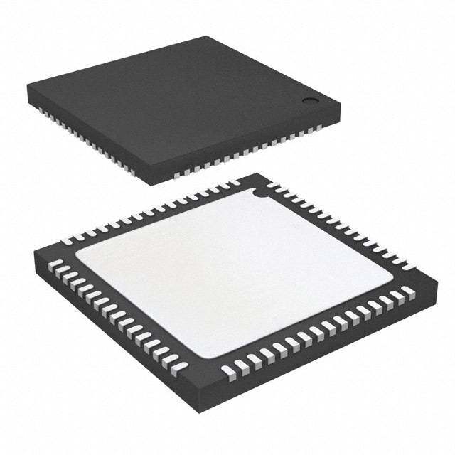
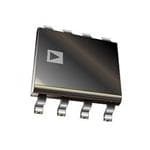
| 产品图片 |
|
| rohs | 符合RoHS无铅 / 符合限制有害物质指令(RoHS)规范要求 |
| 产品系列 | 数据转换器IC,数模转换器- DAC,Analog Devices AD5543BRZ- |
| 数据手册 | |
| 产品型号 | AD5543BRZ |
| 产品培训模块 | http://www.digikey.cn/PTM/IndividualPTM.page?site=cn&lang=zhs&ptm=19145http://www.digikey.cn/PTM/IndividualPTM.page?site=cn&lang=zhs&ptm=18614http://www.digikey.cn/PTM/IndividualPTM.page?site=cn&lang=zhs&ptm=26125http://www.digikey.cn/PTM/IndividualPTM.page?site=cn&lang=zhs&ptm=26140http://www.digikey.cn/PTM/IndividualPTM.page?site=cn&lang=zhs&ptm=26150http://www.digikey.cn/PTM/IndividualPTM.page?site=cn&lang=zhs&ptm=26146http://www.digikey.cn/PTM/IndividualPTM.page?site=cn&lang=zhs&ptm=26147 |
| 产品目录页面 | |
| 产品种类 | 数模转换器- DAC |
| 位数 | 16 |
| 供应商器件封装 | 8-SOIC |
| 分辨率 | 16 bit |
| 包装 | 管件 |
| 商标 | Analog Devices |
| 安装类型 | 表面贴装 |
| 安装风格 | SMD/SMT |
| 封装 | Tube |
| 封装/外壳 | 8-SOIC(0.154",3.90mm 宽) |
| 封装/箱体 | SOIC-8 |
| 工作温度 | -40°C ~ 85°C |
| 工厂包装数量 | 98 |
| 建立时间 | 500ns |
| 接口类型 | SPI |
| 数据接口 | 串行 |
| 最大功率耗散 | 55 uW |
| 最大工作温度 | + 85 C |
| 最小工作温度 | - 40 C |
| 标准包装 | 1 |
| 电压参考 | External |
| 电压源 | 单电源 |
| 电源电压-最大 | 5.5 V |
| 电源电压-最小 | 4.5 V |
| 积分非线性 | +/- 2 LSB |
| 稳定时间 | 500 ns |
| 系列 | AD5543 |
| 结构 | R-2R |
| 设计资源 | |
| 转换器数 | 1 |
| 转换器数量 | 1 |
| 输出数和类型 | 1 电流,单极1 电流,双极 |
| 输出类型 | Current |
| 采样比 | 1.2 MSPs |
| 采样率(每秒) | - |




- 商务部:美国ITC正式对集成电路等产品启动337调查
- 曝三星4nm工艺存在良率问题 高通将骁龙8 Gen1或转产台积电
- 太阳诱电将投资9.5亿元在常州建新厂生产MLCC 预计2023年完工
- 英特尔发布欧洲新工厂建设计划 深化IDM 2.0 战略
- 台积电先进制程称霸业界 有大客户加持明年业绩稳了
- 达到5530亿美元!SIA预计今年全球半导体销售额将创下新高
- 英特尔拟将自动驾驶子公司Mobileye上市 估值或超500亿美元
- 三星加码芯片和SET,合并消费电子和移动部门,撤换高东真等 CEO
- 三星电子宣布重大人事变动 还合并消费电子和移动部门
- 海关总署:前11个月进口集成电路产品价值2.52万亿元 增长14.8%


PDF Datasheet 数据手册内容提取
Current Output/Serial Input, 16-/14-Bit DACs Data Sheet AD5543/AD5553 FEATURES FUNCTIONAL BLOCK DIAGRAM 16-bit resolution AD5543 AD5543/AD5553 14-bit resolution AD5553 VDD RFB ±1 LSB DNL ±1 LSB INL Low noise: 12 nV/√Hz VREF DAC IOUT Low power: I = 10 µA DD 16 OR 14 0.5 µs settling time 4-quadrant multiplying reference input CONTROL DAC CS LOGIC REGISTER 2 mA full-scale current ± 20%, with V = 10 V REF Built-in R facilitates voltage conversion 16 OR 14 FB 3-wire interface CLK GND 16-BIT/14-BIT SHIFT AUlPtrPaLcoICmApTacIOt 8N-lSea d MSOP and 8-lead SOIC packages SDI REGISTER 02917-001 Figure 1. Automatic test equipment 1.0 Instrumentation 0.8 Digitally controlled calibration 0.6 Industrial control programmable logic controllers 0.4 GENERAL DESCRIPTION 0.2 B) The AD5543/AD5553 are precision 16-/14-bit, low power, S L 0 current output, small form factor digital-to-analog converters L ( N I–0.2 (DACs). They are designed to operate from a single 5 V supply with a ±10 V multiplying reference. –0.4 –0.6 The applied external reference, V , determines the full-scale REF output current. An internal feedback resistor (R ) facilitates the –0.8 FB R-2R and temperature tracking for voltage conversion when –1.0 0 6 2 8 4 0 5 2 8 4 0 6 2 8 4 0 6 9 5 8 8 8 7 7 6 6 6 5 5 4 4 4 3 cAo smerbiianl edda twa iinthte arnfa ceex toefrfnerasl hoipgehr saptieoenda, l3 a-wmipreli mfieicr.r ocontroller- 40 81 12,2 16,3 20,4 24,5 28,6CO32,7DE36,8 40,9 45,0 49,1 53,2 57,3 61,4 65,5 02917-002 Figure 2. Integral Nonlinearity (INL) compatible inputs using serial data in (SDI), clock (CLK), and chip select (CS). 2 The AD5543/AD5553 are packaged in ultracompact (3 mm × 0 4.7 mm) 8-lead MSOP and 8-lead SOIC packages. –2 –4 B) d N ( –6 AI G –8 –10 –12 –1410k 100k FREQUE1NMCY (Hz) 10M 100M 02917-025 Figure 3. Reference Multiplying Bandwidth Rev. G Document Feedback Information furnished by Analog Devices is believed to be accurate and reliable. However, no responsibility is assumed by Analog Devices for its use, nor for any infringements of patents or other One Technology Way, P.O. Box 9106, Norwood, MA 02062-9106, U.S.A. rights of third parties that may result from its use. Specifications subject to change without notice. No license is granted by implication or otherwise under any patent or patent rights of Analog Devices. Tel: 781.329.4700 ©2002–2015 Analog Devices, Inc. All rights reserved. Trademarks and registered trademarks are the property of their respective owners. Technical Support www.analog.com
AD5543/AD5553 Data Sheet TABLE OF CONTENTS Features .............................................................................................. 1 Applications Information .............................................................. 11 Applications ....................................................................................... 1 Stability ........................................................................................ 11 General Description ......................................................................... 1 Bipolar Output ............................................................................ 11 Functional Block Diagram .............................................................. 1 Programmable Current Source ................................................ 12 Revision History ............................................................................... 2 Reference Selection .................................................................... 12 Specifications ..................................................................................... 3 Amplifier Selection .................................................................... 12 Timing Diagrams .......................................................................... 4 Evaluation Board ............................................................................ 14 Absolute Maximum Ratings ............................................................ 5 System Development Platform ................................................. 14 ESD Caution .................................................................................. 5 AD5543/AD5553 to SPORT Interface .................................... 14 Pin Configuration and Function Descriptions ............................. 6 Waveform Generator ................................................................. 14 Typical Performance Characteristics ............................................. 7 Operating the Evaluation Board .............................................. 14 Circuit Operation ............................................................................. 9 Bill of Materials ........................................................................... 18 DAC Section .................................................................................. 9 Outline Dimensions ....................................................................... 19 Serial Data Interface ....................................................................... 10 Ordering Guide .......................................................................... 20 ESD Protection Circuits............................................................. 10 PCB Layout and Power Supply Bypassing .............................. 10 REVISION HISTORY 12/15—Rev. F to Rev. G 10/09—Rev. B to Rev. C Deleted Positive Output Voltage Section ..................................... 11 Updated Outline Dimensions ..................................................... 14 Changes to Ordering Guide .......................................................... 15 1/12—Rev. E to Rev. F Added Figure 15, Renumbered Sequentially ................................ 8 7/09—Rev. A to Rev. B Change to Table 9 ........................................................................... 13 Updated Format .................................................................. Universal Changes to Figure 27 ...................................................................... 15 Change to Features Section .............................................................. 1 Changes to Figure 28 ...................................................................... 16 Updated Outline Dimensions ....................................................... 14 Replaced Figure 29, Figure 30, and Figure 31 ............................. 17 Changes to Ordering Guide .......................................................... 15 2/11—Rev. D to Rev. E 2/03—Rev. 0 to Rev. A Added Evaluation Board Section.................................................. 14 Changes to Ordering Guide ............................................................. 3 Updated Outline Dimensions ....................................................... 20 Changes to Ordering Guide .......................................................... 21 12/02—Revision 0: Initial Version 4/10—Rev. C to Rev. D Changes to Figure 3 .......................................................................... 1 Changes to Table 1 ............................................................................ 3 Moved Timing Diagrams Section .................................................. 4 Moved Table 4 ................................................................................... 6 Delete Figure 13; Renumbered Sequentially ................................. 8 Changes to Figure 14 ........................................................................ 8 Changes to Figure 18 ........................................................................ 9 Moved Table 5 and Table 6 ............................................................ 10 Added Reference Selection Section and Amplifier Selection Section .............................................................................................. 12 Added Table 7, Table 8, and Table 9; Renumbered Sequentially .............................................................. 13 Rev. G | Page 2 of 20
Data Sheet AD5543/AD5553 SPECIFICATIONS V = 5 V ± 10%, V = 0 V, I = virtual GND, GND = 0 V, V = 10 V, T = full operating temperature range, unless otherwise noted. DD SS OUT REF A Table 1. Parameter Symbol Test Conditions/Comments 5 V ± 10% Unit STATIC PERFORMANCE1 Resolution N 1 LSB = V /216 = 153 μV when V = 10 V (AD5543) 16 Bits REF REF 1 LSB = V /214 = 610 μV when V = 10 V (AD5553) 14 Bits REF REF Relative Accuracy INL Grade: AD5553C ±1 LSB max Grade: AD5543C ±1 LSB max Grade: AD5543B ±2 LSB max Differential Nonlinearity (DNL) DNL Monotonic ±1 LSB max Output Leakage Current I Data = 0x0000, T = 25°C 10 nA max OUT A Data = 0x0000, T = T maximum 20 nA max A A Full-Scale Gain Error G Data = 0xFFFF ±1/±4 mV typ/max FSE Full-Scale Temperature Coefficient2 TCVFS 1 ppm/°C typ REFERENCE INPUT V Range V −15/+15 V min/max REF REF Input Resistance RREF 5 kΩ typ3 Input Capacitance2 C 5 pF typ REF ANALOG OUTPUT Output Current I Data = 0xFFFF for AD5543 2 mA typ OUT Data = 0x3FFF for AD5553 Output Capacitance2 C Code dependent 200 pF typ OUT LOGIC INPUTS AND OUTPUT Logic Input Low Voltage V 0.8 V max IL Logic Input High Voltage V 2.4 V min IH Input Leakage Current I 10 μA max IL Input Capacitance2 C 10 pF max IL INTERFACE TIMING2, 4 See Figure 4 and Figure 5 Clock Input Frequency f 50 MHz CLK Clock Width High t 10 ns min CH Clock Width Low t 10 ns min CL CS to Clock Setup t 0 ns min CSS Clock to CS Hold t 10 ns min CSH Data Setup t 5 ns min DS Data Hold t 10 ns min DH SUPPLY CHARACTERISTICS Power Supply Range V 4.5/5.5 V min/max DD RANGE Positive Supply Current I Logic inputs = 0 V 10 μA max DD Power Dissipation P Logic inputs = 0 V 0.055 mW max DISS Power Supply Sensitivity P ΔV = ±5% 0.006 %/% max SS DD Rev. G | Page 3 of 20
AD5543/AD5553 Data Sheet Parameter Symbol Test Conditions/Comments 5 V ± 10% Unit AC CHARACTERISTICS4 Output Voltage Settling Time t To ±0.1% of full scale, 0.5 µs typ S Data = 0x0000 to 0xFFFF to 0x0000 for AD5543 Data = 0x0000 to 0x3FFF to 0x0000 for AD5553 Reference Multiplying Bandwidth (BW) BW V = 100 mV rms, data = 0xFFFF 6.6 MHz typ REF DAC Glitch Impulse Q V = 0 V, data = 0x7FFF to 0x8000 for AD5543 7 nV-sec REF Feedthrough Error V /V Data = 0x0000, V = 100 mV rms, same channel −83 dB OUT REF REF Digital Feedthrough Q C = 1 and f = 1 MHz 7 nV-sec S CLK Total Harmonic Distortion THD V = 5 V p-p, data = 0xFFFF, f = 1 kHz −103 dB typ REF Output Spot Noise Voltage e f = 1 kHz, BW = 1 Hz 12 nV/√Hz N 1 All static performance tests (except IOUT) are performed in a closed-loop system using an external precision OP177 I-to-V converter amplifier. The AD5543 RFB terminal is tied to the amplifier output. The +IN operational amplifier is grounded, and the DAC IOUT is tied to the −IN operational amplifier. Typical values represent average readings measured at 25°C. 2 These parameters are guaranteed by design and are not subject to production testing. 3 All ac characteristic tests are performed in a closed-loop system using an AD8038 I-to-V converter amplifier except for THD where an AD8065 was used. 4 All input control signals are specified with tR = tF = 2.5 ns (10% to 90% of 3 V) and timed from a voltage level of 1.5 V. TIMING DIAGRAMS SDI D15 D14 D13 D12 D11 D10 D9 D8 D1 D0 CLK tDS tDH tCH tCL tCSS tCSH CS 02917-016 Figure 4. AD5543 Timing Diagram SDI D13 D12 D11 D10 D9 D8 D7 D6 D1 D0 CLK tDS tDH tCH tCL tCSS tCSH CS 02917-017 Figure 5. AD5553 Timing Diagram Rev. G | Page 4 of 20
Data Sheet AD5543/AD5553 ABSOLUTE MAXIMUM RATINGS Stresses at or above those listed under Absolute Maximum Table 2. Parameter Rating Ratings may cause permanent damage to the product. This is a stress rating only; functional operation of the product at these V to GND −0.3 V to +8 V DD or any other conditions above those indicated in the operational V to GND −18 V to +18 V REF section of this specification is not implied. Operation beyond Logic Inputs to GND −0.3 V to +8 V the maximum operating conditions for extended periods may V(I ) to GND −0.3 V to V + 0.3 V OUT DD affect product reliability. Input Current to Any Pin Except Supplies ±50 mA Package Power Dissipation (TJ Max − TA )/θJA Thermal Resistance, θ JA ESD CAUTION 8-Lead Surface Mount (MSOP) 150°C/W 8-Lead Surface Mount (SOIC) 100°C/W Maximum Junction Temperature (T ) 150°C J Max Operating Temperature Range Model B and Model C −40°C to +85°C Storage Temperature Range −65°C to +150°C Lead Temperature R-8, RM-8 (Vapor Phase, 60 sec) 215°C R-8, RM-8 (Infrared, 15 sec) 220°C Rev. G | Page 5 of 20
AD5543/AD5553 Data Sheet PIN CONFIGURATION AND FUNCTION DESCRIPTIONS CLK 1 8 CS AD5543/ SDI 2 AD5553 7 VDD VRRFEBF 34 (NToOt Pto V SIEcaWle) 56 GIONUDT 02917-004 Figure 6. Pin Configuration Table 3. Pin Function Descriptions Pin No. Mnemonic Description 1 CLK Clock Input. Positive edge triggered, clocks data into shift register. 2 SDI Serial Register Input. Data loads directly into the shift register MSB first. Extra leading bits are ignored. 3 R Internal Matching Feedback Resistor. This pin connects to an external operational amplifier for voltage output. FB 4 V DAC Reference Input Pin. Establishes DAC full-scale voltage. Constant input resistance vs. code. REF 5 I DAC Current Output. This pin connects to the inverting terminal of the external precision I-to-V operational OUT amplifier for voltage output. 6 GND Analog and Digital Ground. 7 V Positive Power Supply Input. Specified range of operation at 5 V ± 10%. DD 8 CS Chip Select. Active low digital input. Transfers shift register data to DAC register on rising edge. See Table 4 for operation. Table 4. Control Logic Truth Table CLK CS Serial Shift Register Function DAC Register X H No effect Latched ↑+1 L Shift register data advanced one bit Latched X1 H No effect Latched X1 ↑+1 Shift register data transferred to DAC register New data loaded from serial register 1 ↑+ = positive logic transition; X means don't care. Rev. G | Page 6 of 20
Data Sheet AD5543/AD5553 TYPICAL PERFORMANCE CHARACTERISTICS 1.0 1.0 0.8 0.8 0.6 0.6 0.4 0.4 B) 0.2 B)0.2 INL (LS–0.20 DNL (LS–0.02 –0.4 –0.4 –0.6 –0.6 –0.8 –0.8 –1.00 8192 16,384 24,C57O6DE3 2(,D7e6c8im4a0l,)960 49,152 57,344 65,536 02917-005 –1.00 2048 4096 61C44ODE8 (1D9e2cim1a0l,)240 12,288 14,336 16,384 02917-008 Figure 7. AD5543 INL Error Figure 10. AD5553 DNL Error 1.0 1.5 VREF = 2.5V 0.8 TA = 25°C 1.0 0.6 B) 0.4 S L 0.5 NL (LSB) 0.20 TY ERROR ( 0 DINNLL D–0.2 RI A E–0.5 –0.4 N LI –0.6 –1.0 GE –0.8 –1.00 8192 16,384 24,5C7O6DE3 2(,D7e6c8im4a0l,)960 49,152 57,344 65,536 02917-006 –1.52 4 SUPPLY VO6LTAGE VDD (V)8 10 02917-009 Figure 8. AD5543 DNL Error Figure 11. Linearity Error vs. VDD 1.0 5 VDD = 5V TA = 25°C 0.8 0.6 4 A) m 0.4 ( D D B) 0.2 NT I 3 S E L 0 R L ( UR IN–0.2 LY C 2 P –0.4 P U S –0.6 1 –0.8 –1.00 2048 4096 61C44ODE8 (1D9e2cim1a0l,)240 12,288 14,336 16,384 02917-007 00 0.5 1.0 L1O.5GIC 2IN.0PUT2V.O5LTA3G.0EVIH3 .(5V) 4.0 4.5 5.0 02917-010 Figure 9. AD5553 INL Error Figure 12. Supply Current vs. Logic Input Voltage Rev. G | Page 7 of 20
AD5543/AD5553 Data Sheet 3.0 2.5 A2 –5V DLY 67.72µs A) m2.0 T ( 0x5555 N E R R1.5 U C LY 0x8000 PP1.0 U S 0xFFFF 0x0000 0.5 010k 100kCLOCK FRE1QMUENCY (Hz)10M 100M 02917-011 5V 2V 136ns 02917-014 Figure 13. AD5543 Supply Current vs. Clock Frequency Figure 16. Settling Time –3.65 90 VDD = 5V ± 10% 80 VREF = 10V –3.70 70 –3.75 60 –3.80 SRR (dB)5400 V (V)OUT –3.85 P –3.90 30 –3.95 20 –4.00 10 010 100 FR1kEQUENCY 1(H0kz) 100k 1M 02917-012 –4.05–20 –10 0 TIM1E0 (ns) 20 30 40 02917-026 Figure 14. Power Supply Rejection Ratio (PSRR) vs. Frequency Figure 17. Midscale Transition and Digital Feedthrough 20 0 –20 B) d M ( –40 U R T –60 C E SP –80 R E W –100 O P –120 –140 –160 0 5 FR1E0QUENCY (k1H5z) 20 25 02917-200 Figure 15. AD5543/AD5553 Analog Total Harmonic Distortion (THD) Rev. G | Page 8 of 20
Data Sheet AD5543/AD5553 CIRCUIT OPERATION The AD5543/AD5553 contain a 16-/14-bit current output, Note that a matching switch is used in series with the internal DACs, serial input registers, and DAC registers. Both converters 5 kΩ feedback resistor. If users attempt to measure R , power FB use a 3-wire serial data interface. must be applied to V to achieve continuity. DD DAC SECTION VDD R2 The DAC architecture uses a current steering R-2R ladder design. Figure 18 shows the typical equivalent DAC structure. VDD RFB C1 The DAC contains a matching feedback resistor for use with an AD5543/ IOUT1 VREF VREF AD5553 A1 external operational amplifier (see Figure 19). With RFB and IOUT R1 GND VOUT = 0 TO –VREF terminals connected to the operational amplifier output and SYNC SCLK SDIN inverting node, respectively, a precision voltage output is AGND achieved as µCONTROLLER V = −V × D/65,536 (AD5543) (1) OUT REF NOTES VOUT = −VREF × D/16,384 (AD5553) (2) 12..RCIF11 A AP1HN IADSS RAE2 H CUIOGSMHE DPS EPONENSELADYT AIIOFM NGP AL(4IIpFNFI EA TRDO.J U6SpTFM) MENATY IBSE R REEQQUUIRIREEDD. 02917-019 Note that the output voltage polarity is the opposite of the VREF Figure 19. Voltage Output Configuration polarity for dc reference voltages. These DACs are also designed to accommodate ac reference These DACs are designed to operate with either negative or input signals. The AD5543 accommodates input reference positive reference voltages. The VDD power pin is only used by voltages in the range of −12 V to +12 V. The reference voltage the internal logic to drive the on and off states of the DAC switches. inputs exhibit a constant nominal input resistance value of 5 kΩ ± 30%. The DAC output (I ) is code dependent, producing OUT VDD various resistances and capacitances. External amplifier choice R R R VREF RFB must take into account the variation in impedance generated by 2R 2R 2R R 5kΩ the AD5543 on the inverting input node of the amplifier. The S2 S1 feedback resistance, in parallel with the DAC ladder resistance, IOUT dominates output voltage noise. To maintain good analog perf- ormance, power supply bypassing of 0.01 µF to 0.1 µF ceramic or GND chip capacitors, in parallel with a 1 µF tantalum capacitor, is recommended. Due to degradation of PSRR in frequency, users DSWIGIITTCAHLE ISN TSE1R AFNADC ES 2C AORNEN ECCLTOISOENDS, OVDMDIT MTUESDT F BOER PCOLWAREIRTEYD;. 02917-018 must avoid using switching power supplies. Figure 18. Equivalent R-2R DAC Circuit Rev. G | Page 9 of 20
AD5543/AD5553 Data Sheet SERIAL DATA INTERFACE The AD5543/AD5553 use a 3-wire (CS, SDI, CLK) serial data VDD interface. New serial data is clocked into the serial input register DIGITAL INPUTS in a 16-bit data-word format for the AD5543. The MSB is loaded first. Table 5 defines the 16 data-word bits. Data is placed on the 5kΩ SDI pin and clocked into the register on the positive clock edge othf aCt LarKe, sspuebcjiefciet dto i nth teh ed aintat esreftaucpe- tainmdi-nhgo sldp etcimifiec arteiqounisr.e Omnelnyt sth e DGND 02917-020 Figure 20. Equivalent ESD Protection Circuits last 16 bits clocked into the serial register are interrogated when the CS pin is strobed to transfer the serial register data to the DAC PCB LAYOUT AND POWER SUPPLY BYPASSING register. Because most microcontrollers output serial data in 8- It is a good practice to employ compact, minimum lead length bit bytes, two data bytes can be written to the AD5543/AD5553. printed circuit board (PCB) layout design. The leads to the After loading the serial register, the rising edge of CS transfers input must be as short as possible to minimize infrared drop the serial register data to the DAC register; during this strobe, and stray inductance. the CLK must not be toggled. For the AD5553, with 16-bit clock It is also essential to bypass the power supplies with quality cycles, the two LSBs are ignored. capacitors for optimum stability. Supply leads to the device ESD PROTECTION CIRCUITS must be bypassed with 0.01 µF to 0.1 µF disc or chip ceramic capacitors. Low ESR 1 µF to 10 µF tantalum or electrolytic All logic input pins contain back-biased ESD protection Zener capacitors must also be applied at the supplies to minimize diodes that are connected to ground (DGND) and V , as DD transient disturbance and filter out low frequency ripple. shown in Figure 20. The PCB metal traces between V and R must also be REF FB matched to minimize gain error. Table 5. AD5543 Serial Input Register Data Format; Data Loaded MSB First Format B15 (MSB) B14 B13 B12 B11 B10 B9 B8 B7 B6 B5 B4 B3 B2 B1 B0 (LSB) D15 D14 D13 D12 D11 D10 D9 D8 D7 D6 D5 D4 D3 D2 D1 D0 Table 6. AD5553 Serial Input Register Data Format; Data Loaded MSB First Format B13 (MSB)1 B12 B11 B10 B9 B8 B7 B6 B5 B4 B3 B2 B1 B0 (LSB) D13 D12 D11 D10 D9 D8 D7 D6 D5 D4 D3 D2 D1 D0 1 A full 16-bit data-word can be loaded into the AD5553 serial input register, but only the last 14 bits entered are transferred to the DAC register when CS returns to logic high. Rev. G | Page 10 of 20
Data Sheet AD5543/AD5553 APPLICATIONS INFORMATION STABILITY BIPOLAR OUTPUT VDD The AD5543/AD5553 are inherently 2-quadrant multiplying U1 C1 DACs. That is, they can easily be set up for unipolar output VDD RFB operation. The full-scale output polarity is the inverse of the VREF VREF IOUT reference input voltage. VO AD8628 In some applications, it may be necessary to generate the full GND AD5543/AD5553 U2 02917-021 4is- eqausaidlyr aancct ommupltliipshlyeidn gb yc aupsainbgil iatyn oard ad ibtiiopnoalal rU o4u tepxutet rsnwailn agm, wplhifiicehr Figure 21. Optional Compensation Capacitor for Gain Peaking Prevention configured as a summing amplifier (see Figure 22). In this circuit, the second amplifier, U4, provides a gain of 2 that increases the In the I-to-V configuration, the I of the DAC and the inverting OUT output span magnitude to 5 V. Biasing the external amplifier with a node of the operational amplifier must be connected as close as 2.5 V offset from the reference voltage results in a full 4-quadrant possible to each other, and proper PCB layout technique must be multiplying circuit. The transfer equation of this circuit shows employed. Because every code change corresponds to a step that both negative and positive output voltages are created as the function, gain peaking may occur if the operational amplifier has input data (D) is incremented from code zero (V = −2.5 V) OUT limited gain bandwidth product (GBP) and there is excessive to midscale (V = 0 V) to full-scale (V = +2.5 V). OUT OUT parasitic capacitance at the inverting node. V = (D/32,768 − 1) × V (AD5543) (3) OUT REF An optional compensation capacitor, C1, can be added for stability, as shown in Figure 21. C1 must be found empirically, VOUT = (D/16,384 − 1) × VREF (AD5553) (4) but 20 pF is generally adequate for the compensation. For the AD5543, the resistance tolerance becomes the dominant error of which users must be aware. R1 R2 10kΩ ± 0.01% 10kΩ ± 0.01% C2 U4 +5V +5V 5kΩ ± 0.01% ADR03 U1 R3 1/2AVD+8620 VO VDD RFB C1 V– +5V VOUTVIN VREF IOUT GND GND 1/2AD8620 –2.5V <– 5VVO < +2.5V U3 AD5553 ONLY U2 02917-023 Figure 22. 4-Quadrant Multiplying Application Circuit Rev. G | Page 11 of 20
AD5543/AD5553 Data Sheet PROGRAMMABLE CURRENT SOURCE REFERENCE SELECTION Figure 23 shows a versatile V-I conversion circuit using an When selecting a reference for use with the AD5543/AD5553 improved Howland current pump. In addition to the precision and other devices in this series of current output DACs, pay current conversion it provides, this circuit enables a bidirectional attention to the output voltage temperature coefficient reference. current flow and high voltage compliance. This circuit can be used Choosing a precision reference with a low output temperature in 4 mA to 20 mA current transmitters with up to 500 Ω of load. In coefficient minimizes error sources. Table 7 lists some of the Figure 23, it can be shown that if the resistor network is matched, references available from Analog Devices, Inc., that are suitable the load current is for use with this range of current output DACs. (R2+R3)/R1 AMPLIFIER SELECTION I = ×V ×D (5) L R3 REF The primary requirement for the current steering mode is an R3 in theory can be made small to achieve the current needed amplifier with low input bias currents and low input offset within the U3 output current driving capability. This circuit is voltage. Because of the code dependent output resistance of the versatile such that AD8510 can deliver ±20 mA in both directions DAC, the input offset voltage of an operational amplifier is and the voltage compliance approaches 15 V, which is limited multiplied by the variable gain of the circuit. A change in this noise mainly by the supply voltages of U3. However, users must pay gain between two adjacent digital fractions produces a step attention to the compensation. Without C1, it can be shown change in the output voltage due to the amplifier input offset that the output impedance becomes voltage. This output voltage change is superimposed upon the R1'R3(R1+R2) desired change in output between the two codes and gives rise ZO = R1(R2'+R3')−R1'(R2+R3) (6) to a differential linearity error, which, if large enough, can cause the DAC to be nonmonotonic. If the resistors are perfectly matched, Z is infinite, which is O The input bias current of an operational amplifier also generates desirable, and behaves as an ideal current source. On the other an offset at the voltage output because of the bias current flowing in hand, if the resistors are not matched, Z can be either positive or O the feedback resistor, R . negative. Negative can cause oscillation. As a result, C1 is needed to FB prevent the oscillation. For critical applications, C1 can be found Common-mode rejection of the operational amplifier is empirically but typically falls in the range of a few picofarads (pF). important in voltage switching circuits because it produces a code dependent error at the voltage output of the circuit. VDD Provided that the DAC switches are driven from true wideband U1 VDD RFB low impedance sources (VIN and AGND), they settle quickly. VREF VREF IOUT R1' R2' Consequently, the slew rate and settling time of a voltage switching 150kΩ 15kΩ GND AD8628 DAC circuit is determined largely by the output operational C1 amplifier. To obtain minimum settling time in this configuration, AD5543/AD5553 10pF minimize capacitance at the V node (the voltage output node U2 REF VDD R3' in this application) of the DAC. This is done by using low input U3 50Ω capacitance buffer amplifiers and careful board design. V+ AD8510 Analog Devices offers a wide range of amplifiers for both V– R3 precision dc and ac applications, as listed in Table 8 and Table 9. 50Ω VSS VL R1 R2 150kΩ 15kΩ LOAD IL 02917-024 Figure 23. Programmable Current Source with Bidirectional Current Control and High Voltage Compliance Capabilities Rev. G | Page 12 of 20
Data Sheet AD5543/AD5553 Table 7. Suitable Analog Devices Precision References Maximum Temperature Part No. Output Voltage (V) Initial Tolerance (%) Drift (ppm/°C) I (mA) Output Noise (µV p-p) Packages SS ADR01 10 0.05 3 1 20 SOIC-8 ADR01 10 0.05 9 1 20 TSOT-5, SC70-5 ADR02 5.0 0.06 3 1 10 SOIC-8 ADR02 5.0 0.06 9 1 10 TSOT-5, SC70-5 ADR03 2.5 0.1 3 1 6 SOIC-8 ADR03 2.5 0.1 9 1 6 TSOT-5, SC70-5 ADR06 3.0 0.1 3 1 10 SOIC-8 ADR06 3.0 0.1 9 1 10 TSOT-5, SC70-5 ADR420 2.048 0.05 3 0.5 1.75 SOIC-8, MSOP-8 ADR421 2.50 0.04 3 0.5 1.75 SOIC-8, MSOP-8 ADR423 3.00 0.04 3 0.5 2 SOIC-8, MSOP-8 ADR425 5.00 0.04 3 0.5 3.4 SOIC-8, MSOP-8 ADR431 2.500 0.04 3 0.8 3.5 SOIC-8, MSOP-8 ADR435 5.000 0.04 3 0.8 8 SOIC-8, MSOP-8 ADR391 2.5 0.16 9 0.12 5 TSOT-5 ADR395 5.0 0.10 9 0.12 8 TSOT-5 Table 8. Suitable Analog Devices Precision Operational Amplifier 0.1 Hz to 10 Hz Part No. Supply Voltage (V) VOS Maximum (µV) IB Maximum (nA) Noise (µV p-p) Supply Current (µA) Packages OP97 ±2 to ±20 25 0.1 0.5 600 SOIC-8 , PDIP-8 OP1177 ±2.5 to ±15 60 2 0.4 500 MSOP-8, SOIC-8 AD8675 ±5 to ±18 75 2 0.1 2300 MSOP-8, SOIC-8 AD8671 ±5 to ±15 75 12 0.077 3000 MSOP-8, SOIC-8 ADA4004-1 ±5 to ±15 125 90 0.1 2000 SOIC-8, SOT-23-5 AD8603 1.8 to 5 50 0.001 2.3 40 TSOT-5 AD8607 1.8 to 5 50 0.001 2.3 40 MSOP-8, SOIC-8 AD8605 2.7 to 5 65 0.001 2.3 1000 WLCSP-5, SOT-23-5 AD8615 2.7 to 5 65 0.001 2.4 2000 TSOT-5 AD8616 2.7 to 5 65 0.001 2.4 2000 MSOP-8, SOIC-8 Table 9. Suitable Analog Devices High Speed Operational Amplifier Part No. Supply Voltage (V) BW at ACL (MHz) Slew Rate (V/µs) V (Max) (µV) I (Max) (nA) Packages OS B AD8065 5 to 24 145 180 1500 0.006 SOIC-8, SOT-23-5 AD8066 5 to 24 145 180 1500 0.006 SOIC-8, MSOP-8 AD8021 5 to 24 490 120 1000 10,500 SOIC-8, MSOP-8 AD8038 3 to 12 350 425 3000 750 SOIC-8, SC70-5 ADA4899-1 5 to 12 600 310 35 100 LFCSP-8, SOIC-8 AD8057 3 to 12 325 1000 5000 500 SOT-23-5, SOIC-8 AD8058 3 to 12 325 850 5000 500 SOIC-8, MSOP-8 AD8061 2.7 to 8 320 650 6000 350 SOT-23-5, SOIC-8 AD8062 2.7 to 8 320 650 6000 350 SOIC-8, MSOP-8 AD9631 ±3 to ±6 320 1300 10,000 7000 SOIC-8, PDIP-8 Rev. G | Page 13 of 20
AD5543/AD5553 Data Sheet EVALUATION BOARD The EVAL-AD5543/EVAL-AD5553 is used in conjunction with SPORT_TFS CS an SDP1Z system development platform board available from Analog Devices, which is purchased separately from the evaluation SPORT_TSCLK SCLK board. The USB to serial peripheral interface (SPI) communication SPORT_DTO SDIN to the AD5543 is completed using this Blackfin-based development board. The software offers a waveform generator. SYSTEM DEVELOPMENT PLATFORM The system development platform (SDP) is a hardware and ADSP-BF527 AD5543/AD5553 02917-124 software evaluation tool for use in conjunction with product Figure 24. AD5543/AD5553 to SPORT Interface evaluation boards. The SDP board is based on the Blackfin WAVEFORM GENERATOR ADSP-BF527 processor with USB connectivity to the PC through a USB 2.0 high speed port. For more information about The evaluation board software offers a waveform generator to this device, see the system development platform web page. show every change introduced and transmitted to the output. AD5543/AD5553 TO SPORT INTERFACE OPERATING THE EVALUATION BOARD The Analog Devices SDP has one SPORT serial port. The The evaluation board requires ±12 V and +5 V supplies. The SPORT interface is used to control the AD5543/AD5553, +12 V VDD and VSS are used to power the output amplifier, while allowing clock frequencies up to 30 MHz. the +5 V is used to power the DAC (VDD1). 02917-125 Figure 25. Evaluation Board Software—Waveform Generator Rev. G | Page 14 of 20
Data Sheet AD5543/AD5553 621-71920 T U O V J4 T U O V 10uF + 0.1uF 10uF 0.1uF 6 + C4 C5 OP C6 C7 4 7 V-V+ U3 DIS8 SS - + DD V 2 3 V F RE J3 F V p C35.6 Y L P P U S E C DP EN uF uF DAC + VIN FOR S OP AMP + REFER DVDD C110+ C20.1 7VDD U1 3RFBSCLK 5IOUTSDIN 4VREFCS AD5543_53 AGND6 LK16 C10 0.1uF AGND 1 2 8 UT J1-1 J1-2 J1-5 J1-4 J1-3 /CS VO U2R435 D 4 SDIN +VIN ADTRIMGN ND SCLK 2 5C90.1uF G D D D V D DD SS DD + V V V C8uF 10 K N S SCL SDI /C Figure 26. Schematic of AD5543/AD5553 Evaluation Board Rev. G | Page 15 of 20
AD5543/AD5553 Data Sheet BMODE1: PULL UP WITH A 10k RESISTOR TO SET SDP TO BOOT FROM A SPI FLASH ON THE DAUGHTER BOARD J2 60 61 RESET_IN BMODE1 59 62 58 UART_RX UART_TX 63 57 GND GND 64 NC NC BOARD ID EEPROM (24LC64) MUST BE ON I2C BUS 0, ADDRESS IS AT USER DISCRETION 55556543 NNNCCC CSOTNASNNDEDPCATRODR NNNCCC 66668765 3.3V_BF U4 NC NC 52 69 1 8 GND GND A0 VCC 51 70 2 7 NC NC A1 WP 50 71 3 6 NC NC A2 SCL 49 TMR_C* TMR_D 72 4 VSS SDA 5 444876 TGMPIRO_6A TIMERS TGMPRIO_B7 777543 24LC64 45 GGNPIDO4 GENERAL GPGINOD5 76 4443 GPIO2 INPUT/OUTPUT GPIO3 7787 STATUS 42 GPIO0 GPIO1 79 START SCL_1 SCL_0 41 SDA_1 I2C SDA_0 80 40 81 3398 GSPNID_SEL1/SPI_SS SPI_GCNLDK 8832 MAIN I2C BUS (CONNECTED TO BLACKFIN TWI - PULL UP RESISTORS NOT REQUIRED) 333765 SSGPPNIID__SSEELL__CB SPI SSSPPPI_IIS__MMELOIS_SOAI 888654 I(2CCO BNUNSE C1T IESD C TOOM BMLOANC KAFCIRNO GSPSI OB O- TUHS EC OI2NCN_0E CFTIROSRTS) ON SDP - PULL UP RESISTORS REQUIRED 33334321 SSSSPPPPOOOORRRRTTTT____IDDDNTTTT321** SPORT SPOSSPPROOT_RRTTTS__GCTDNLFTDKS0 98880987 SS/CCDSLINK 322098 SSSPPPOOORRRTTT___DDDRRR123** SPOSSPPROOT_RRRTTS__CDRLRFKS0 999321 27 GND GND 94 26 PAR_FS1 PAR_CLK 95 25 PAR_FS3 PAR_FS2 96 24 PAR_A1 PAR_A0 97 23 PAR_A3 PAR_A2 98 22 GND GND 99 21 PAR_CS PAR_INT 100 20 PAR_RD PAR_WR 101 PAR_D1 PAR_D0 19 PAR_D3 PARALLEL PAR_D2 102 18 PAR_D5 PORT PAR_D4 103 17 104 GND GND 16 105 PAR_D7 PAR_D6 15 106 14 PAR_D9 PAR_D8 107 13 PAR_D11 PAR_D10 108 12 PAR_D13 PAR_D12 109 PAR_D14 GND 11 110 USB_VBUS GND PAR_D15 10 PAR_D17 * *PAR_D16 111 9 PAR_D19 * *PAR_D18 112 8 PAR_D21 * *PAR_D20 113 3.3V_BF 76 PAR_D23 * *PAR_D22 111154 54 GUSNBD_VBUS VIO(+3G.3NVD) 111176 VIO: USE TO SET IO VOLTAGE MAX DRAW 20mA VRIENQ: UUISREE ST H4I-S7 VP I2N0 0TmOA POWER THE SDP 32 GGNNDD GGNNDD 111198 1 NVICN *NC ON BLACKFIN SDP NNCC 120 02917-127 Figure 27. Schematic of SDP Interface Rev. G | Page 16 of 20
Data Sheet AD5543/AD5553 02917-128 Figure 28. Silkscreen—Component Side View (Top Layer) 02917-129 Figure 29. Component Side Artwork 02917-130 Figure 30. Solder Side Artwork Rev. G | Page 17 of 20
AD5543/AD5553 Data Sheet BILL OF MATERIALS Table 10. Name Part Description Value PCB Decal Part Description CS Test point Test point Red test point AGND Test point Test point Black test point C1 Capacitor+ 10 µF RTAJ_A 10 V SMD tantalum capacitor C2 Capacitor 0.1 µF C0603 50 V X7R ceramic capacitor C3 Capacitor 5.6 pF C0603 Multilayer ceramic capacitor C4 Capacitor+ 10 µF RTAJ_B 16 V tantalum capacitor C5 Capacitor 0.1 µF C0603 50 V X7R ceramic capacitor C6 Capacitor+ 10 µF RTAJ_B 16 V tantalum capacitor C7 Capacitor 0.1 µF C0603 50 V X7R ceramic capacitor C8 Capacitor+ 10 µF RTAJ_B 16 V tantalum capacitor C9 Capacitor 0.1 µF C0603 50 V X7R ceramic capacitor C10 Capacitor 0.1 µF C0603 50 V X7R ceramic capacitor C11 Capacitor 10 µF C0805 10 V 10 µF ceramic capacitor 10% X5R 0805 C12 Capacitor 0.1 µF C0603 50 V X7R ceramic capacitor GL1 Ground link Component link Copper short J1 CON\POWER5 CON\POWER5 5-pin terminal block J2 SDP-STANDARD-CONN CON-120/FX8-120S-SV 120-way connector, 0.6 mm pitch, receptacle J3 SMB SMB Straight PCB mount SMB jack—50 Ω J4 SMB SMB Straight PCB mount SMB jack—50 Ω SCLK Test point Test point Red test point SDIN Test point Test point Red testpoint U1 AD5543/AD5553 SO8NB Digital-to-analog converter U2 ADR435 SO8NB 5 V reference U3 AD8038 SO8NB Single operational amplifier 8-pin U4 24LC64 MSO8 64K I2C serial EEPROM MSOP8 USB_VBUS Test point Test point Black test point VOUT Test point Test point Red test point VREF Test point Test point Red test point X1 MTHOLE-3MM MTHOLE-3MM 3 mm NPTH hole X2 MTHOLE-3MM MTHOLE-3MM 3 mm NPTH hole Rev. G | Page 18 of 20
Data Sheet AD5543/AD5553 OUTLINE DIMENSIONS 3.20 3.00 2.80 8 5 5.15 3.20 4.90 3.00 4.65 2.80 1 4 PIN1 IDENTIFIER 0.65BSC 0.95 15°MAX 0.85 1.10MAX 0.75 0.80 0.15 0.40 6° 0.23 0.55 CO0P.0L50A.1N0ARICTOYMPLIANT0.T25OJEDECSTA0°NDARDS0M.0O9-187-AA 0.40 10-07-2009-B Figure 31. 8-Lead Mini Small Outline Package [MSOP] (RM-8) Dimensions shown in millimeters 5.00(0.1968) 4.80(0.1890) 8 5 4.00(0.1574) 6.20(0.2441) 3.80(0.1497) 1 4 5.80(0.2284) 1.27(0.0500) 0.50(0.0196) BSC 1.75(0.0688) 0.25(0.0099) 45° 0.25(0.0098) 1.35(0.0532) 8° 0.10(0.0040) 0° COPLANARITY 0.51(0.0201) 0.10 SEATING 0.31(0.0122) 0.25(0.0098) 10..2470((00..00510507)) PLANE 0.17(0.0067) COMPLIANTTOJEDECSTANDARDSMS-012-AA (RCINEOFNPEATRRREOENNLCLTEIHNEOGSNDELISYM)AEANNRDSEIAORRNOESUNANORDETEDAIN-POMPFRIFLOLMPIMIRLELIATIMTEEERTFSEO;RIRNECUQHSUEDIVIINMAELDENENSSTIIOGSNNFS.OR 012407-A Figure 32. 8-Lead Standard Small Outline Package [SOIC_N] Narrow Body (R-8) Dimensions shown in millimeters and (inches) Rev. G | Page 19 of 20
AD5543/AD5553 Data Sheet ORDERING GUIDE Model1, 2 INL (LSB) RES (LSB) Temperature Range Package Description Package Option Branding AD5543CRMZ ±1 16 −40°C to +85°C 8-Lead MSOP RM-8 DEV AD5543CRMZ-REEL7 ±1 16 −40°C to +85°C 8-Lead MSOP RM-8 DEV AD5543BR ±2 16 −40°C to +85°C 8-Lead SOIC_N R-8 AD5543BRZ ±2 16 −40°C to +85°C 8-Lead SOIC_N R-8 AD5543BRM ±2 16 −40°C to +85°C 8-Lead MSOP RM-8 DXB AD5543BRMZ ±2 16 −40°C to +85°C 8-Lead MSOP RM-8 DXB# AD5543BRMZ-REEL7 ±2 16 −40°C to +85°C 8-Lead MSOP RM-8 DXB# AD5553CRM ±1 14 −40°C to +85°C 8-Lead MSOP RM-8 DUC AD5553CRM-REEL7 ±1 14 −40°C to +85°C 8-Lead MSOP RM-8 DUC AD5553CRMZ ±1 14 −40°C to +85°C 8-Lead MSOP RM-8 DUC# AD5553CRMZ-REEL7 ±1 14 −40°C to +85°C 8-Lead MSOP RM-8 DUC# EVAL-AD5543SDZ Evaluation Board 1 The AD5543 contains 1040 transistors. The die size measures 55 mil × 73 mil or 4,015 sq. mil. 2 Z = RoHS Compliant Part, # denotes RoHS-compliant product may be top or bottom marked. I2C refers to a communications protocol originally developed by Philips Semiconductors (now NXP Semiconductors). ©2002–2015 Analog Devices, Inc. All rights reserved. Trademarks and registered trademarks are the property of their respective owners. D02917-0-12/15(G) Rev. G | Page 20 of 20
Mouser Electronics Authorized Distributor Click to View Pricing, Inventory, Delivery & Lifecycle Information: A nalog Devices Inc.: EVAL-AD5543SDZ AD5543BRMZ-REEL7 AD5543BRM AD5543CRMZ-REEL7 AD5553CRMZ AD5543SRMZ-EP AD5543CRMZ AD5553CRM AD5543BR AD5543BRMZ AD5543BRZ AD5553CRMZ-REEL7
 Datasheet下载
