ICGOO在线商城 > 集成电路(IC) > 数据采集 - 数模转换器 > DAC8562SDSCT
 Datasheet下载
- 型号: DAC8562SDSCT
- 制造商: Texas Instruments
- 库位|库存: xxxx|xxxx
- 要求:
| 数量阶梯 | 香港交货 | 国内含税 |
| +xxxx | $xxxx | ¥xxxx |
查看当月历史价格
查看今年历史价格
DAC8562SDSCT产品简介:
ICGOO电子元器件商城为您提供DAC8562SDSCT由Texas Instruments设计生产,在icgoo商城现货销售,并且可以通过原厂、代理商等渠道进行代购。 DAC8562SDSCT价格参考¥36.54-¥67.88。Texas InstrumentsDAC8562SDSCT封装/规格:数据采集 - 数模转换器, 16 位 数模转换器 2 10-WSON(3x3)。您可以下载DAC8562SDSCT参考资料、Datasheet数据手册功能说明书,资料中有DAC8562SDSCT 详细功能的应用电路图电压和使用方法及教程。
Texas Instruments(德州仪器)的DAC8562SDSCT是一款16位双通道电压输出数模转换器(DAC),属于数据采集系统中的数模转换器类别。其应用场景主要包括以下领域:

1. 工业自动化与控制
   DAC8562SDSCT可用于工业控制系统中,将数字信号转换为精确的模拟信号,用于驱动执行器、传感器或调节装置。例如,在PID控制器中,它可以生成精确的电压信号来调整电机速度或阀门开度。

2. 测试与测量设备
   在精密测试仪器中,如信号发生器或校准设备,DAC8562提供高分辨率和低噪声的输出,能够生成高质量的模拟波形,满足对精度要求较高的测量需求。

3. 医疗设备
   该器件适用于需要高精度信号生成的医疗设备,如超声波成像设备、心电图仪或其他诊断工具,用于生成稳定的刺激信号或控制模拟前端电路。

4. 通信系统
   在通信领域,DAC8562可用于生成调制信号或控制射频前端的增益和偏置设置,支持高性能通信模块的设计。

5. 音频处理
   虽然主要用于工业应用,但其高分辨率和低失真特性也使其适合某些高端音频应用,例如专业音频设备中的数字信号还原。

6. 汽车电子
   在汽车行业中,DAC8562可以用于车载信息娱乐系统、传感器接口或动力总成控制单元(PCM)中,实现精确的模拟信号生成。

7. 可编程逻辑控制器(PLC)
   DAC8562可用于PLC中,将数字指令转换为模拟信号以控制外部设备,如变频器或液压系统。

总结来说,DAC8562SDSCT凭借其高精度、低功耗和双通道设计,广泛应用于需要精确模拟信号生成的各种场景,特别适合对性能和可靠性要求较高的工业、医疗和通信领域。
| 参数 | 数值 |
| 产品目录 | 集成电路 (IC)半导体 |
| 描述 | IC DAC 16BIT SRL DUAL 10WSON数模转换器- DAC 16B,Dual,Lo Pwr Ultra-Lo Glitch DAC |
| 产品分类 | |
| 品牌 | Texas Instruments |
| 产品手册 | http://www.ti.com/lit/gpn/dac8562 |
| 产品图片 | |
| rohs | 符合RoHS无铅 / 符合限制有害物质指令(RoHS)规范要求 |
| 产品系列 | 数据转换器IC,数模转换器- DAC,Texas Instruments DAC8562SDSCT- |
| 数据手册 | 点击此处下载产品Datasheethttp://www.ti.com/lit/pdf/slyb174 |
| 产品型号 | DAC8562SDSCT |
| 产品种类 | 数模转换器- DAC |
| 位数 | 16 |
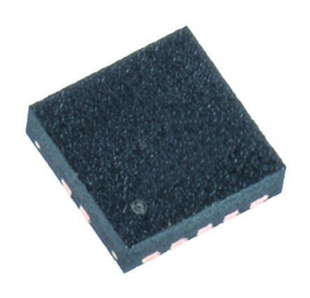
| 供应商器件封装 | 10-WSON (3x3) |
| 其它名称 | 296-29098-2 |
| 分辨率 | 16 bit |
| 制造商产品页 | http://www.ti.com/general/docs/suppproductinfo.tsp?distId=10&orderablePartNumber=DAC8562SDSCT |
| 包装 | 带卷 (TR) |
| 商标 | Texas Instruments |
| 安装类型 | 表面贴装 |
| 安装风格 | SMD/SMT |
| 封装 | Reel |
| 封装/外壳 | 10-WFDFN 裸露焊盘 |
| 封装/箱体 | WSON-10 |
| 工作温度 | -40°C ~ 125°C |
| 工厂包装数量 | 250 |
| 建立时间 | 10µs |
| 接口类型 | Serial (3-Wire) |
| 数据接口 | DSP,MICROWIRE™,QSPI™,串行,SPI™ |
| 最大工作温度 | + 125 C |
| 标准包装 | 250 |
| 电压源 | 单电源 |
| 电源电压-最大 | 5.5 V |
| 电源电压-最小 | 2.7 V |
| 稳定时间 | 10 us |
| 系列 | DAC8562 |
| 转换器数 | 2 |
| 转换器数量 | 2 |
| 输出数和类型 | 2 电压,单极 |
| 采样率(每秒) | - |


- 商务部:美国ITC正式对集成电路等产品启动337调查
- 曝三星4nm工艺存在良率问题 高通将骁龙8 Gen1或转产台积电
- 太阳诱电将投资9.5亿元在常州建新厂生产MLCC 预计2023年完工
- 英特尔发布欧洲新工厂建设计划 深化IDM 2.0 战略
- 台积电先进制程称霸业界 有大客户加持明年业绩稳了
- 达到5530亿美元!SIA预计今年全球半导体销售额将创下新高
- 英特尔拟将自动驾驶子公司Mobileye上市 估值或超500亿美元
- 三星加码芯片和SET,合并消费电子和移动部门,撤换高东真等 CEO
- 三星电子宣布重大人事变动 还合并消费电子和移动部门
- 海关总署:前11个月进口集成电路产品价值2.52万亿元 增长14.8%


PDF Datasheet 数据手册内容提取
Product Sample & Technical Tools & Support & Reference Folder Buy Documents Software Community Design DAC7562,DAC7563,DAC8162 DAC8163,DAC8562,DAC8563 SLAS719E–AUGUST2010–REVISEDJUNE2015 DACxx6x Dual 16-, 14-, 12-Bit, Low-Power, Buffered, Voltage-Output DACs With 2.5-V, 4-PPM/°C Internal Reference 1 Features 3 Description • RelativeAccuracy: The DAC756x, DAC816x, and DAC856x devices are 1 low-power, voltage-output, dual-channel, 16-, 14-, – DAC756x(12-Bit):0.3LSBINL and 12-bit digital-to-analog converters (DACs), – DAC816x(14-Bit):1LSBINL respectively. These devices include a 2.5-V, – DAC856x(16-Bit):4LSBINL 4-ppm/°C internal reference, giving a full-scale output voltage range of 2.5 V or 5 V. The internal reference • GlitchImpulse:0.1nV-s has an initial accuracy of ±5 mV and can source or • BidirectionalReference:Inputor2.5-VOutput sinkupto20mAattheV /V pin. REFIN REFOUT – OutputDisabledbyDefault These devices are monotonic, providing excellent – ±5-mVInitialAccuracy(Max) linearity and minimizing undesired code-to-code – 4-ppm°CTemperatureDrift(Typ) transient voltages (glitch). They use a versatile three- wire serial interface that operates at clock rates up to – 10-ppm/°CTemperatureDrift(Max) 50 MHz. The interface is compatible with standard – 20-mASinkandSourceCapability SPI™, QSPI™, Microwire, and digital signal • Power-OnResettoZeroScaleorMid-Scale processor (DSP) interfaces. The DACxx62 devices incorporate a power-on-reset circuit that ensures the • Low-Power:4mW(Typ,5-VAV ,Including DD DAC output powers up and remains at zero scale InternalReferenceCurrent) until a valid code is written to the device, whereas the • WidePower-SupplyRange:2.7Vto5.5V DACxx63 devices similarly power up at mid-scale. • 50-MHzSPIWithSchmitt-TriggeredInputs These devices contain a power-down feature that reduces current consumption to typically 550 nA at • LDACandCLRFunctions 5 V. The low power consumption, internal reference, • OutputBufferWithRail-to-RailOperation and small footprint make these devices ideal for • Packages:WSON-10(3mm ×3mm),VSSOP-10 portable,battery-operatedequipment. • TemperatureRange:–40°Cto125°C The DACxx62 devices are drop-in and function- compatible with each other, as are the DACxx63 2 Applications devices. The entire family is available in MSOP-10 andSON-10packages. • PortableInstrumentation • PLCAnalogOutputModule DeviceInformation(1) • Closed-LoopServoControl PARTNUMBER PACKAGE BODYSIZE(NOM) • VoltageControlledOscillatorTuning DAC8562 • DataAcquisitionSystems DAC8162 VSSOP(10), 3.00mm×3.00mm WSON(10) • ProgrammableGainandOffsetAdjustment DAC7562 (1) For all available packages, see the orderable addendum at theendofthedatasheet. SimplifiedBlockDiagram GND AVDD LDAC CLR VREFIN/VREFOUT DIN Buffer Control Register Control 2.5-V PDoowwenr- SCLK Input Control Logic Reference Control SYNC Control Logic Logic Data Buffer B DAC Register B DAC VOUTB DAC756x (12-Bit) DAC816x (14-Bit) Data BufferA DAC RegisterA DAC VOUTA DAC856x (16-Bit) 1 An IMPORTANT NOTICE at the end of this data sheet addresses availability, warranty, changes, use in safety-critical applications, intellectualpropertymattersandotherimportantdisclaimers.PRODUCTIONDATA.
DAC7562,DAC7563,DAC8162 DAC8163,DAC8562,DAC8563 SLAS719E–AUGUST2010–REVISEDJUNE2015 www.ti.com Table of Contents 1 Features.................................................................. 1 8.4 DeviceFunctionalModes........................................32 2 Applications........................................................... 1 8.5 Programming...........................................................36 3 Description............................................................. 1 9 ApplicationandImplementation........................ 39 4 RevisionHistory..................................................... 2 9.1 ApplicationInformation............................................39 9.2 TypicalApplications................................................41 5 DeviceComparisonTable..................................... 3 9.3 SystemExamples...................................................45 6 PinConfigurationandFunctions......................... 4 10 PowerSupplyRecommendations..................... 46 7 Specifications......................................................... 5 11 Layout................................................................... 46 7.1 AbsoluteMaximumRatings......................................5 11.1 LayoutGuidelines.................................................46 7.2 ESDRatings ............................................................5 11.2 LayoutExample....................................................47 7.3 RecommendedOperatingConditions.......................5 12 DeviceandDocumentationSupport................. 48 7.4 ThermalInformation..................................................5 7.5 ElectricalCharacteristics...........................................6 12.1 RelatedLinks........................................................48 7.6 TimingRequirements................................................9 12.2 CommunityResources..........................................48 7.7 TypicalCharacteristics............................................10 12.3 Trademarks...........................................................48 12.4 ElectrostaticDischargeCaution............................48 8 DetailedDescription............................................ 28 12.5 Glossary................................................................48 8.1 Overview.................................................................28 13 Mechanical,Packaging,andOrderable 8.2 FunctionalBlockDiagram.......................................28 Information........................................................... 48 8.3 FeatureDescription.................................................28 4 Revision History NOTE:Pagenumbersforpreviousrevisionsmaydifferfrompagenumbersinthecurrentversion. ChangesfromRevisionD(August2012)toRevisionE Page • Changedallinstancesofglitchenergyinthedatasheettoglitchimpulse............................................................................ 1 • ChangedApplicationslist ...................................................................................................................................................... 1 • RevisedtheDeviceComparisonTable ................................................................................................................................. 3 • AddedanI/OcolumntothePinFunctionstable ................................................................................................................... 4 • AddedstoragetemperaturetotheAbsoluteMaximumRatingstable ................................................................................... 5 • AddedESDRatingstabletothedatasheet........................................................................................................................... 5 • AddedRecommendedOperatingConditionstabletothedatasheet.................................................................................... 5 • DeletedseveralnotesfollowingtheThermalInformationtable.............................................................................................. 5 • Replacedtheprevioustypicalapplication............................................................................................................................ 41 ChangesfromRevisionC(June2011,firstofficialrelease)toRevisionD Page • Replacedtext"QFN"with"SON"(namechangeonly,packageandorderabledidnotchange) .......................................... 1 • Typicalpower-downcurrentconsumptionchangedfrom10nAto550nA............................................................................ 1 • Changedpowerrequirementsspecifications.......................................................................................................................... 8 • Power-downcurrentvsTemperaturetypicalcharacteristicplotupdated,AV =5.5V...................................................... 16 DD • Power-downcurrentvsPower-supplyvoltagetypicalcharacteristicplotupdated............................................................... 16 • AddedPower-OnReset(POR)Levelssection.................................................................................................................... 31 2 SubmitDocumentationFeedback Copyright©2010–2015,TexasInstrumentsIncorporated ProductFolderLinks:DAC7562 DAC7563 DAC8162DAC8163 DAC8562 DAC8563
DAC7562,DAC7563,DAC8162 DAC8163,DAC8562,DAC8563 www.ti.com SLAS719E–AUGUST2010–REVISEDJUNE2015 5 Device Comparison Table MAXIMUM MAXIMUMRELATIVE MAXIMUMREFERENCE DEVICE DIFFERENTIAL RESETTO ACCURACY(LSB) DRIFT(ppm/°C) NONLINEARITY(LSB) DAC7562 Zero ±0.75 ±0.25 10 DAC7563 Mid-scale DAC8162 Zero ±3 ±0.5 10 DAC8163 Mid-scale DAC8562 Zero ±12 ±1 10 DAC8563 Mid-scale Copyright©2010–2015,TexasInstrumentsIncorporated SubmitDocumentationFeedback 3 ProductFolderLinks:DAC7562 DAC7563 DAC8162DAC8163 DAC8562 DAC8563
DAC7562,DAC7563,DAC8162 DAC8163,DAC8562,DAC8563 SLAS719E–AUGUST2010–REVISEDJUNE2015 www.ti.com 6 Pin Configuration and Functions 10-PinVSSOP 10-PinWSONWithThermalPad DGSPackage DSCPackage (TopView) (TopView) VOUTA 1 10 VREFIN/VREFOUT V A 1 10 V /V OUT REFIN REFOUT V B 2 9 AV OUT DD V B 2 9 AV OUT DD GND 3 8 D IN GND 3 Thermal Pad(1) 8 DIN LDAC 4 7 SCLK LDAC 4 7 SCLK CLR 5 6 SYNC CLR 5 6 SYNC (1) TIrecommendsconnectingthethermalpadtothegroundplaneforbetterthermaldissipation. PinFunctions PIN I/O DESCRIPTION NAME NO. AV 9 I Power-supplyinput,2.7Vto5.5V DD Asynchronousclearinput.TheCLRinputisfalling-edgesensitive.OnactivationofCLR,zero scale(DACxx62)ormid-scale(DACxx63)isloadedtoallinputandDACregisters.Thissetsthe CLR 5 I DACoutputvoltagesaccordingly.Thedeviceexitsclearcodemodeonthe24thfallingedgeofthe nextwritetothedevice.ActivatingCLRduringawritesequenceabortsthewrite. Serialdatainput.Dataareclockedintothe24-bitinputshiftregisteroneachfallingedgeofthe D 8 I IN serialclockinput.Schmitt-triggerlogicinput GND 3 — Groundreferencepointforallcircuitryonthedevice Insynchronousmode,dataupdateoccurswiththefallingedgeofthe24thSCLKcycle,which followsafallingedgeofSYNC.SuchsynchronousupdatesdonotrequiretheLDAC,whichmust beconnectedtoGNDpermanentlyorassertedandheldlowbeforesendingcommandstothe device. LDAC 4 I Inasynchronousmode,theLDACpinisusedasanegativeedge-triggeredtimingsignalfor simultaneousDACupdates.Multiplesingle-channelcommandscanbewritteninordertoset differentchannelbufferstodesiredvaluesandthenmakeafallingedgeontheLDACpinto updatetheDACoutputregisterssimultaneously. SCLK 7 I Serialclockinput.Datacanbetransferredatratesupto50MHz.Schmitt-triggerlogicinput Level-triggeredcontrolinput(active-low).Thisinputistheframesynchronizationsignalforthe inputdata.WhenSYNCgoeslow,itenablestheinputshiftregister,anddataaresampledon subsequentfallingclockedges.TheDACoutputupdatesfollowingthe24thclockfallingedge.If SYNC 6 I SYNCistakenhighbeforethe23rdclockedge,therisingedgeofSYNCactsasaninterrupt,and thewritesequenceisignoredbytheDAC756x,DAC816x,andDAC856xdevices.Schmitt-trigger logicinput V A 1 O AnalogoutputvoltagefromDAC-A OUT V B 2 O AnalogoutputvoltagefromDAC-B OUT V /V 10 I/O Bidirectionalvoltagereferencepin.Ifinternalreferenceisused,2.5-Voutput. REFIN REFOUT 4 SubmitDocumentationFeedback Copyright©2010–2015,TexasInstrumentsIncorporated ProductFolderLinks:DAC7562 DAC7563 DAC8162DAC8163 DAC8562 DAC8563
DAC7562,DAC7563,DAC8162 DAC8163,DAC8562,DAC8563 www.ti.com SLAS719E–AUGUST2010–REVISEDJUNE2015 7 Specifications 7.1 Absolute Maximum Ratings(1) Overoperatingambienttemperaturerange(unlessotherwisenoted). MIN MAX UNIT AV toGND –0.3 6 V DD CLR,D ,LDAC,SCLKandSYNCinputvoltagetoGND –0.3 AV +0.3 V IN DD V [A,B]toGND –0.3 AV +0.3 V OUT DD V /V toGND –0.3 AV +0.3 V REFIN REFOUT DD Operatingtemperaturerange –40 125 °C Junctiontemperature,T 150 °C J Storagetemperature,T –65 150 °C stg (1) StressesbeyondthoselistedunderAbsoluteMaximumRatingsmaycausepermanentdamagetothedevice.Thesearestressratings only,anddonotimplyfunctionaloperationofthedeviceattheseoranyotherconditionsbeyondthoseindicatedunderRecommended OperatingConditions.Exposuretoabsolute-maximum-ratedconditionsforextendedperiodsmayaffectdevicereliability. 7.2 ESD Ratings VALUE UNIT Human-bodymodel(HBM),perANSI/ESDA/JEDECJS-001(1) ±1000 V(ESD) Electrostaticdischarge Charged-devicemodel(CDM),perJEDECspecificationJESD22- V C101(2) ±500 (1) JEDECdocumentJEP155statesthat500-VHBMallowssafemanufacturingwithastandardESDcontrolprocess. (2) JEDECdocumentJEP157statesthat250-VCDMallowssafemanufacturingwithastandardESDcontrolprocess. 7.3 Recommended Operating Conditions overoperatingambienttemperaturerange(unlessotherwisenoted) MIN NOM MAX UNIT POWERSUPPLY Supplyvoltage AV toGND 2.7 5.5 V DD DIGITALINPUTS Digitalinputvoltage CLR,D ,LDAC,SCLKandSYNC 0 AV V IN DD REFERENCEINPUT V Referenceinputvoltage 0 AV V REFIN DD TEMPERATURERANGE T Operatingambienttemperature –40 125 °C A 7.4 Thermal Information DAC756x,DAC816x,DAC856x THERMALMETRIC DSC(WSON) DGS(VSSOP) UNIT 10PINS 10PINS R Junction-to-ambientthermalresistance 62.8 173.8 °C/W θJA R Junction-to-case(top)thermalresistance 44.3 48.5 °C/W θJC(top) R Junction-to-boardthermalresistance 26.5 79.9 °C/W θJB ψ Junction-to-topcharacterizationparameter 0.4 1.7 °C/W JT ψ Junction-to-boardcharacterizationparameter 25.5 68.4 °C/W JB R Junction-to-case(bottom)thermalresistance 46.2 N/A °C/W θJC(bot) Copyright©2010–2015,TexasInstrumentsIncorporated SubmitDocumentationFeedback 5 ProductFolderLinks:DAC7562 DAC7563 DAC8162DAC8163 DAC8562 DAC8563
DAC7562,DAC7563,DAC8162 DAC8163,DAC8562,DAC8563 SLAS719E–AUGUST2010–REVISEDJUNE2015 www.ti.com 7.5 Electrical Characteristics AtAV =2.7Vto5.5VandT =–40°Cto125°C(unlessotherwisenoted). DD A PARAMETER TESTCONDITIONS MIN TYP MAX UNIT STATICPERFORMANCE(1) Resolution 16 Bits DAC856x Relativeaccuracy Usinglinepassingthroughcodes512and65,024 ±4 ±12 LSB Differentialnonlinearity 16-bitmonotonic ±0.2 ±1 LSB Resolution 14 Bits DAC816x Relativeaccuracy Usinglinepassingthroughcodes128and16,256 ±1 ±3 LSB Differentialnonlinearity 14-bitmonotonic ±0.1 ±0.5 LSB Resolution 12 Bits DAC756x Relativeaccuracy Usinglinepassingthroughcodes32and4,064 ±0.3 ±0.75 LSB Differentialnonlinearity 12-bitmonotonic ±0.05 ±0.25 LSB Offseterror Extrapolatedfromtwo-pointline(1),unloaded ±1 ±4 mV Offseterrordrift ±2 µV/°C Full-scaleerror DACregisterloadedwithall1s ±0.03 ±0.2 %FSR Zero-codeerror DACregisterloadedwithall0s 1 4 mV Zero-codeerrordrift ±2 µV/°C Gainerror Extrapolatedfromtwo-pointline(1),unloaded ±0.01 ±0.15 %FSR ppm Gaintemperaturecoefficient ±1 FSR/°C OUTPUTCHARACTERISTICS(2) Outputvoltagerange 0 AV V DD DACsunloaded 7 Outputvoltagesettlingtime(3) µs R =1MΩ 10 L Slewrate Measuredbetween20%–80%ofafull-scaletransition 0.75 V/µs R =∞ 1 L Capacitiveloadstability nF R =2kΩ 3 L Code-changeglitchimpulse 1-LSBchangearoundmajorcarry 0.1 nV-s Digitalfeedthrough SCLKtoggling,SYNChigh 0.1 nV-s Power-onglitchimpulse R =2kΩ,C =470pF,AV =5.5V 40 mV L L DD Full-scaleswingonadjacentchannel, 5 Externalreference Channel-to-channeldccrosstalk µV Full-scaleswingonadjacentchannel, 15 Internalreference DCoutputimpedance Atmid-scaleinput 5 Ω DACoutputsatfull-scale,DACoutputsshortedto Short-circuitcurrent 40 mA GND Power-uptime,includingsettlingtime Comingoutofpower-downmode 50 µs ACPERFORMANCE(2) DACoutputnoisedensity T =25°C,atmid-scaleinput,f =1kHz 90 nV/√Hz A OUT DACoutputnoise T =25°C,atmid-scaleinput,0.1Hzto10Hz 2.6 µV A PP (1) 16-bit:codes512and65,024;14-bit:codes128and16,256;12-bit:codes32and4,064 (2) Specificationbasedondesignorcharacterization.Notproductiontested (3) Transitiontimebetween1/4scaleand3/4scale,includingsettlingtowithin±0.024%FSR 6 SubmitDocumentationFeedback Copyright©2010–2015,TexasInstrumentsIncorporated ProductFolderLinks:DAC7562 DAC7563 DAC8162DAC8163 DAC8562 DAC8563
DAC7562,DAC7563,DAC8162 DAC8163,DAC8562,DAC8563 www.ti.com SLAS719E–AUGUST2010–REVISEDJUNE2015 Electrical Characteristics (continued) AtAV =2.7Vto5.5VandT =–40°Cto125°C(unlessotherwisenoted). DD A PARAMETER TESTCONDITIONS MIN TYP MAX UNIT LOGICINPUTS(2) Input-pinleakagecurrent –1 ±0.1 1 µA LogicinputLOWvoltageV 0 0.8 V IL 0.7× LogicinputHIGHvoltageV AV V IH AV DD DD Pincapacitance 3 pF REFERENCE ExternalV =2.5V(wheninternalreferenceis Externalreferencecurrent REF 15 µA disabled),allchannelsactiveusinggain=1 Internalreferencedisabled,gain=1 170 Referenceinputimpedance kΩ Internalreferencedisabled,gain=2 85 REFERENCEOUTPUT Outputvoltage T =25°C 2.495 2.5 2.505 V A Initialaccuracy T =25°C –5 ±0.1 5 mV A Output-voltagetemperaturedrift 4 10 ppm/°C Output-voltagenoise f=0.1Hzto10Hz 12 µV PP T =25°C,f=1kHz,C =0µF 250 A L Output-voltagenoisedensity(high- T =25°C,f=1MHz,C =0µF 30 nV/√Hz frequencynoise) A L T =25°C,f=1MHz,C =4.7µF 10 A L Loadregulation,sourcing(4) T =25°C 20 µV/mA A Loadregulation,sinking(4) T =25°C 185 µV/mA A Output-currentloadcapability(2) ±20 mA Lineregulation T =25°C 50 µV/V A Long-termstabilityordrift(aging)(4) T =25°C,time=0to1900hours 100 ppm A Firstcycle 200 Thermalhysteresis(4) ppm Additionalcycles 50 (4) SeetheApplicationInformationsectionofthisdatasheet. Copyright©2010–2015,TexasInstrumentsIncorporated SubmitDocumentationFeedback 7 ProductFolderLinks:DAC7562 DAC7563 DAC8162DAC8163 DAC8562 DAC8563
DAC7562,DAC7563,DAC8162 DAC8163,DAC8562,DAC8563 SLAS719E–AUGUST2010–REVISEDJUNE2015 www.ti.com Electrical Characteristics (continued) AtAV =2.7Vto5.5VandT =–40°Cto125°C(unlessotherwisenoted). DD A PARAMETER TESTCONDITIONS MIN TYP MAX UNIT POWERREQUIREMENTS(5) AV =3.6Vto5.5V,normalmode,internal DD 0.25 0.5 referenceoff mA AV =3.6Vto5.5V,normalmode,internal DD 0.9 1.6 referenceon AV =3.6Vto5.5V,power-downmodes(6) 0.55 2 DD µA AV =3.6Vto5.5V,power-downmodes 0.55 4 DD Powersupplycurrent(I ) DD AV =2.7Vto3.6V,normalmode,internal DD 0.2 0.4 referenceoff mA AV =2.7Vto3.6V,normalmode,internal DD 0.73 1.4 referenceon AV =2.7Vto3.6V,power-downmodes(6) 0.35 2 DD µA AV =2.7Vto3.6V,power-downmodes 0.35 3 DD AV =3.6Vto5.5V,normalmode,internal DD 0.9 2.75 referenceoff mW AV =3.6Vto5.5V,normalmode,internal DD 3.2 8.8 referenceon AV =3.6Vto5.5V,power-downmodes(6) 2 11 DD µW AV =3.6Vto5.5V,power-downmodes 2 22 DD Powerdissipation AV =2.7Vto3.6V,normalmode,internal DD 0.54 1.44 referenceoff mW AV =2.7Vto3.6V,normalmode,internal DD 1.97 5 referenceon AV =2.7Vto3.6V,power-downmodes(6) 0.95 7.2 DD µW AV =2.7Vto3.6V,power-downmodes 0.95 10.8 DD (5) Inputcode=mid-scale,noload,V H=AV ,andV L=GND IN DD IN (6) T =–40°Cto105°C A 8 SubmitDocumentationFeedback Copyright©2010–2015,TexasInstrumentsIncorporated ProductFolderLinks:DAC7562 DAC7563 DAC8162DAC8163 DAC8562 DAC8563
DAC7562,DAC7563,DAC8162 DAC8163,DAC8562,DAC8563 www.ti.com SLAS719E–AUGUST2010–REVISEDJUNE2015 7.6 Timing Requirements(1)(2) AtAV =2.7Vto5.5Vandover–40°Cto125°C(unlessotherwisenoted). DD DAC756x,DAC816x, DAC856x UNIT MIN TYP MAX f Serialclockfrequency 50 MHz (SCLK) t SCLKfallingedgetoSYNCfallingedge(forsuccessfulwriteoperation) 10 ns (1) t SCLKcycletime 20 ns (2) t SYNCrisingedgeto23rdSCLKfallingedge(forsuccessfulSYNCinterrupt) 13 ns (3) t MinimumSYNCHIGHtime 80 ns (4) t SYNCtoSCLKfallingedgesetuptime 13 ns (5) t SCLKLOWtime 8 ns (6) t SCLKHIGHtime 8 ns (7) t SCLKfallingedgetoSYNCrisingedge 10 ns (8) t Datasetuptime 6 ns (9) t Dataholdtime 5 ns (10) t SCLKfallingedgetoLDACfallingedgeforasynchronousLDACupdatemode 5 ns (11) t LDACpulseduration,LOWtime 10 ns (12) t CLRpulseduration,LOWtime 80 ns (13) t CLRfallingedgetostartofV transition 100 ns (14) OUT (1) Allinputsignalsarespecifiedwitht =t =3ns(10%to90%ofAV )andtimedfromavoltagelevelof(V +V )/2. r f DD IL IH (2) SeetheSerialWriteOperationtimingdiagram(Figure1). t t (1) (2) SCLK t t t t (5) (6) (7) (3) t(4) t(8) SYNC t (10) t (9) D DB23 DB0 IN t (12) t (11) LDAC(1) LDAC(2) t (13) CLR t (14) V x OUT (1) AsynchronousLDACupdatemode.Formoreinformation,seetheLDACFunctionalitysection. (2) SynchronousLDACupdatemode;LDACremainslow.Formoreinformation,seetheLDACFunctionalitysection. Figure1. SerialWriteOperation Copyright©2010–2015,TexasInstrumentsIncorporated SubmitDocumentationFeedback 9 ProductFolderLinks:DAC7562 DAC7563 DAC8162DAC8163 DAC8562 DAC8563
DAC7562,DAC7563,DAC8162 DAC8163,DAC8562,DAC8563 SLAS719E–AUGUST2010–REVISEDJUNE2015 www.ti.com 7.7 Typical Characteristics Table1.TypicalCharacteristics:InternalReferencePerformance POWER-SUPPLY MEASUREMENT FIGURENUMBER VOLTAGE InternalReferenceVoltagevsTemperature Figure2 InternalReferenceVoltageTemperatureDriftHistogram Figure3 InternalReferenceVoltagevsLoadCurrent 5.5V Figure4 InternalReferenceVoltagevsTime Figure5 InternalReferenceNoiseDensityvsFrequency Figure6 InternalReferenceVoltagevsSupplyVoltage 2.7V–5.5V Figure7 Table2.TypicalCharacteristics:DACStaticPerformance POWER-SUPPLY MEASUREMENT FIGURENUMBER VOLTAGE FULL-SCALE,GAIN,OFFSETANDZERO-CODEERRORS Full-ScaleErrorvsTemperature Figure16 GainErrorvsTemperature Figure17 5.5V OffsetErrorvsTemperature Figure18 Zero-CodeErrorvsTemperature Figure19 Full-ScaleErrorvsTemperature Figure63 GainErrorvsTemperature Figure64 2.7V OffsetErrorvsTemperature Figure65 Zero-CodeErrorvsTemperature Figure66 LOADREGULATION 5.5V Figure30 DACOutputVoltagevsLoadCurrent 2.7V Figure74 DIFFERENTIALNONLINEARITYERROR T=–40°C Figure9 DifferentialLinearityErrorvsDigitalInputCode T=25°C Figure11 5.5V T=125°C Figure13 DifferentialLinearityErrorvsTemperature Figure15 T=–40°C Figure56 DifferentialLinearityErrorvsDigitalInputCode T=25°C Figure58 2.7V T=125°C Figure60 DifferentialLinearityErrorvsTemperature Figure62 INTEGRALNONLINEARITYERROR(RELATIVEACCURACY) T=–40°C Figure8 LinearityErrorvsDigitalInputCode T=25°C Figure10 5.5V T=125°C Figure12 LinearityErrorvsTemperature Figure14 T=–40°C Figure55 LinearityErrorvsDigitalInputCode T=25°C Figure57 2.7V T=125°C Figure59 LinearityErrorvsTemperature Figure61 10 SubmitDocumentationFeedback Copyright©2010–2015,TexasInstrumentsIncorporated ProductFolderLinks:DAC7562 DAC7563 DAC8162DAC8163 DAC8562 DAC8563
DAC7562,DAC7563,DAC8162 DAC8163,DAC8562,DAC8563 www.ti.com SLAS719E–AUGUST2010–REVISEDJUNE2015 Table2.TypicalCharacteristics:DACStaticPerformance(continued) POWER-SUPPLY MEASUREMENT FIGURENUMBER VOLTAGE POWER-DOWNCURRENT Power-DownCurrentvsTemperature 5.5V Figure28 Power-DownCurrentvsPower-SupplyVoltage 2.7V–5.5V Figure29 Power-DownCurrentvsTemperature 2.7V Figure73 POWER-SUPPLYCURRENT ExternalV Figure20 REF Power-SupplyCurrentvsTemperature InternalV Figure21 REF ExternalV Figure22 REF Power-SupplyCurrentvsDigitalInputCode 5.5V InternalV Figure23 REF ExternalV Figure24 REF Power-SupplyCurrentHistogram InternalV Figure25 REF ExternalV Figure26 REF Power-SupplyCurrentvsPower-SupplyVoltage 2.7V–5.5V InternalV Figure27 REF ExternalV Figure49 REF Power-SupplyCurrentvsTemperature InternalV Figure50 REF ExternalV Figure51 REF Power-SupplyCurrentvsDigitalInputCode 3.6V InternalV Figure52 REF ExternalV Figure53 REF Power-SupplyCurrentHistogram InternalV Figure54 REF ExternalV Figure67 REF Power-SupplyCurrentvsTemperature InternalV Figure68 REF ExternalV Figure69 REF Power-SupplyCurrentvsDigitalInputCode 2.7V InternalV Figure70 REF ExternalV Figure71 REF Power-SupplyCurrentHistogram InternalV Figure72 REF Table3.TypicalCharacteristics:DACDynamicPerformance POWER-SUPPLY MEASUREMENT FIGURENUMBER VOLTAGE CHANNEL-TO-CHANNELCROSSTALK 5-VRisingEdge Figure43 Channel-to-ChannelCrosstalk 5.5V 5-VFallingEdge Figure44 CLOCKFEEDTHROUGH 5.5V Figure48 ClockFeedthrough 500kHz,Midscale 2.7V Figure87 GLITCHIMPULSE RisingEdge,Code7FFFhto8000h Figure37 GlitchImpulse,1-LSBStep FallingEdge,Code8000hto7FFFh Figure38 RisingEdge,Code7FFChto8000h Figure39 GlitchImpulse,4-LSBStep 5.5V FallingEdge,Code8000hto7FFCh Figure40 RisingEdge,Code7FF0hto8000h Figure41 GlitchImpulse,16-LSBStep FallingEdge,Code8000hto7FF0h Figure42 Copyright©2010–2015,TexasInstrumentsIncorporated SubmitDocumentationFeedback 11 ProductFolderLinks:DAC7562 DAC7563 DAC8162DAC8163 DAC8562 DAC8563
DAC7562,DAC7563,DAC8162 DAC8163,DAC8562,DAC8563 SLAS719E–AUGUST2010–REVISEDJUNE2015 www.ti.com Table3.TypicalCharacteristics:DACDynamicPerformance(continued) POWER-SUPPLY MEASUREMENT FIGURENUMBER VOLTAGE RisingEdge,Code7FFFhto8000h Figure79 GlitchImpulse,1-LSBStep FallingEdge,Code8000hto7FFFh Figure80 RisingEdge,Code7FFChto8000h Figure81 GlitchImpulse,4-LSBStep 2.7V FallingEdge,Code8000hto7FFCh Figure82 RisingEdge,Code7FF0hto8000h Figure83 GlitchImpulse,16-LSBStep FallingEdge,Code8000hto7FF0h Figure84 NOISE DACOutputNoiseDensityvs ExternalVREF Figure45 Frequency InternalV 5.5V Figure46 REF DACOutputNoise0.1Hzto10Hz ExternalV Figure47 REF POWER-ONGLITCH ResettoZeroScale Figure35 5.5V ResettoMidscale Figure36 Power-OnGlitch ResettoZeroScale Figure85 2.7V ResettoMidscale Figure86 SETTLINGTIME RisingEdge,Code0htoFFFFh Figure31 Full-ScaleSettlingTime FallingEdge,CodeFFFFhto0h Figure32 5.5V RisingEdge,Code4000htoC000h Figure33 Half-ScaleSettlingTime FallingEdge,CodeC000hto4000h Figure34 RisingEdge,Code0htoFFFFh Figure75 Full-ScaleSettlingTime FallingEdge,CodeFFFFhto0h Figure76 2.7V RisingEdge,Code4000htoC000h Figure77 Half-ScaleSettlingTime FallingEdge,CodeC000hto4000h Figure78 12 SubmitDocumentationFeedback Copyright©2010–2015,TexasInstrumentsIncorporated ProductFolderLinks:DAC7562 DAC7563 DAC8162DAC8163 DAC8562 DAC8563
DAC7562,DAC7563,DAC8162 DAC8163,DAC8562,DAC8563 www.ti.com SLAS719E–AUGUST2010–REVISEDJUNE2015 7.7.1 TypicalCharacteristics:InternalReference AtT =25°C,AV =5.5V,gain=2,andV unloaded,unlessotherwisenoted. A DD REFOUT 2.505 30 2.504 25 2.503 2.502 (V)OUT22..550001 ation (%) 1250 VREF2.499 opul P 10 2.498 2.497 5 60 units shown 2.496 (30 MSOP, 30 SON-10) 2.495 0 −40 −25 −10 5 20 35 50 65 80 95 110 125 0.00.51.01.52.02.53.03.54.04.55.05.56.06.57.07.58.08.59.09.50.0 Temperature (°C) 1 Temperature Drift (ppm/°C) Figure2.InternalReferenceVoltagevsTemperature Figure3.InternalReferenceVoltage,TemperatureDrift Histogram 2.510 400 m) p 300 p 2.505 hift ( 200 S e V) ag 100 (REFOUT 2.500 nce Volt 0 V e−100 er ef 2.495 R−200 al n er−300 16 units shown (8 MSOP, 8 SON-10) Int Average shown in dashed line 2.490 −400 −20 −15 −10 −5 0 5 10 15 20 0 250 500 750 1000 1250 1500 Load Current (mA) Elapsed Time (Hours) Figure4.InternalReferenceVoltagevsLoadCurrent Figure5.InternalReferenceVoltagevsTime 400 2.505 No Load −40°C 2.504 350 4.7 µF Load +25°C 2.503 +125°C z) 300 −H 2.502 e Noise (nV/rt 122505000 V (V)REFOUT 222...455900901 g olta 100 2.498 V 2.497 50 2.496 0 2.495 10 100 1k 10k 100k 1M 2.7 3.1 3.5 3.9 4.3 4.7 5.1 5.5 Frequency (Hz) AVDD (V) Figure6.InternalReferenceNoiseDensityvsFrequency Figure7.InternalReferenceVoltagevsSupplyVoltage Copyright©2010–2015,TexasInstrumentsIncorporated SubmitDocumentationFeedback 13 ProductFolderLinks:DAC7562 DAC7563 DAC8162DAC8163 DAC8562 DAC8563
DAC7562,DAC7563,DAC8162 DAC8163,DAC8562,DAC8563 SLAS719E–AUGUST2010–REVISEDJUNE2015 www.ti.com 7.7.2 TypicalCharacteristics:DACatAV =5.5V DD AtT =25°C,5-Vexternalreferenceused,gain=1andDACoutputnotloaded,unlessotherwisenoted. A 12 1.0 0.8 9 0.6 6 0.4 Error (LSB) 03 Error (LSB) 00..02 NL −3 NL −0.2 I D −0.4 −6 −0.6 −9 Typical channel shown Typical channel shown −0.8 −40°C −40°C −12 −1.0 0 8192 16384 24576 32768 40960 49152 57344 65536 0 8192 16384 24576 32768 40960 49152 57344 65536 Digital Input Code Digital Input Code Figure8.LinearityErrorvsDigitalInputCode(–40°C) Figure9.DifferentialLinearityErrorvsDigitalInputCode (–40°C) 12 1.0 0.8 9 0.6 6 0.4 Error (LSB) 03 Error (LSB) 00..02 NL −3 NL −0.2 I D −0.4 −6 −0.6 −9 Typical channel shown Typical channel shown −0.8 25°C 25°C −12 −1.0 0 8192 16384 24576 32768 40960 49152 57344 65536 0 8192 16384 24576 32768 40960 49152 57344 65536 Digital Input Code Digital Input Code Figure10.LinearityErrorvsDigitalInputCode(25°C) Figure11.DifferentialLinearityErrorvsDigitalInputCode (25°C) 12 1.0 0.8 9 0.6 6 0.4 Error (LSB) 03 Error (LSB) 00..02 NL −3 NL −0.2 I D −0.4 −6 −0.6 −9 Typical channel shown Typical channel shown −0.8 125°C 125°C −12 −1.0 0 8192 16384 24576 32768 40960 49152 57344 65536 0 8192 16384 24576 32768 40960 49152 57344 65536 Digital Input Code Digital Input Code Figure12.LinearityErrorvsDigitalInputCode(125°C) Figure13.DifferentialLinearityErrorvsDigitalInputCode (125°C) 14 SubmitDocumentationFeedback Copyright©2010–2015,TexasInstrumentsIncorporated ProductFolderLinks:DAC7562 DAC7563 DAC8162DAC8163 DAC8562 DAC8563
DAC7562,DAC7563,DAC8162 DAC8163,DAC8562,DAC8563 www.ti.com SLAS719E–AUGUST2010–REVISEDJUNE2015 Typical Characteristics: DAC at AV = 5.5 V (continued) DD AtT =25°C,5-Vexternalreferenceused,gain=1andDACoutputnotloaded,unlessotherwisenoted. A 12 1.0 INL Max DNL Max 0.8 9 INL Min DNL Min 0.6 6 0.4 Error (LSB) 03 Error (LSB) 00..02 NL −3 NL −0.2 I D −0.4 −6 −0.6 −9 −0.8 Typical channel shown Typical channel shown −12 −1.0 −40 −25 −10 5 20 35 50 65 80 95 110 125 −40 −25 −10 5 20 35 50 65 80 95 110 125 Temperature (°C) Temperature (°C) Figure14.LinearityErrorvsTemperature Figure15.DifferentialLinearityErrorvsTemperature 0.20 0.15 Ch A Ch A 0.15 Ch B Ch B 0.10 R) 0.10 FS R) 0.05 Error (% 00..0005 or (%FS 0.00 cale −0.05 n Err −S Gai −0.05 ull −0.10 F −0.10 −0.15 −0.20 −0.15 −40 −25 −10 5 20 35 50 65 80 95 110 125 −40 −25 −10 5 20 35 50 65 80 95 110 125 Temperature (°C) Temperature (°C) Figure16.Full-ScaleErrorvsTemperature Figure17.GainErrorvsTemperature 4 4.0 Ch A Ch A 3 Ch B 3.5 Ch B 2 V) 3.0 or (mV) 1 Error (m 2.5 Offset Err −10 o−Code 12..50 er −2 Z 1.0 −3 0.5 −4 0.0 −40 −25 −10 5 20 35 50 65 80 95 110 125 −40 −25 −10 5 20 35 50 65 80 95 110 125 Temperature (°C) Temperature (°C) Figure18.OffsetErrorvsTemperature Figure19.Zero-CodeErrorvsTemperature Copyright©2010–2015,TexasInstrumentsIncorporated SubmitDocumentationFeedback 15 ProductFolderLinks:DAC7562 DAC7563 DAC8162DAC8163 DAC8562 DAC8563
DAC7562,DAC7563,DAC8162 DAC8163,DAC8562,DAC8563 SLAS719E–AUGUST2010–REVISEDJUNE2015 www.ti.com Typical Characteristics: DAC at AV = 5.5 V (continued) DD AtT =25°C,5-Vexternalreferenceused,gain=1andDACoutputnotloaded,unlessotherwisenoted. A 0.50 1.3 0.45 1.2 A) 0.40 A) m m 1.1 nt ( 0.35 nt ( urre 0.30 urre 1.0 C C y 0.25 y 0.9 pl pl Sup 0.20 Sup 0.8 − − er 0.15 er w w 0.7 Po 0.10 Po 0.6 Internal reference enabled 0.05 DACs at midscale code DACs at midscale code, Gain = 2 0.00 0.5 −40 −25 −10 5 20 35 50 65 80 95 110 125 −40 −25 −10 5 20 35 50 65 80 95 110 125 Temperature (°C) Temperature (°C) Figure20.Power-SupplyCurrentvsTemperature Figure21.Power-SupplyCurrentvsTemperature 0.50 1.3 0.45 1.2 A) 0.40 A) m m 1.1 nt ( 0.35 nt ( urre 0.30 urre 1.0 C C y 0.25 y 0.9 pl pl Sup 0.20 Sup 0.8 − − er 0.15 er w w 0.7 Po 0.10 Po 0.6 0.05 Internal reference enabled, Gain = 2 0.00 0.5 0 8192 16384 24576 32768 40960 49152 57344 65536 0 8192 16384 24576 32768 40960 49152 57344 65536 Digital Input Code Digital Input Code Figure22.Power-SupplyCurrentvsDigitalInputCode Figure23.Power-SupplyCurrentvsDigitalInputCode 30 30 Internal reference enabled Gain = 2 25 25 %) 20 %) 20 n ( n ( atio 15 atio 15 ul ul p p o o P 10 P 10 5 5 0 0 5 7 9 1 3 5 7 9 1 3 5 7 9 1 3 5 050505050505050505050 1 1 1 2 2 2 2 2 3 3 3 3 3 4 4 4 334455667788990011223 0. 0. 0. 0. 0. 0. 0. 0. 0. 0. 0. 0. 0. 0. 0. 0. 0.0.0.0.0.0.0.0.0.0.0.0.0.0.1.1.1.1.1.1.1. Power Supply Current (mA) Power Supply Current (mA) Figure24.Power-SupplyCurrentHistogram Figure25.Power-SupplyCurrentHistogram 16 SubmitDocumentationFeedback Copyright©2010–2015,TexasInstrumentsIncorporated ProductFolderLinks:DAC7562 DAC7563 DAC8162DAC8163 DAC8562 DAC8563
DAC7562,DAC7563,DAC8162 DAC8163,DAC8562,DAC8563 www.ti.com SLAS719E–AUGUST2010–REVISEDJUNE2015 Typical Characteristics: DAC at AV = 5.5 V (continued) DD AtT =25°C,5-Vexternalreferenceused,gain=1andDACoutputnotloaded,unlessotherwisenoted. A 0.50 1.3 0.45 VDRAECFIsN a=t 2m.5id sVcale code, Gain = 1 1.2 IDnAteCrnsa al tr emfeidrsecnaclee ecnoadbel,e Gdain = 1 A) 0.40 A) m m 1.1 nt ( 0.35 nt ( urre 0.30 urre 1.0 C C y 0.25 y 0.9 pl pl Sup 0.20 Sup 0.8 − − er 0.15 er w w 0.7 Po 0.10 Po 0.6 0.05 0.00 0.5 2.7 3.1 3.5 3.9 4.3 4.7 5.1 5.5 2.7 3.1 3.5 3.9 4.3 4.7 5.1 5.5 AVDD (V) AVDD (V) Figure26.Power-SupplyCurrentvsPower-SupplyVoltage Figure27.Power-SupplyCurrentvsPower-SupplyVoltage 4.0 0.60 IDD (m A) 3.5 0.50 IREFIN (m A) A) A) µ 3.0 µ nt ( nt ( 0.40 urre 2.5 urre C C n 2.0 n 0.30 w w o o D 1.5 D − − 0.20 er er w 1.0 w o o P P 0.10 0.5 0.0 0.00 −40 −25 −10 5 20 35 50 65 80 95 110 125 2.7 3.1 3.5 3.9 4.3 4.7 5.1 5.5 Temperature (°C) G028 AVDD (V) G029 Figure28.Power-DownCurrentvsTemperature Figure29.Power-DownCurrentvsPower-SupplyVoltage 7.0 Typical channel shown Full scale 6.0 Mid scale Zero scale 5.0 V) e ( 4.0 g a olt 3.0 V ut p 2.0 ut O 1.0 0.0 −1.0 −20 −15 −10 −5 0 5 10 15 20 ILOAD (mA) Figure30.DACOutputVoltagevsLoadCurrent Copyright©2010–2015,TexasInstrumentsIncorporated SubmitDocumentationFeedback 17 ProductFolderLinks:DAC7562 DAC7563 DAC8162DAC8163 DAC8562 DAC8563
DAC7562,DAC7563,DAC8162 DAC8163,DAC8562,DAC8563 SLAS719E–AUGUST2010–REVISEDJUNE2015 www.ti.com Typical Characteristics: DAC at AV = 5.5 V (continued) DD AtT =25°C,5-Vexternalreferenceused,gain=1andDACoutputnotloaded,unlessotherwisenoted. A LDACTrigger (5 V/div) LDACTrigger (5 V/div) Large Signal V (2 V/div) OUT Large Signal V (2 V/div) OUT Small Signal Settling (1.22 mV/div = 0.024% FSR) Small Signal Settling (1.22 mV/div = 0.024% FSR) From Code:0h From Code: FFFFh To Code:FFFFh To Code: 0h Time (5μs/div) Time (5μs/div) Figure31.Full-ScaleSettlingTime,RisingEdge Figure32.Full-ScaleSettlingTime,FallingEdge LDACTrigger (5 V/div) LDACTrigger (5 V/div) Large Signal V (2 V/div) Large Signal V (2 V/div) OUT OUT Small Signal Settling (1.22 mV/div = 0.024% FSR) Small Signal Settling (1.22 mV/div = 0.024% FSR) From Code:4000h From Code: C000h To Code:C000h To Code: 4000h Time (5μs/div) Time (5μs/div) Figure33.Half-ScaleSettlingTime,RisingEdge Figure34.Half-ScaleSettlingTime,FallingEdge AVDD(2 V/div) AVDD(2 V/div) V A(1 V/div) OUT V B (1 V/div) OUT V A(50 mV/div) OUT V B (50 mV/div) OUT VREFINshorted toAVDD VREFINshorted toAVDD Time (1 ms/div) Time (1 ms/div) Figure35.Power-OnGlitch,ResettoZeroScale Figure36.Power-OnGlitch,ResettoMidscale 18 SubmitDocumentationFeedback Copyright©2010–2015,TexasInstrumentsIncorporated ProductFolderLinks:DAC7562 DAC7563 DAC8162DAC8163 DAC8562 DAC8563
DAC7562,DAC7563,DAC8162 DAC8163,DAC8562,DAC8563 www.ti.com SLAS719E–AUGUST2010–REVISEDJUNE2015 Typical Characteristics: DAC at AV = 5.5 V (continued) DD AtT =25°C,5-Vexternalreferenceused,gain=1andDACoutputnotloaded,unlessotherwisenoted. A LDACTrigger (5 V/div) LDACTrigger (5 V/div) LDACFeedthrough Glitch Impulse»0.1 nV-s V (100μV/div) OUT V (100μV/div) OUT LDACFeedthrough Glitch Impulse»0.12 nV-s From Code: 7FFFh From Code:8000h To Code: 8000h To Code:7FFFh Time (5μs/div) Time (5μs/div) Figure37.GlitchImpulse,RisingEdge,1-LSBStep Figure38.GlitchImpulse,FallingEdge,1-LSBStep LDACTrigger (5 V/div) LDACTrigger (5 V/div) Glitch Impulse»0.1 nV-s LDACFeedthrough V (100μV/div) OUT V (100μV/div) OUT LDACFeedthrough Glitch Impulse»0.14 nV-s From Code: 7FFCh From Code:8000h To Code: 8000h To Code:7FFCh Time (5μs/div) Time (5μs/div) Figure39.GlitchImpulse,RisingEdge,4-LSBStep Figure40.GlitchImpulse,FallingEdge,4-LSBStep LDACTrigger (5 V/div) LDACTrigger (5 V/div) Glitch Impulse»0.1 nV-s V (500μV/div) OUT LDACFeedthrough LDACFeedthrough V (500μV/div) Glitch Impulse»0.1 nV-s OUT From Code: 7FF0h From Code:8000h To Code: 8000h To Code:7FF0h Time (5μs/div) Time (5μs/div) Figure41.GlitchImpulse,RisingEdge,16-LSBStep Figure42.GlitchImpulse,FallingEdge,16-LSBStep Copyright©2010–2015,TexasInstrumentsIncorporated SubmitDocumentationFeedback 19 ProductFolderLinks:DAC7562 DAC7563 DAC8162DAC8163 DAC8562 DAC8563
DAC7562,DAC7563,DAC8162 DAC8163,DAC8562,DAC8563 SLAS719E–AUGUST2010–REVISEDJUNE2015 www.ti.com Typical Characteristics: DAC at AV = 5.5 V (continued) DD AtT =25°C,5-Vexternalreferenceused,gain=1andDACoutputnotloaded,unlessotherwisenoted. A LDACTrigger (5 V/div) LDACTrigger (5 V/div) V B (1 V/div) OUT 6.4μs GlitchArea (Between Cursors) = 2 nV-s VOUTA(500μV/div) VOUTA(500μV/div) V Aat Midscale Code OUT GlitchArea (Between Cursors) = 1.6 nV-s Internal Reference Enabled Gain = 2 7.3μs V B (1 V/div) V Aat Midscale Code OUT OUT Internal Reference Enabled Gain = 2 Time (5μs/div) Time (5μs/div) Figure43.Channel-to-ChannelCrosstalk,5-VRisingEdge Figure44.Channel-to-ChannelCrosstalk,5-VFallingEdge 1400 1400 Internal reference disabled Full Scale Internal reference enabled Full Scale 1200 VREFIN = 5 V, Gain = 1 Mid Scale 1200 Gain = 2 Mid Scale Zero Scale Zero Scale z) z) H 1000 H 1000 − − V/rt V/rt n 800 n 800 e ( e ( s s Noi 600 Noi 600 e e g g olta 400 olta 400 V V 200 200 0 0 10 100 1k 10k 100k 10 100 1k 10k 100k Frequency (Hz) Frequency (Hz) Figure45.DACOutputNoiseDensityvsFrequency Figure46.DACOutputNoiseDensityvsFrequency SCLK (5 V/div) div) VOUT(500μV/div) V/ μ 1 ( E S OI N V »2.5μVPP Clock Feedthrough Impulse»0.06 nV-s DAC = Midscale Time (500 ns/div) Figure47.DACOutputNoise,0.1Hzto10Hz Figure48.ClockFeedthrough,500kHz,Midscale 20 SubmitDocumentationFeedback Copyright©2010–2015,TexasInstrumentsIncorporated ProductFolderLinks:DAC7562 DAC7563 DAC8162DAC8163 DAC8562 DAC8563
DAC7562,DAC7563,DAC8162 DAC8163,DAC8562,DAC8563 www.ti.com SLAS719E–AUGUST2010–REVISEDJUNE2015 7.7.3 TypicalCharacteristics:DACatAV =3.6V DD AtT =25°C,3.3-Vexternalreferenceused,gain=1andDACoutputnotloaded,unlessotherwisenoted. A 0.50 1.3 0.45 1.2 A) 0.40 A) m m 1.1 nt ( 0.35 nt ( urre 0.30 urre 1.0 C C y 0.25 y 0.9 pl pl Sup 0.20 Sup 0.8 − − er 0.15 er w w 0.7 Po 0.10 Po 0.6 Internal reference enabled 0.05 DACs at midscale code DACs at midscale code, Gain = 1 0.00 0.5 −40 −25 −10 5 20 35 50 65 80 95 110 125 −40 −25 −10 5 20 35 50 65 80 95 110 125 Temperature (°C) Temperature (°C) Figure49.Power-SupplyCurrentvsTemperature Figure50.Power-SupplyCurrentvsTemperature 0.50 1.3 0.45 1.2 A) 0.40 A) 1.1 m m nt ( 0.35 nt ( 1.0 e e Curr 0.30 Curr 0.9 y 0.25 y uppl 0.20 uppl 0.8 S S − − 0.7 er 0.15 er w w Po 0.10 Po 0.6 0.05 0.5 Internal reference enabled, Gain = 1 0.00 0.4 0 8192 16384 24576 32768 40960 49152 57344 65536 0 8192 16384 24576 32768 40960 49152 57344 65536 Digital Input Code Digital Input Code Figure51.Power-SupplyCurrentvsDigitalInputCode Figure52.Power-SupplyCurrentvsDigitalInputCode 30 30 Internal reference enabled Gain = 1 25 25 %) 20 %) 20 n ( n ( atio 15 atio 15 ul ul p p o o P 10 P 10 5 5 0 0 0 2 4 6 8 0 2 4 6 8 0 2 4 6 8 0 050505050505050505050 1 1 1 1 1 2 2 2 2 2 3 3 3 3 3 4 334455667788990011223 0. 0. 0. 0. 0. 0. 0. 0. 0. 0. 0. 0. 0. 0. 0. 0. 0.0.0.0.0.0.0.0.0.0.0.0.0.0.1.1.1.1.1.1.1. Power Supply Current (mA) Power Supply Current (mA) Figure53.Power-SupplyCurrentHistogram Figure54.Power-SupplyCurrentHistogram Copyright©2010–2015,TexasInstrumentsIncorporated SubmitDocumentationFeedback 21 ProductFolderLinks:DAC7562 DAC7563 DAC8162DAC8163 DAC8562 DAC8563
DAC7562,DAC7563,DAC8162 DAC8163,DAC8562,DAC8563 SLAS719E–AUGUST2010–REVISEDJUNE2015 www.ti.com 7.7.4 TypicalCharacteristics:DACatAV =2.7V DD AtT =25°C,2.5-Vexternalreferenceused,gain=1,andDACoutputnotloaded,unlessotherwisenoted. A 12 1.0 0.8 9 0.6 6 0.4 Error (LSB) 03 Error (LSB) 00..02 NL −3 NL −0.2 I D −0.4 −6 −0.6 −9 Typical channel shown Typical channel shown −0.8 −40°C −40°C −12 −1.0 0 8192 16384 24576 32768 40960 49152 57344 65536 0 8192 16384 24576 32768 40960 49152 57344 65536 Digital Input Code Digital Input Code Figure55.LinearityErrorvsDigitalInputCode(–40°C) Figure56.DifferentialLinearityErrorvsDigitalInputCode (–40°C) 12 1.0 0.8 9 0.6 6 0.4 Error (LSB) 03 Error (LSB) 00..02 NL −3 NL −0.2 I D −0.4 −6 −0.6 −9 Typical channel shown Typical channel shown −0.8 25°C 25°C −12 −1.0 0 8192 16384 24576 32768 40960 49152 57344 65536 0 8192 16384 24576 32768 40960 49152 57344 65536 Digital Input Code Digital Input Code Figure57.LinearityErrorvsDigitalInputCode(25°C) Figure58.DifferentialLinearityErrorvsDigitalInputCode (25°C) 12 1.0 0.8 9 0.6 6 0.4 Error (LSB) 03 Error (LSB) 00..02 NL −3 NL −0.2 I D −0.4 −6 −0.6 −9 Typical channel shown Typical channel shown −0.8 125°C 125°C −12 −1.0 0 8192 16384 24576 32768 40960 49152 57344 65536 0 8192 16384 24576 32768 40960 49152 57344 65536 Digital Input Code Digital Input Code Figure59.LinearityErrorvsDigitalInputCode(125°C) Figure60.DifferentialLinearityErrorvsDigitalInputCode (125°C) 22 SubmitDocumentationFeedback Copyright©2010–2015,TexasInstrumentsIncorporated ProductFolderLinks:DAC7562 DAC7563 DAC8162DAC8163 DAC8562 DAC8563
DAC7562,DAC7563,DAC8162 DAC8163,DAC8562,DAC8563 www.ti.com SLAS719E–AUGUST2010–REVISEDJUNE2015 Typical Characteristics: DAC at AV = 2.7 V (continued) DD AtT =25°C,2.5-Vexternalreferenceused,gain=1,andDACoutputnotloaded,unlessotherwisenoted. A 12 1.0 INL Max DNL Max 0.8 9 INL Min DNL Min 0.6 6 0.4 Error (LSB) 03 Error (LSB) 00..02 NL −3 NL −0.2 I D −0.4 −6 −0.6 −9 −0.8 Typical channel shown Typical channel shown −12 −1.0 −40 −25 −10 5 20 35 50 65 80 95 110 125 −40 −25 −10 5 20 35 50 65 80 95 110 125 Temperature (°C) Temperature (°C) Figure61.LinearityErrorvsTemperature Figure62.DifferentialLinearityErrorvsTemperature 0.20 0.15 Ch A Ch A 0.15 Ch B Ch B 0.10 R) 0.10 FS R) 0.05 Error (% 00..0005 or (%FS 0.00 cale −0.05 n Err −S Gai −0.05 ull −0.10 F −0.10 −0.15 −0.20 −0.15 −40 −25 −10 5 20 35 50 65 80 95 110 125 −40 −25 −10 5 20 35 50 65 80 95 110 125 Temperature (°C) Temperature (°C) Figure63.Full-ScaleErrorvsTemperature Figure64.GainErrorvsTemperature 4 4.0 Ch A Ch A 3 Ch B 3.5 Ch B 2 V) 3.0 or (mV) 1 Error (m 2.5 Offset Err −10 o−Code 12..50 er −2 Z 1.0 −3 0.5 −4 0.0 −40 −25 −10 5 20 35 50 65 80 95 110 125 −40 −25 −10 5 20 35 50 65 80 95 110 125 Temperature (°C) Temperature (°C) Figure65.OffsetErrorvsTemperature Figure66.Zero-CodeErrorvsTemperature Copyright©2010–2015,TexasInstrumentsIncorporated SubmitDocumentationFeedback 23 ProductFolderLinks:DAC7562 DAC7563 DAC8162DAC8163 DAC8562 DAC8563
DAC7562,DAC7563,DAC8162 DAC8163,DAC8562,DAC8563 SLAS719E–AUGUST2010–REVISEDJUNE2015 www.ti.com Typical Characteristics: DAC at AV = 2.7 V (continued) DD AtT =25°C,2.5-Vexternalreferenceused,gain=1,andDACoutputnotloaded,unlessotherwisenoted. A 0.40 1.3 0.35 1.2 A) A) m 0.30 m 1.1 nt ( nt ( urre 0.25 urre 1.0 C C y 0.20 y 0.9 pl pl p p Su 0.15 Su 0.8 − − er er w 0.10 w 0.7 o o P P 0.05 0.6 Internal reference enabled DACs at midscale code DACs at midscale code, Gain = 1 0.00 0.5 −40 −25 −10 5 20 35 50 65 80 95 110 125 −40 −25 −10 5 20 35 50 65 80 95 110 125 Temperature (°C) Temperature (°C) Figure67.Power-SupplyCurrentvsTemperature Figure68.Power-SupplyCurrentvsTemperature 0.40 1.3 0.35 1.2 A) A) 1.1 m 0.30 m nt ( nt ( 1.0 Curre 0.25 Curre 0.9 y 0.20 y ppl ppl 0.8 Su 0.15 Su − − 0.7 er er w 0.10 w o o 0.6 P P 0.05 0.5 Internal reference enabled, Gain = 1 0.00 0.4 0 8192 16384 24576 32768 40960 49152 57344 65536 0 8192 16384 24576 32768 40960 49152 57344 65536 Digital Input Code Digital Input Code Figure69.Power-SupplyCurrentvsDigitalInputCode Figure70.Power-SupplyCurrentvsDigitalInputCode 30 30 Internal reference enabled Gain = 1 25 25 %) 20 %) 20 n ( n ( atio 15 atio 15 ul ul p p o o P 10 P 10 5 5 0 0 0 2 4 6 8 0 2 4 6 8 0 2 4 6 8 0 050505050505050505050 1 1 1 1 1 2 2 2 2 2 3 3 3 3 3 4 334455667788990011223 0. 0. 0. 0. 0. 0. 0. 0. 0. 0. 0. 0. 0. 0. 0. 0. 0.0.0.0.0.0.0.0.0.0.0.0.0.0.1.1.1.1.1.1.1. Power Supply Current (mA) Power Supply Current (mA) Figure71.Power-SupplyCurrentHistogram Figure72.Power-SupplyCurrentHistogram 24 SubmitDocumentationFeedback Copyright©2010–2015,TexasInstrumentsIncorporated ProductFolderLinks:DAC7562 DAC7563 DAC8162DAC8163 DAC8562 DAC8563
DAC7562,DAC7563,DAC8162 DAC8163,DAC8562,DAC8563 www.ti.com SLAS719E–AUGUST2010–REVISEDJUNE2015 Typical Characteristics: DAC at AV = 2.7 V (continued) DD AtT =25°C,2.5-Vexternalreferenceused,gain=1,andDACoutputnotloaded,unlessotherwisenoted. A 3.0 4 Typical channel shown Full scale 2.5 Mid scale A) 3 Zero scale µ ent ( 2.0 V) Curr ge ( 2 wn 1.5 olta o V wer−D 1.0 Output 1 o P 0.5 0 0.0 −40 −25 −10 5 20 35 50 65 80 95 110 125 −1 Temperature (°C) −20 −15 −10 −5 0 5 10 15 20 G073 ILOAD (mA) Figure73.Power-DownCurrentvsTemperature Figure74.DACOutputVoltagevsLoadCurrent LDACTrigger (5 V/div) LDACTrigger (5 V/div) Large Signal V (1 V/div) OUT Large Signal V (1 V/div) OUT Small Signal Settling (0.61 mV/div = 0.024% FSR) Small Signal Settling (0.61 mV/div = 0.024% FSR) From Code:0h From Code: FFFFh To Code:FFFFh To Code: 0h Time (5μs/div) Time (5μs/div) Figure75.Full-ScaleSettlingTime,RisingEdge Figure76.Full-ScaleSettlingTime,FallingEdge LDACTrigger (5 V/div) LDACTrigger (5 V/div) Large Signal V (1 V/div) OUT Large Signal V (1 V/div) OUT Small Signal Settling (0.61 mV/div = 0.024% FSR) Small Signal Settling (0.61 mV/div = 0.024% FSR) From Code:4000h From Code: C000h To Code:C000h To Code: 4000h Time (5μs/div) Time (5μs/div) Figure77.Half-ScaleSettlingTime,RisingEdge Figure78.Half-ScaleSettlingTime,FallingEdge Copyright©2010–2015,TexasInstrumentsIncorporated SubmitDocumentationFeedback 25 ProductFolderLinks:DAC7562 DAC7563 DAC8162DAC8163 DAC8562 DAC8563
DAC7562,DAC7563,DAC8162 DAC8163,DAC8562,DAC8563 SLAS719E–AUGUST2010–REVISEDJUNE2015 www.ti.com Typical Characteristics: DAC at AV = 2.7 V (continued) DD AtT =25°C,2.5-Vexternalreferenceused,gain=1,andDACoutputnotloaded,unlessotherwisenoted. A LDACTrigger (5 V/div) LDACTrigger (5 V/div) Glitch Impulse»0.1 nV-s LDACFeedthrough V (100μV/div) OUT V (100μV/div) OUT LDACFeedthrough Glitch Impulse»0.1 nV-s From Code: 7FFFh From Code:8000h To Code: 8000h To Code:7FFFh Time (5μs/div) Time (5μs/div) Figure79.GlitchImpulse,RisingEdge,1-LSBStep Figure80.GlitchImpulse,FallingEdge,1-LSBStep LDACTrigger (5 V/div) LDACTrigger (5 V/div) LDACFeedthrough Glitch Impulse»0.1 nV-s V (100μV/div) OUT V (100μV/div) OUT LDACFeedthrough Glitch Impulse»0.1 nV-s From Code: 7FFCh From Code:8000h To Code: 8000h To Code:7FFCh Time (5μs/div) Time (5μs/div) Figure81.GlitchImpulse,RisingEdge,4-LSBStep Figure82.GlitchImpulse,FallingEdge,4-LSBStep LDACTrigger (5 V/div) LDACTrigger (5 V/div) Glitch Impulse»0.1 nV-s V (200μV/div) LDACFeedthrough OUT LDACFeedthrough V (200μV/div) OUT Glitch Impulse»0.1 nV-s From Code: 7FF0h From Code:8000h To Code: 8000h To Code:7FF0h Time (5μs/div) Time (5μs/div) Figure83.GlitchImpulse,RisingEdge,16-LSBStep Figure84.GlitchImpulse,FallingEdge,16-LSBStep 26 SubmitDocumentationFeedback Copyright©2010–2015,TexasInstrumentsIncorporated ProductFolderLinks:DAC7562 DAC7563 DAC8162DAC8163 DAC8562 DAC8563
DAC7562,DAC7563,DAC8162 DAC8163,DAC8562,DAC8563 www.ti.com SLAS719E–AUGUST2010–REVISEDJUNE2015 Typical Characteristics: DAC at AV = 2.7 V (continued) DD AtT =25°C,2.5-Vexternalreferenceused,gain=1,andDACoutputnotloaded,unlessotherwisenoted. A AVDD(2 V/div) AVDD(2 V/div) V A(500 mV/div) OUT V B (500 mV/div) OUT V A(50 mV/div) OUT V B (50 mV/div) OUT VREFINshorted toAVDD VREFINshorted toAVDD Time (1 ms/div) Time (1 ms/div) Figure85.Power-OnGlitch,ResettoZeroScale Figure86.Power-OnGlitch,ResettoMidscale SCLK (2 V/div) Clock Feedthrough Impulse»0.02 nV-s V (500μV/div) OUT Time (500 ns/div) Figure87.ClockFeedthrough,500kHz,Midscale Copyright©2010–2015,TexasInstrumentsIncorporated SubmitDocumentationFeedback 27 ProductFolderLinks:DAC7562 DAC7563 DAC8162DAC8163 DAC8562 DAC8563
DAC7562,DAC7563,DAC8162 DAC8163,DAC8562,DAC8563 SLAS719E–AUGUST2010–REVISEDJUNE2015 www.ti.com 8 Detailed Description 8.1 Overview The DAC756x, DAC816x, and DAC856x devices are low-power, voltage-output, dual-channel, 16-, 14-, and 12-bit digital-to-analog converters (DACs), respectively. These devices include a 2.5-V, 4-ppm/°C internal reference, giving a full-scale output voltage range of 2.5 V or 5 V. The internal reference has an initial accuracy of±5mVandcansourceorsinkupto20mAattheV /V pin. REFIN REFOUT 8.2 Functional Block Diagram GND AV LDAC CLR V /V DD REFIN REFOUT D Buffer Control Register Control Power- IN 2.5-V Down SCLK Input Control Logic Reference Control SYNC Control Logic Logic Data Buffer B DAC Register B DAC V B OUT DAC756x (12-Bit) Data BufferA DAC RegisterA DAC V A DAC816x (14-Bit) OUT DAC856x (16-Bit) 8.3 Feature Description 8.3.1 Digital-to-AnalogConverter(DAC) The DAC756x, DAC816x, and DAC856x architecture consists of two string DACs, each followed by an output buffer amplifier. The devices include an internal 2.5-V reference with 4-ppm/°C temperature drift performance. Figure88showsaprincipalblockdiagramoftheDACarchitecture. V / REFIN VREFOUT 150 kW 150 kW Gain Register DIN n ReDgAisCter ResRRisEEtoFFr( (S+-))tring VOUT GND Figure88. DACArchitecture The input coding to the DAC756x, DAC816x, and DAC856x devices is straight binary, so the ideal output voltage isgivenbyEquation1: æD ö VOUT = çè 2InN÷ø ´ VREF ´ Gain (1) where: n=resolutioninbits;either12(DAC756x),14(DAC816x)or16(DAC856x) D = decimal equivalent of the binary code that is loaded to the DAC register. D ranges from 0 to 2n – 1. IN IN V = DAC reference voltage; either V from the internal 2.5-V reference or V from an REF REFOUT REFIN aaaexternalreference. Gain = 1 by default when internal reference is disabled (using external reference), and gain = 2 by default aaa when using internal reference. Gain can also be manually set to either 1 or 2 using the gain register. aaaSeetheGainFunctionsectionformoreinformation. 28 SubmitDocumentationFeedback Copyright©2010–2015,TexasInstrumentsIncorporated ProductFolderLinks:DAC7562 DAC7563 DAC8162DAC8163 DAC8562 DAC8563
DAC7562,DAC7563,DAC8162 DAC8163,DAC8562,DAC8563 www.ti.com SLAS719E–AUGUST2010–REVISEDJUNE2015 Feature Description (continued) 8.3.1.1 ResistorString The resistor string section is shown in Figure 89. It is simply a string of resistors, each of value R. The code loaded into the DAC register determines at which node on the string the voltage is tapped off to be fed into the output amplifier by closing one of the switches connecting the string to the amplifier. The resistor string architecture results in monotonicity. The R switch is controlled by the gain registers (see the Gain Function DIVIDER section). Because the output amplifier has a gain of 2, R is not shorted when the DAC-n gain is set to 1 DIVIDER (default if internal reference is disabled), and is shorted when the DAC-n gain is set to 2 (default if internal referenceisenabled). V /V REFIN REFOUT R DIVIDER V REF 2 R R To OutputAmplifier R R Figure89. ResistorString 8.3.1.2 OutputAmplifier The output buffer amplifier is capable of generating rail-to-rail voltages on its output, giving a maximum output range of 0 V to AV . It is capable of driving a load of 2 kΩ in parallel with 3 nF to GND. The typical slew rate is DD 0.75 V/µs, with a typical full-scale settling time of 14 µs as shown in Figure 31, Figure 32, Figure 75 and Figure76. Copyright©2010–2015,TexasInstrumentsIncorporated SubmitDocumentationFeedback 29 ProductFolderLinks:DAC7562 DAC7563 DAC8162DAC8163 DAC8562 DAC8563
DAC7562,DAC7563,DAC8162 DAC8163,DAC8562,DAC8563 SLAS719E–AUGUST2010–REVISEDJUNE2015 www.ti.com Feature Description (continued) 8.3.2 InternalReference The DAC756x, DAC816x, and DAC856x devices include a 2.5-V internal reference that is disabled by default. The internal reference is externally available at the V /V pin. The internal reference output voltage is REFIN REFOUT 2.5Vandcansinkandsourceupto20mA. Aminimum150-nFcapacitorisrecommendedbetweenthereferenceoutputandGNDfornoisefiltering. The internal reference of the DAC756x, DAC816x, and DAC856x devices is a bipolar transistor-based precision band-gap voltage reference. Figure 90 shows the basic band-gap topology. Transistors Q and Q are biased 1 2 such that the current density of Q is greater than that of Q . The difference of the two base-emitter voltages 1 2 (V –V )hasapositivetemperaturecoefficientandisforcedacrossresistorR .Thisvoltageisamplifiedand BE1 BE2 1 added to the base-emitter voltage of Q , which has a negative temperature coefficient. The resulting output 2 voltage is virtually independent of temperature. The short-circuit current is limited by design to approximately 100mA. V /V REFIN REFOUT Reference Enable Q Q 1 2 R 1 R 2 Figure90. Band-GapReferenceSimplifiedSchematic 8.3.3 Power-OnReset 8.3.3.1 Power-OnResettoZero-Scale The DAC7562, DAC8162, and DAC8562 devices contain a power-on-reset circuit that controls the output voltage during power up. All device registers are reset as shown in Table 4. At power up, all DAC registers are filled with zeros and the output voltages of all DAC channels are set to zero volts. Each DAC channel remains that way until a valid load command is written to it. The power-on reset is useful in applications where it is important to knowthestateoftheoutputofeachDACwhilethedeviceisintheprocessofpoweringup.Nodevicepinshould be brought high before applying power to the device. The internal reference is disabled by default and remains thatwayuntilavalidreference-changecommandisexecuted. 8.3.3.2 Power-OnResettoMid-Scale The DAC7563, DAC8163, and DAC8563 devices contain a power-on reset circuit that controls the output voltage during power up. At power up, all DAC registers are reset to mid-scale code and the output voltages of all DAC channels are set to V / 2 volts. Each DAC channel remains that way until a valid load command is written to REFIN it. The power-on reset is useful in applications where it is important to know the state of the output of each DAC while the device is in the process of powering up. No device pin should be brought high before applying power to the device. The internal reference is powered off or down by default and remains that way until a valid reference- change command is executed. If using an external reference, it is acceptable to power on the V pin either at REFIN thesametimeasorafterapplyingAV . DD 30 SubmitDocumentationFeedback Copyright©2010–2015,TexasInstrumentsIncorporated ProductFolderLinks:DAC7562 DAC7563 DAC8162DAC8163 DAC8562 DAC8563
DAC7562,DAC7563,DAC8162 DAC8163,DAC8562,DAC8563 www.ti.com SLAS719E–AUGUST2010–REVISEDJUNE2015 Table4.DACxx62andDACxx63Power-OnResetValues REGISTER DEFAULTSETTING DACxx62 Zero-scale DACandinputregisters DACxx63 Mid-scale LDACregisters LDACpinenabledforbothchannels Power-downregisters DACspoweredup Internalreferenceregister Internalreferencedisabled Gainregisters Gain=1forbothchannels 8.3.3.3 Power-OnReset(POR)Levels When the device powers up, a POR circuit sets the device in default mode as shown in Table 4. The POR circuit requires specific AV levels, as indicated in Figure 91, to ensure discharging of internal capacitors and to reset DD the device on power up. In order to ensure a power-on reset, AV must be below 0.7 V for at least 1 ms. When DD AV drops below 2.2 V but remains above 0.7 V (shown as the undefined region), the device may or may not DD reset under all specified temperature and power-supply conditions. In this case, TI recommends a power-on reset.WhenAV remainsabove2.2V,apower-onresetdoesnotoccur. DD AV (V) DD 5.50 Specified Supply No Power-On Reset Voltage Range 2.70 2.20 Undefined 0.70 Power-On Reset 0.00 Figure91. RelevantVoltageLevelsforPORCircuit Copyright©2010–2015,TexasInstrumentsIncorporated SubmitDocumentationFeedback 31 ProductFolderLinks:DAC7562 DAC7563 DAC8162DAC8163 DAC8562 DAC8563
DAC7562,DAC7563,DAC8162 DAC8163,DAC8562,DAC8563 SLAS719E–AUGUST2010–REVISEDJUNE2015 www.ti.com 8.4 Device Functional Modes 8.4.1 Power-DownModes The DAC756x, DAC816x, and DAC856x devices have two separate sets of power-down commands. One set is for the DAC channels and the other set is for the internal reference. The internal reference is forced to a powered-down state while both DAC channels are powered down, and is only enabled if any DAC channel is also in the normal mode of operation. For more information on the internal reference control, see the Internal ReferenceEnableRegistersection. 8.4.1.1 DACPower-DownCommands The DAC756x, DAC816x, and DAC856x DACs use four modes of operation. These modes are accessed by setting the serial interface command bits to 100. Once the command bits are set correctly, the four different power-down modes are software programmable by setting bits DB5 and DB4 in the shift register. Table 5 and Table6showthedifferentpower-downoptions.FormoreinformationonhowtosettheDACoperatingmodesee Table17. Table5.DAC-nOperatingModes DB5 DB4 DACModesofOperation 0 0 SelectedDACspowerup(normalmode,default) 0 1 SelectedDACspowerdown,output1kΩtoGND 1 0 SelectedDACspowerdown,output100kΩtoGND 1 1 SelectedDACspowerdown,outputHi-ZtoGND Table6.DAC-nSelectionforOperatingModes DAC-B(DB1),DAC-A(DB0) OperatingMode 0 DAC-ndoesnotchangeoperatingmode 1 DAC-noperatingmodesettovalueonPD1andPD0 It is possible to write to the DAC register or buffer of the DAC channel that is powered down. When the DAC channelisthenpoweredup,itpowersuptothisnewvalue. Theadvantageoftheavailablepower-downmodesisthattheoutputimpedanceofthedeviceisknownwhileitis in power-down mode. As described in Table 5, there are three different power-down options. V can be OUT connected internally to GND through a 1-kΩ resistor, a 100-kΩ resistor, or open-circuited (Hi-Z). The DAC power-downcircuitryisshowninFigure92. Resistor String Amplifier V X OUT DAC Power-Down Resistor Circuitry Network Figure92. OutputStage 32 SubmitDocumentationFeedback Copyright©2010–2015,TexasInstrumentsIncorporated ProductFolderLinks:DAC7562 DAC7563 DAC8162DAC8163 DAC8562 DAC8563
DAC7562,DAC7563,DAC8162 DAC8163,DAC8562,DAC8563 www.ti.com SLAS719E–AUGUST2010–REVISEDJUNE2015 8.4.2 GainFunction ThegainregistercontrolstheGAINsettingintheDACtransferfunction: æD ö VOUT = çè 2InN÷ø ´ VREF ´ Gain (2) The DAC756x, DAC816x, and DAC856x devices have a gain register for each channel. The gain for each channel, in Equation 2, is either 1 or 2. This gain is automatically set to 2 when using the internal reference, and is automatically set to 1 when the internal reference is disabled (default). However, each channel can have either gain by setting the registers appropriately. The gain registers are accessible by setting the serial interface command bits to 000, address bits to 010, and using DB1 for DAC-B and DB0 for DAC-A. See Table 7 and Table17forthefullcommandstructure.Thegainregistersareautomaticallyresettoprovideeithergainof1or2 when the internal reference is powered off or on, respectively. After the reference is powered off or on, the gain registerisagainaccessibletochangethegain. Table7.DAC-nSelectionforGainRegisterCommand DB1,DB0 Value Gain DB0 0 DAC-Ausesgain=2(defaultwithinternalreference) 1 DAC-Ausesgain=1(defaultwithexternalreference) DB1 0 DAC-Busesgain=2(defaultwithinternalreference) 1 DAC-Busesgain=1(defaultwithexternalreference) 8.4.3 SoftwareResetFunction The DAC756x, DAC816x, and DAC856x devices contain a software reset feature. The software reset function is accessed by setting the serial interface command bits to 101. The software reset command contains two reset modes which are software-programmable by setting bit DB0 in the shift register. Table 8 and Table 17 show the availablesoftwareresetcommands. Table8.SoftwareReset DB0 RegistersResettoDefaultValues 0 DACregisters Inputregisters 1 DACregisters Inputregisters LDACregisters Power-downregisters Internalreferenceregister Gainregisters Copyright©2010–2015,TexasInstrumentsIncorporated SubmitDocumentationFeedback 33 ProductFolderLinks:DAC7562 DAC7563 DAC8162DAC8163 DAC8562 DAC8563
DAC7562,DAC7563,DAC8162 DAC8163,DAC8562,DAC8563 SLAS719E–AUGUST2010–REVISEDJUNE2015 www.ti.com 8.4.4 InternalReferenceEnableRegister The internal reference in the DAC756x, DAC816x, and DAC856x devices is disabled by default for debugging, evaluation purposes, or when using an external reference. The internal reference can be powered up and powered down by setting the serial interface command bits to 111 and configuring DB0 (see Table 9). The internal reference is forced to a powered down state while both DAC channels are powered down, and can only be enabled if any DAC channel is in normal mode of operation. During the time that the internal reference is disabled, the DAC functions normally using an external reference. At this point, the internal reference is disconnectedfromtheV /V pin(Hi-Zoutput). REFIN REFOUT Table9.InternalReference DB0 InternalReferenceConfiguration 0 DisableinternalreferenceandresetDACstogain=1 1 EnableinternalreferenceandresetDACstogain=2 8.4.4.1 EnablingInternalReference To enable the internal reference, refer to the command structure in Table 17. When performing a power cycle to reset the device, the internal reference is switched off (default mode). In the default mode, the internal reference ispowereddownuntilavalidwritesequencepowersuptheinternalreference.However,theinternalreferenceis forced to a disabled state while both DAC channels are powered down, and remains disabled until either DAC channel is returned to the normal mode of operation. See DAC Power-Down Commands for more information on DACchannelmodesofoperation. 8.4.4.2 DisablingInternalReference To disable the internal reference, refer to the command structure in Table 17. When performing a power cycle to resetthedevice,theinternalreferenceisdisabled(defaultmode). 8.4.5 CLRFunctionality The edge-triggered CLR pin can be used to set the input and DAC registers immediately according to Table 10. When the CLR pin receives a falling edge signal the clear mode is activated and changes the DAC output voltages accordingly. The device exits clear mode on the 24th falling edge of the next write to the device. If the CLR pin receives a falling edge signal during a write sequence in normal operation, the clear mode is activated andchangestheinputandDACregistersimmediatelyaccordingtoTable10. Table10.ClearModeResetValues DEVICE DACOutputEnteringClearMode DAC8562,DAC8162,DAC7562 Zero-scale DAC8563,DAC8163,DAC7563 Mid-scale 34 SubmitDocumentationFeedback Copyright©2010–2015,TexasInstrumentsIncorporated ProductFolderLinks:DAC7562 DAC7563 DAC8162DAC8163 DAC8562 DAC8563
DAC7562,DAC7563,DAC8162 DAC8163,DAC8562,DAC8563 www.ti.com SLAS719E–AUGUST2010–REVISEDJUNE2015 8.4.6 LDACFunctionality The DAC756x, DAC816x, and DAC856x devices offer both a software and hardware simultaneous update and control function. The DAC double-buffered architecture has been designed so that new data can be entered for eachDACwithoutdisturbingtheanalogoutputs. DAC756x, DAC816x, and DAC856x data updates can be performed either in synchronous or in asynchronous mode. In asynchronous mode, the LDAC pin is used as a negative edge-triggered timing signal for simultaneous DAC updates. Multiple single-channel writes can be done in order to set different channel buffers to desired values and then make a falling edge on LDAC pin to simultaneously update the DAC output registers. Data buffers of all channels must be loaded with desired data before an LDAC falling edge. After a high-to-low LDAC transition, all DACs are simultaneously updated with the last contents of the corresponding data buffers. If the content of a data buffer is not changed, the corresponding DAC output remains unchanged after the LDAC pin is triggered. LDACmustbereturnedhighbeforethenextserialcommandisinitiated. In synchronous mode, data are updated with the falling edge of the 24th SCLK cycle, which follows a falling edge of SYNC. For such synchronous updates, the LDAC pin is not required, and it must be connected to GND permanentlyorassertedandheldlowbeforesendingcommandstothedevice. Alternatively, all DAC outputs can be updated simultaneously using the built-in software function of LDAC. The LDACregisteroffersadditionalflexibilityandcontrolbyallowingtheselectionofwhichDACchannel(s)shouldbe updated simultaneously when the LDAC pin is being brought low. The LDAC register is loaded with a 2-bit word (DB1andDB0)usingcommandbitsC2,C1,andC0(seeTable17).Thedefaultvalueforeachbit,andtherefore for each DAC channel, is zero. If the LDAC register bit is set to 1, it overrides the LDAC pin (the LDAC pin is internally tied low for that particular DAC channel) and this DAC channel updates synchronously after the falling edge of the 24th SCLK cycle. However, if the LDAC register bit is set to 0, the DAC channel is controlled by the LDACpin. The combination of software and hardware simultaneous update functions is particularly useful in applications when updating a DAC channel, while keeping the other channel unaffected; see Table 11 and Table 17 for more information. Table11.DAC-nSelectionforLDACRegisterCommand DB1,DB0 Value LDACPinFunctionality DB0 0 DAC-AusesLDACpin 1 DAC-Aoperatesinsynchronousmode DB1 0 DAC-BusesLDACpin 1 DAC-Boperatesinsynchronousmode Copyright©2010–2015,TexasInstrumentsIncorporated SubmitDocumentationFeedback 35 ProductFolderLinks:DAC7562 DAC7563 DAC8162DAC8163 DAC8562 DAC8563
DAC7562,DAC7563,DAC8162 DAC8163,DAC8562,DAC8563 SLAS719E–AUGUST2010–REVISEDJUNE2015 www.ti.com 8.5 Programming The DAC756x, DAC816x, and DAC856x devices have a three-wire serial interface (SYNC, SCLK, and D ; see IN the table) compatible with SPI, QSPI, and Microwire interface standards, as well as most DSPs. See the Serial WriteOperationtimingdiagram(Figure1)foranexampleofatypicalwritesequence. The DAC756x, DAC816x, or DAC856x input shift register is 24 bits wide, consisting of two don’t care bits (DB23 to DB22), three command bits (DB21 to DB19), three address bits (DB18 to DB16), and 16 data bits (DB15 to DB0). All 24 bits of data are loaded into the DAC under the control of the serial clock input, SCLK. DB23 (MSB) is the first bit that is loaded into the DAC shift register. DB23 is followed by the rest of the 24-bit word pattern, left-aligned. This configuration means that the first 24 bits of data are latched into the shift register, and any furtherclockingofdataisignored. The write sequence begins by bringing the SYNC line low. Data from the D line are clocked into the 24-bit shift IN register on each falling edge of SCLK. The serial clock frequency can be as high as 50 MHz, making the DAC756x, DAC816x, and DAC856x devices compatible with high-speed DSPs. On the 24th falling edge of the serialclock,thelastdatabitisclockedintotheshiftregisterandtheshiftregisterlocks.Furtherclockingdoesnot changetheshiftregisterdata. After receiving the 24th falling clock edge, the DAC756x, DAC816x, and DAC856x devices decode the three command bits, three address bits and 16 data bits to perform the required function, without waiting for a SYNC rising edge. After the 24th falling edge of SCLK is received, the SYNC line may be kept low or brought high. In either case, the minimum delay time from the 24th falling SCLK edge to the next falling SYNC edge must be met inordertobeginthenextcycleproperly;seetheSerialWriteOperationtimingdiagram(Figure1). A rising edge of SYNC before the 24-bit sequence is complete resets the SPI interface; no data transfer occurs. A new write sequence starts at the next falling edge of SYNC. To assure the lowest power consumption of the device,careshouldbetakenthatthelevelsareasclosetoeachrailaspossible. 8.5.1 SYNCInterrupt In a normal write sequence, the SYNC line stays low for at least 24 falling edges of SCLK and the addressed DAC register updates on the 24th falling edge. However, if SYNC is brought high before the 23rd falling edge, it acts as an interrupt to the write sequence; the shift register resets and the write sequence is discarded. Neither an update of the data buffer contents, DAC register contents, nor a change in the operating mode occurs (as showninFigure93). 24th Falling Edge 24thFalling Edge CLK SYNC DIN DB23 DB0 DB23 DB0 Invalid/Interrupted Write Sequence: Valid Write Sequence: Output/Mode Does Not Updateon the Falling Edge Output/Mode Updateson the Falling Edge Figure93. SYNCInterruptFacility 36 SubmitDocumentationFeedback Copyright©2010–2015,TexasInstrumentsIncorporated ProductFolderLinks:DAC7562 DAC7563 DAC8162DAC8163 DAC8562 DAC8563
DAC7562,DAC7563,DAC8162 DAC8163,DAC8562,DAC8563 www.ti.com SLAS719E–AUGUST2010–REVISEDJUNE2015 Programming (continued) 8.5.2 DACRegisterConfiguration When the DAC registers are being written to, the DAC756x, DAC816x, and DAC856x devices receive all 24 bits of data, ignore DB23 and DB22, and decode the next three bits (DB21 to DB19) in order to determine the DAC operating or control mode (see Table 12). Bits DB18 to DB16 are used to address the DAC channels (see Table13). Table12.CommandsfortheDAC756x,DAC816x,andDAC856xDevices C2 C1 C0 Command (DB21) (DB20) (DB19) 0 0 0 Writetoinputregistern(Table13) 0 0 1 SoftwareLDAC,updateDACregistern(Table13) 0 1 0 Writetoinputregistern(Table13)andupdateallDACregisters 0 1 1 WritetoinputregisternandupdateDACregistern(Table13) 1 0 0 SetDACpowerupor-downmode 1 0 1 Softwarereset 1 1 0 SetLDACregisters 1 1 1 Enableordisabletheinternalreference Table13.AddressSelectfortheDAC756x,DAC816x,andDAC856xDevices A2 A1 A0 Channel(n) (DB18) (DB17) (DB16) 0 0 0 DAC-A 0 0 1 DAC-B 0 1 0 Gain(onlyusewithcommand000) 0 1 1 Reserved 1 0 0 Reserved 1 0 1 Reserved 1 1 0 Reserved 1 1 1 DAC-AandDAC-B When writing to the DAC input registers the next 16, 14, or 12 bits of data that follow are decoded by the DAC to determine the equivalent analog output (see Table 14 through Table 16) . The data format is straight binary, with all 0s corresponding to 0-V output and all 1s corresponding to full-scale output. For all documentation purposes, the data format and representation used here is a true 16-bit pattern (that is, FFFFh data word for full scale) that theDAC756x,DAC816x,andDAC856xdevicesrequire. Table14.DAC856xDataInputRegisterFormat COMMAND ADDRESS DATA X(1) X C2 C1 C0 A2 A1 A0 D15 D14 D13 D12 D11 D10 D9 D8 D7 D6 D5 D4 D3 D2 D1 D0 DB23 DB0 (1) X'denotesdon'tcarebits. Table15.DAC816xDataInputRegisterFormat COMMAND ADDRESS DATA X X C2 C1 C0 A2 A1 A0 D13 D12 D11 D10 D9 D8 D7 D6 D5 D4 D3 D2 D1 D0 X X DB23 DB0 Table16.DAC756xDataInputRegisterFormat COMMAND ADDRESS DATA X X C2 C1 C0 A2 A1 A0 D11 D10 D9 D8 D7 D6 D5 D4 D3 D2 D1 D0 X X X X DB23 DB0 Copyright©2010–2015,TexasInstrumentsIncorporated SubmitDocumentationFeedback 37 ProductFolderLinks:DAC7562 DAC7563 DAC8162DAC8163 DAC8562 DAC8563
DAC7562,DAC7563,DAC8162 DAC8163,DAC8562,DAC8563 SLAS719E–AUGUST2010–REVISEDJUNE2015 www.ti.com In additon to DAC input register updates, the DAC756x, DAC816x, and DAC856x devices support a number of functional mode commands (such as write to LDAC register, power down DACs and so on). The complete set of functionalmodecommandsisshowninTable17. Table17.CommandMatrixfortheDAC756x,DAC816x,andDAC856xDevices Command Address Data DB23- DB22 C2 C1 C0 A2 A1 A0 DB15- DB5 DB4 DB3- DB1 DB0 DESCRIPTION DB6 DB2 0 0 0 16-,14-,or12-bitDACdata WritetoDAC-Ainputregister X(1) 0 0 0 0 0 1 16-,14-,or12-bitDACdata WritetoDAC-Binputregister 1 1 1 16-,14-,or12-bitDACdata WritetoDAC-AandDAC-Binputregisters 0 0 0 16-,14-,or12-bitDACdata WritetoDAC-AinputregisterandupdateallDACs X 0 1 0 0 0 1 16-,14-,or12-bitDACdata WritetoDAC-BinputregisterandupdateallDACs 1 1 1 16-,14-,or12-bitDACdata WritetoDAC-AandDAC-BinputregisterandupdateallDACs 0 0 0 16-,14-,or12-bitDACdata WritetoDAC-AinputregisterandupdateDAC-A X 0 1 1 0 0 1 16-,14-,or12-bitDACdata WritetoDAC-BinputregisterandupdateDAC-B 1 1 1 16-,14-,or12-bitDACdata WritetoDAC-AandDAC-BinputregisterandupdateallDACs 0 0 0 X UpdateDAC-A X 0 0 1 0 0 1 X UpdateDAC-B 1 1 1 X UpdateallDACs 0 0 Gain:DAC-Bgain=2,DAC-Again=2(defaultwithinternalVREF) 0 1 Gain:DAC-Bgain=2,DAC-Again=1 X 0 0 0 0 1 0 X 1 0 Gain:DAC-Bgain=1,DAC-Again=2 1 1 Gain:DAC-Bgain=1,DAC-Again=1(power-ondefault) 0 1 PowerupDAC-A X 1 0 0 X X 0 0 X 1 0 PowerupDAC-B 1 1 PowerupDAC-AandDAC-B 0 1 PowerdownDAC-A;1kΩtoGND X 1 0 0 X X 0 1 X 1 0 PowerdownDAC-B;1kΩtoGND 1 1 PowerdownDAC-AandDAC-B;1kΩtoGND 0 1 PowerdownDAC-A;100kΩtoGND X 1 0 0 X X 1 0 X 1 0 PowerdownDAC-B;100kΩtoGND 1 1 PowerdownDAC-AandDAC-B;100kΩtoGND 0 1 PowerdownDAC-A;Hi-Z X 1 0 0 X X 1 1 X 1 0 PowerdownDAC-B;Hi-Z 1 1 PowerdownDAC-AandDAC-B;Hi-Z X 0 ResetDAC-AandDAC-BinputregisterandupdateallDACs X 1 0 1 X X X 1 ResetallregistersandupdateallDACs(Power-on-resetupdate) 0 0 LDACpinactiveforDAC-BandDAC-A 0 1 LDACpinactiveforDAC-B;inactiveforDAC-A X 1 1 0 X X 1 0 LDACpininactiveforDAC-B;activeforDAC-A 1 1 LDACpininactiveforDAC-BandDAC-A X 0 DisableinternalreferenceandresetDACstogain=1 X 1 1 1 X X X 1 EnableinternalreferenceandresetDACstogain=2 (1) Xdenotesdon'tcarebits. 38 SubmitDocumentationFeedback Copyright©2010–2015,TexasInstrumentsIncorporated ProductFolderLinks:DAC7562 DAC7563 DAC8162DAC8163 DAC8562 DAC8563
DAC7562,DAC7563,DAC8162 DAC8163,DAC8562,DAC8563 www.ti.com SLAS719E–AUGUST2010–REVISEDJUNE2015 9 Application and Implementation NOTE Information in the following applications sections is not part of the TI component specification, and TI does not warrant its accuracy or completeness. TI’s customers are responsible for determining suitability of components for their purposes. Customers should validateandtesttheirdesignimplementationtoconfirmsystemfunctionality. 9.1 Application Information 9.1.1 DACInternalReference The internal reference of the DAC756x, DAC816x, and DAC856x devices does not require an external load capacitor for stability because it is stable without any capacitive load. However, for improved noise performance, anexternalloadcapacitorof150nForlargerconnectedtotheV /V outputisrecommended.Figure94 REFIN REFOUT shows the typical connections required for operation of the DAC756x, DAC816x, and DAC856x internal reference.AsupplybypasscapacitorattheAV inputisalsorecommended. DD DGS DSC 150 nF V / 150 nF 1 VOUTA VREFIN/VREFOUT 10 1 VOUTA VRERFEOFIUNT 10 2 VOUTB AVDD 9 AVDD 2 VOUTB AVDD 9 AVDD 1mF 1mF 3 GND D 8 3 GND D 8 IN IN 4 LDAC SCLK 7 4 LDAC SCLK 7 5 CLR SYNC 6 5 CLR SYNC 6 Figure94. TypicalConnectionsforOperatingtheDAC756x,DAC816x,andDAC856xInternalReference 9.1.1.1 SupplyVoltage The internal reference features an extremely low dropout voltage. It can be operated with a supply of only 5 mV above the reference output voltage in an unloaded condition. For loaded conditions, see the Load Regulation section. The stability of the internal reference with variations in supply voltage (line regulation, dc PSRR) is also exceptional. Within the specified supply voltage range of 2.7 V to 5.5 V, the variation at V /V is REFIN REFOUT typically50μV/V;seeFigure7. 9.1.1.2 TemperatureDrift Theinternalreferenceisdesignedtoexhibitminimaldrifterror,definedasthechangeinreferenceoutputvoltage overvaryingtemperature.ThedriftiscalculatedusingtheboxmethoddescribedbyEquation3: æV -V ö DriftError =ç REF_MAX REF_MIN÷´106(ppm/°C) ç V ´T ÷ è REF RANGE ø (3) where: V =maximumreferencevoltageobservedwithintemperaturerangeT . REF_MAX RANGE V =minimumreferencevoltageobservedwithintemperaturerangeT . REF_MIN RANGE V =2.5V,targetvalueforreferenceoutputvoltage. REF T =thecharacterizedrangefrom –40°Cto125°C(165°Crange) RANGE The internal reference features an exceptional typical drift coefficient of 4 ppm/°C from –40°C to 125°C. Characterizing a large number of units, a maximum drift coefficient of 10 ppm/°C is observed. Temperature drift resultsaresummarizedinFigure3. Copyright©2010–2015,TexasInstrumentsIncorporated SubmitDocumentationFeedback 39 ProductFolderLinks:DAC7562 DAC7563 DAC8162DAC8163 DAC8562 DAC8563
DAC7562,DAC7563,DAC8162 DAC8163,DAC8562,DAC8563 SLAS719E–AUGUST2010–REVISEDJUNE2015 www.ti.com Application Information (continued) 9.1.1.3 NoisePerformance Typical 0.1-Hz to 10-Hz voltage noise and noise spectral density performance are listed in the Electrical Characteristics. Additional filtering can be used to improve output noise levels, although care should be taken to ensure the output impedance does not degrade the ac performance. The output noise spectrum at the V /V pin, both unloaded and with an external 4.7-µF load capacitor, is shown in Figure 6. Internal REFIN REFOUT referencenoiseimpactstheDACoutputnoisewhentheinternalreferenceisused. 9.1.1.4 LoadRegulation Load regulation is defined as the change in reference output voltage as a result of changes in load current. The load regulation of the internal reference is measured using force and sense contacts as shown in Figure 95. The force and sense lines reduce the impact of contact and trace resistance, resulting in accurate measurement of the load regulation contributed solely by the internal reference. Measurement results are shown in Figure 4. Forceandsenselinesshouldbeusedforapplicationsthatrequireimprovedloadregulation. Output Pin Contact and Trace Resistance V OUT Force Line I L Sense Line Load Meter Figure95. AccurateLoadRegulationoftheDAC756x,DAC816x,andDAC856xInternalReference 9.1.1.4.1 Long-TermStability Long-term stability or aging refers to the change of the output voltage of a reference over a period of months or years. This effect lessens as time progresses. The typical drift value for the internal reference is listed in the Electrical Charateristics and measurement results are shown in Figure 5. This parameter is characterized by poweringupmultipledevicesandmeasuringthematregularintervals. 9.1.1.5 ThermalHysteresis Thermal hysteresis for a reference is defined as the change in output voltage after operating the device at 25°C, cycling the device through the operating temperature range, and returning to 25°C. Hysteresis is expressed by Equation4: éV - V ù V = ê REF_PRE REF_POSTú ´ 106(ppm/°C) HYST êë VREF_NOM úû (4) where: V =thermalhysteresis. HYST V =outputvoltagemeasuredat25°Cpre-temperaturecycling. REF_PRE V = output voltage measured after the device cycles through the temperature range of –40°C to REF_POST aaa125°C,andreturnsto25°C. V =2.5V,targetvalueforreferenceoutputvoltage. REF_NOM 9.1.2 DACNoisePerformance Output noise spectral density at the V -n pin versus frequency is depicted in Figure 45 and Figure 46 for full- OUT scale, mid-scale, and zero-scale input codes. The typical noise density for mid-scale code is 90 nV/√Hz at 1 kHz. High-frequency noise can be improved by filtering the reference noise. Integrated output noise between 0.1 Hz and10Hziscloseto2.5µV (mid-scale),asshowninFigure47. PP 40 SubmitDocumentationFeedback Copyright©2010–2015,TexasInstrumentsIncorporated ProductFolderLinks:DAC7562 DAC7563 DAC8162DAC8163 DAC8562 DAC8563
DAC7562,DAC7563,DAC8162 DAC8163,DAC8562,DAC8563 www.ti.com SLAS719E–AUGUST2010–REVISEDJUNE2015 9.2 Typical Applications 9.2.1 CombinedVoltageandCurrentAnalogOutputModuleUsingtheXTR300 The design features two independent outputs that can source and sink voltage and current over the standard industrial output ranges. The possible outputs of the design include: –24 mA to 24 mA, 4 mA–20 mA, 0 mA to 24 mA,0Vto5V,0Vto10V, –5Vto5V,and –10Vto10V. VREF RSET CCOMP 5.5 V 15 V –15 V 0.1 µF 0.1µF 0.1µF 4.7µF XTR300 V+ V– R AVDD IMON IMON Current Copy I LDAC COPY VDAC I DRV R DRV V or I OUTA SCLK DAC8563 VOUTA IN VIN 0 V to 5 V, 0 V to 10 V,–5 to 5 V, D SET OPA IN –10 V to 10 V,–24 mAto 24 mA, SYNC IAIN+ 0 mAto 24 mA, 4mAto 20 mA + V B CH2 OUT I VREFIN/ RIA IAOUT IA IA RG1 R GND VREFOUT RG2 G GND VREF IAIN– DGND 0.022µF Figure96. DAC8563andXTR300DiscreteAnalogOutputModule 9.2.1.1 DesignRequirements The design uses a DAC and a current-or-voltage output driver to create a discrete analog output design that can output either voltage or current from the same pin while focusing on high-accuracy specifications. The choice of the DAC8563 device takes advantage of its 16-bit resolution as well as its low typical offset error of 1 mV and gain error of 0.01% FSR. The choice of the XTR300 device is based on its strong dc performance, having a typical error of 400 µV and 0.04% FSR gain error. The XTR300 device allows a variety of both current and voltageoutputsonthesamepinwhileprovidingloadmonitoringanderrorstatuspins. The power-on reset-to-midscale feature of the DAC8563 makes the bipolar output of the XTR300 power up at 0 V or 0 A. If using a unipolar output, the recommended device to achieve a system power-on output of 0 V, 0 A or 4mAistheDAC8562device. A recommendation for minimizing the introduction of errors into the system is to use ±0.01% tolerance RG and RSET resistors. The bypass capacitors on AV , VREF, V+ and V– should have values between 100 nF and DD 10 µF. Smaller capacitors filter fast low-energy transients, whereas the large capacitors filter the slow high- energy transients. If there is an expectation of both types of signals in the system, the recommendation is to use apairofsmallandlargevaluesasshownontheAV pinoftheDAC8563deviceinFigure96. DD 9.2.1.2 DetailedDesignProcedure When configured for voltage mode, the output of the instrumentation amplifier (IA), internal to the XTR300 device, is routed to the SET pin. The SET output provides feedback for the IA based on the IA input voltage. The feedbackfromtheIAprovideshigh-impedanceremotesensingofthevoltageattheoutputload.Usingtheoutput voltage can overcome errors from PCB traces and protection component impedances. The DAC provides a unipolar input voltage to the VIN pin of the XTR300 device. The XTR300 device offsets the VDAC range by a negativeV andamplifiesthedifferencebyavaluesetbytheR andR resistors,asshowninEquation5. REF G SET Copyright©2010–2015,TexasInstrumentsIncorporated SubmitDocumentationFeedback 41 ProductFolderLinks:DAC7562 DAC7563 DAC8162DAC8163 DAC8562 DAC8563
DAC7562,DAC7563,DAC8162 DAC8163,DAC8562,DAC8563 SLAS719E–AUGUST2010–REVISEDJUNE2015 www.ti.com Typical Applications (continued) R æV -V ö G DAC REF V = ´ç ÷ OUT 2 ç R ÷ è SET ø (5) When configured for current mode, the XTR300 routes the internal output of its current copy circuitry to the SET pin. This provides feedback for the internal OPA driver based on 1 / 10th of the output current, resulting in a voltage-to-current transfer function. Generating bipolar current outputs from the single-ended DAC output voltage, VDAC, requires the application of an offset to the XTR300 SET pin. Connect the R resistor from the SET SETpintoV toapplytheoffsetandobtainthetransferfunctionshowninEquation6. REF æV -V ö DAC REF I =10´ ç ÷ OUT ç R ÷ è SET ø (6) The desired output ranges for VDAC and V voltages determine the R and R resistor values, calculated REF SET G usingEquation7andEquation8.ThesystemdesignrequiresaVDACvoltagerangeof0.04Vto4.96Vinorder tooperatetheDAC8563inthespecifiedlinearoutputrangefromcodes512to65024. æVDAC -VREF ö æ4.96V-2.5Vö R =10´ ç ÷=10´ =1025Ω SET çè IOUT ÷ø çè 0.024A ÷ø (7) R = 2´VOUT_MAX´RSET = 2´10V´1020Ω =8292Ω G V -V 4.96V-2.5V DAC REF (8) I and IA accomplish load monitoring. The sizing of R and R determine the monitoring output voltage MON OUT IMON IA across the resistors. Size the resistors according to Equation 9 and Equation 10 and the expected output load currentI . DRV 10´V IMON R = IMON I DRV (9) 10´V IA R = IA I IA (10) For more detailed information about the design procedure of this circuit and how to isolate it, see Two-Channel Source/SinkCombinedVoltage& CurrentOutput,Isolated,EMC/EMITestedReferenceDesign (TIDU434). 42 SubmitDocumentationFeedback Copyright©2010–2015,TexasInstrumentsIncorporated ProductFolderLinks:DAC7562 DAC7563 DAC8162DAC8163 DAC8562 DAC8563
DAC7562,DAC7563,DAC8162 DAC8163,DAC8562,DAC8563 www.ti.com SLAS719E–AUGUST2010–REVISEDJUNE2015 Typical Applications (continued) 9.2.1.3 ApplicationCurves Figure 97 shows the transfer function for the bipolar ±10 V voltage range. This design also supports output voltage ranges of 0–5 V, 0–10 V and ±5 V. Figure 98 shows the transfer function for the unipolar 0–24 mA currentrange.Thisdesignalsosupportsoutputcurrentrangesof ±24mAand4mA–20mA. 10 24 8 20 16 6 12 Output Voltage (V ) --42024 Output Current (mA ) --84048 -12 -6 -16 -8 -20 -10 -24 0 10k 20k 30k 40k 50k 60k65535 0 10k 20k 30k 40k 50k 60k65535 Input Code Input Code D001 D002 Figure97.OutputVoltagevsInputCode Figure98.OutputCurrentvsInputCode Copyright©2010–2015,TexasInstrumentsIncorporated SubmitDocumentationFeedback 43 ProductFolderLinks:DAC7562 DAC7563 DAC8162DAC8163 DAC8562 DAC8563
DAC7562,DAC7563,DAC8162 DAC8163,DAC8562,DAC8563 SLAS719E–AUGUST2010–REVISEDJUNE2015 www.ti.com Typical Applications (continued) 9.2.2 Upto±15-VBipolarOutputUsingtheDAC8562 The DAC8562 is designed to be operate from a single power supply providing a maximum output range of AV DD volts. However, the DAC can be placed in the configuration shown in Figure 99 in order to be designed into bipolar systems. Depending on the ratio of the resistor values, the output of the circuit can range anywhere from ±5 V to ±15 V. The design example below shows that the DAC is configured to have its internal reference enabled and the DAC8562 internal gain set to 2, however, an external 2.5-V reference could also be used (with DAC8562internalgainsetto2). R G´R 5.5 V 18 V V R – VOUT REFOUT + OPA140 G´R DAC8562 –18 V Figure99. BipolarOutputRangeCircuitUsingDAC8562 The transfer function shown in Equation 5 can be used to calculate the output voltage as a function of the DAC code,referencevoltageandresistorratio: æ D ö VOUT =G×VREFOUTç2× IN -1÷ è 65,536 ø (11) where: D = decimal equivalent of the binary code that is loaded to the DAC register, ranging from 0 to 65,535 for IN DAC8562(16bit). V =referenceoutputvoltagewiththeinternalreferenceenabledfromtheDACV /V pin REFOUT REFIN REFOUT G=ratiooftheresistors An example configuration to generate a ±10-V output range is shown below in Equation 6 with G = 4 and V =2.5V: REFOUT D V =20× IN -10V OUT 65,536 (12) In this example, the range is set to ±10 V by using a resistor ratio of four, V of 2.5 V, and DAC8562 REFOUT internal gain of 2. The resistor sizes must be selected keeping in mind the current sink or source capability of the DAC8562 internal reference. Using larger resistor values, for example, R = 10 kΩ or larger, is recommended. Theopampisselectabledependingontherequirementsofthesystem. The DAC8562EVM and DAC7562EVM boards have the option to evaluate the bipolar output application by installing the components on the pre-placed footprints. For more information see either the DAC8562EVM or DAC7562EVM productfolder. 44 SubmitDocumentationFeedback Copyright©2010–2015,TexasInstrumentsIncorporated ProductFolderLinks:DAC7562 DAC7563 DAC8162DAC8163 DAC8562 DAC8563
DAC7562,DAC7563,DAC8162 DAC8163,DAC8562,DAC8563 www.ti.com SLAS719E–AUGUST2010–REVISEDJUNE2015 9.3 System Examples 9.3.1 MSP430MicroprocessorInterfacing Figure 100 shows a serial interface between the DAC756x, DAC816x, or DAC856x device and a typical MSP430 USI port such as the one found on the MSP430F2013. The port is configured in SPI master mode by setting bits 3, 5, 6, and 7 in USICTL0. The USI counter interrupt is set in USICTL1 to provide an efficient means of SPI communication with minimal software overhead. The serial clock polarity, source, and speed are controlled by settings in the USI clock control register (USICKCTL). The SYNC signal is derived from a bit-programmable pin on port 1; in this case, port line P1.4 is used. When data are to be transmitted to the DAC756x, DAC816x, or DAC856x device, P1.4 is taken low. The USI transmits data in 8-bit bytes; thus, only eight falling clock edges occur in the transmit cycle. To load data to the DAC, P1.4 is left low after the first eight bits are transmitted; then, asecondwritecycleisinitiatedtotransmitthesecondbyteofdata.P1.4istakenhighfollowingthecompletionof thethirdwritecycle. MSP430F2013 DAC P1.4/GPIO SYNC P1.5/SCLK SCLK P1.6/SDO DIN NOTE:Additional pins omitted for clarity. Figure100. DAC756x,DAC816x,orDAC856xDevicetoMSP430Interface 9.3.2 TMS320McBSPMicroprocessorInterfacing Figure 101 shows an interface between the DAC756x, DAC816x, or DAC856x device and any TMS320 series DSP from Texas Instruments with a multi-channel buffered serial port (McBSP). Serial data are shifted out on the rising edge of the serial clock and are clocked into the DAC756x, DAC816x, or DAC856x device on the falling edgeoftheSCLKsignal. TMS320F28062 DAC MFSxA SYNC MCLKxA SCLK MDxA DIN NOTE:Additional pins omitted for clarity. Figure101. DAC756x,DAC816x,orDAC856xDevicetoTMS320McBSPInterface 9.3.3 OMAP-L1xProcessorInterfacing Figure 102 shows a serial interface between the DAC756x, DAC816x, or DAC856x device and the OMAP-L138 processor. The transmit clock CLKx0 of the L138 drives SCLK of the DAC756x, DAC816x, or DAC856x device, and the data transmit (Dx0) output drives the serial data line of the DAC. The SYNC signal is derived from the framesynctransmit(FSx0)line,similartotheTMS320interface. OMAP-L138 DAC FSx0 SYNC CLKx0 SCLK Dx0 DIN NOTE:Additional pins omitted for clarity. Figure102. DAC756x,DAC816x,orDAC856xDevicetoOMAP-L1xProcessor Copyright©2010–2015,TexasInstrumentsIncorporated SubmitDocumentationFeedback 45 ProductFolderLinks:DAC7562 DAC7563 DAC8162DAC8163 DAC8562 DAC8563
DAC7562,DAC7563,DAC8162 DAC8163,DAC8562,DAC8563 SLAS719E–AUGUST2010–REVISEDJUNE2015 www.ti.com 10 Power Supply Recommendations These devices can operate within the specified supply voltage range of 2.7 V to 5.5 V. The power applied to AV should be well-regulated and low-noise. In order to further minimize noise from the power supplies, a DD strong recommendation is to include a pair of 100-pF and 1-nF capacitors and a 0.1-μF to 1-μF bypass capacitor. The current consumption of the AV pin, the short-circuit current limit, and the load current for these DD devices are listed in the Electrical Characteristics table. Choose the power supplies for these devices to meet the aforementionedcurrentrequirements. 11 Layout 11.1 Layout Guidelines A precision analog component requires careful layout, adequate bypassing, and clean, well-regulated power supplies. The DAC756x, DAC816x, and DAC856x devices offer single-supply operation, and are often used in close proximity with digital logic, microcontrollers, microprocessors, and digital signal processors. The more digital logic present in the design and the higher the switching speed, the more difficult it is to keep digital noise from appearing at the output. As a result of the single ground pin of the DAC756x, DAC816x, and DAC856x devices, all return currents (including digital and analog return currents for the DAC) must flow through a single point. Ideally, GND would be connected directly to an analog ground plane. This plane would be separate from the ground connection for the digital components until they were connected at the power-entry point of the system. The power applied to AV should be well-regulated and low noise. Switching power supplies and dc-dc DD converters often have high-frequency glitches or spikes riding on the output voltage. In addition, digital components can create similar high-frequency spikes as their internal logic switches states. This noise can easily couple into the DAC output voltage through various paths between the power connections and analog output. As with the GND connection, AV should be connected to a power-supply plane or trace that is separate from the DD connection for digital logic until they are connected at the power-entry point. In addition, a pair of 100-pF to 1-nF capacitors and a 0.1-µF to 1-µF bypass capacitor are strongly recommended. In some situations, additional bypassing may be required, such as a 100-µF electrolytic capacitor or even a pi filter made up of inductors and capacitors – all designed essentially to provide low-pass filtering for the supply and remove the high-frequency noise. 46 SubmitDocumentationFeedback Copyright©2010–2015,TexasInstrumentsIncorporated ProductFolderLinks:DAC7562 DAC7563 DAC8162DAC8163 DAC8562 DAC8563
DAC7562,DAC7563,DAC8162 DAC8163,DAC8562,DAC8563 www.ti.com SLAS719E–AUGUST2010–REVISEDJUNE2015 11.2 Layout Example 0.1 µF Bypass Capacitors 100 pF AVDD DIN Digital Lines SCLK V /V REFIN REFOUT SYNC GND Digital Lines V A OUT Analog Lines LDAC V B OUT CLK Figure103. DACxx6xLayoutExample Copyright©2010–2015,TexasInstrumentsIncorporated SubmitDocumentationFeedback 47 ProductFolderLinks:DAC7562 DAC7563 DAC8162DAC8163 DAC8562 DAC8563
DAC7562,DAC7563,DAC8162 DAC8163,DAC8562,DAC8563 SLAS719E–AUGUST2010–REVISEDJUNE2015 www.ti.com 12 Device and Documentation Support 12.1 Related Links The table below lists quick access links. Categories include technical documents, support and community resources,toolsandsoftware,andquickaccesstosampleorbuy. Table18.RelatedLinks TECHNICAL TOOLS& SUPPORT& PARTS PRODUCTFOLDER SAMPLE&BUY DOCUMENTS SOFTWARE COMMUNITY DAC7562 Clickhere Clickhere Clickhere Clickhere Clickhere DAC7563 Clickhere Clickhere Clickhere Clickhere Clickhere DAC8162 Clickhere Clickhere Clickhere Clickhere Clickhere DAC8163 Clickhere Clickhere Clickhere Clickhere Clickhere DAC8562 Clickhere Clickhere Clickhere Clickhere Clickhere DAC8563 Clickhere Clickhere Clickhere Clickhere Clickhere 12.2 Community Resources The following links connect to TI community resources. Linked contents are provided "AS IS" by the respective contributors. They do not constitute TI specifications and do not necessarily reflect TI's views; see TI's Terms of Use. TIE2E™OnlineCommunity TI'sEngineer-to-Engineer(E2E)Community.Createdtofostercollaboration amongengineers.Ate2e.ti.com,youcanaskquestions,shareknowledge,exploreideasandhelp solveproblemswithfellowengineers. DesignSupport TI'sDesignSupport QuicklyfindhelpfulE2Eforumsalongwithdesignsupporttoolsand contactinformationfortechnicalsupport. 12.3 Trademarks E2EisatrademarkofTexasInstruments. SPI,QSPIaretrademarksofMotorola,Inc. Allothertrademarksarethepropertyoftheirrespectiveowners. 12.4 Electrostatic Discharge Caution This integrated circuit can be damaged by ESD. Texas Instruments recommends that all integrated circuits be handled with appropriateprecautions.Failuretoobserveproperhandlingandinstallationprocedurescancausedamage. ESDdamagecanrangefromsubtleperformancedegradationtocompletedevicefailure.Precisionintegratedcircuitsmaybemore susceptibletodamagebecauseverysmallparametricchangescouldcausethedevicenottomeetitspublishedspecifications. 12.5 Glossary SLYZ022—TIGlossary. Thisglossarylistsandexplainsterms,acronyms,anddefinitions. 13 Mechanical, Packaging, and Orderable Information The following pages include mechanical, packaging, and orderable information. This information is the most- current data available for the designated devices. This data is subject to change without notice and without revisionofthisdocument.Forbrowser-basedversionsofthisdatasheet,seetheleft-handnavigationpane. 48 SubmitDocumentationFeedback Copyright©2010–2015,TexasInstrumentsIncorporated ProductFolderLinks:DAC7562 DAC7563 DAC8162DAC8163 DAC8562 DAC8563
PACKAGE OPTION ADDENDUM www.ti.com 6-Feb-2020 PACKAGING INFORMATION Orderable Device Status Package Type Package Pins Package Eco Plan Lead/Ball Finish MSL Peak Temp Op Temp (°C) Device Marking Samples (1) Drawing Qty (2) (6) (3) (4/5) DAC7562SDGSR ACTIVE VSSOP DGS 10 2500 Green (RoHS NIPDAU Level-2-260C-1 YEAR -40 to 125 7562 & no Sb/Br) DAC7562SDGST ACTIVE VSSOP DGS 10 250 Green (RoHS NIPDAU Level-2-260C-1 YEAR -40 to 125 7562 & no Sb/Br) DAC7562SDSCR ACTIVE WSON DSC 10 3000 Green (RoHS NIPDAU Level-2-260C-1 YEAR -40 to 125 7562 & no Sb/Br) DAC7562SDSCT ACTIVE WSON DSC 10 250 Green (RoHS NIPDAU Level-2-260C-1 YEAR -40 to 125 7562 & no Sb/Br) DAC7563SDGSR ACTIVE VSSOP DGS 10 2500 Green (RoHS NIPDAU Level-2-260C-1 YEAR -40 to 105 7563 & no Sb/Br) DAC7563SDGST ACTIVE VSSOP DGS 10 250 Green (RoHS NIPDAU Level-2-260C-1 YEAR -40 to 105 7563 & no Sb/Br) DAC7563SDSCR ACTIVE WSON DSC 10 3000 Green (RoHS NIPDAU Level-2-260C-1 YEAR -40 to 105 7563 & no Sb/Br) DAC7563SDSCT ACTIVE WSON DSC 10 250 Green (RoHS NIPDAU Level-2-260C-1 YEAR -40 to 105 7563 & no Sb/Br) DAC8162SDGSR ACTIVE VSSOP DGS 10 2500 Green (RoHS NIPDAU Level-2-260C-1 YEAR -40 to 125 8162 & no Sb/Br) DAC8162SDGST ACTIVE VSSOP DGS 10 250 Green (RoHS NIPDAU Level-2-260C-1 YEAR -40 to 125 8162 & no Sb/Br) DAC8162SDSCR ACTIVE WSON DSC 10 3000 Green (RoHS NIPDAU Level-2-260C-1 YEAR -40 to 125 8162 & no Sb/Br) DAC8162SDSCT ACTIVE WSON DSC 10 250 Green (RoHS NIPDAU Level-2-260C-1 YEAR -40 to 125 8162 & no Sb/Br) DAC8163SDGSR ACTIVE VSSOP DGS 10 2500 Green (RoHS NIPDAU Level-2-260C-1 YEAR -40 to 125 8163 & no Sb/Br) DAC8163SDGST ACTIVE VSSOP DGS 10 250 Green (RoHS NIPDAU Level-2-260C-1 YEAR -40 to 125 8163 & no Sb/Br) DAC8163SDSCR ACTIVE WSON DSC 10 3000 Green (RoHS NIPDAU Level-2-260C-1 YEAR -40 to 125 8163 & no Sb/Br) DAC8163SDSCT ACTIVE WSON DSC 10 250 Green (RoHS NIPDAU Level-2-260C-1 YEAR -40 to 125 8163 & no Sb/Br) DAC8562SDGSR ACTIVE VSSOP DGS 10 2500 Green (RoHS NIPDAU Level-2-260C-1 YEAR -40 to 125 8562 & no Sb/Br) Addendum-Page 1
PACKAGE OPTION ADDENDUM www.ti.com 6-Feb-2020 Orderable Device Status Package Type Package Pins Package Eco Plan Lead/Ball Finish MSL Peak Temp Op Temp (°C) Device Marking Samples (1) Drawing Qty (2) (6) (3) (4/5) DAC8562SDGST ACTIVE VSSOP DGS 10 250 Green (RoHS NIPDAU Level-2-260C-1 YEAR -40 to 125 8562 & no Sb/Br) DAC8562SDSCR ACTIVE WSON DSC 10 3000 Green (RoHS NIPDAU Level-2-260C-1 YEAR -40 to 125 8562 & no Sb/Br) DAC8562SDSCT ACTIVE WSON DSC 10 250 Green (RoHS NIPDAU Level-2-260C-1 YEAR -40 to 125 8562 & no Sb/Br) DAC8563SDGSR ACTIVE VSSOP DGS 10 2500 Green (RoHS NIPDAU Level-2-260C-1 YEAR -40 to 125 8563 & no Sb/Br) DAC8563SDGST ACTIVE VSSOP DGS 10 250 Green (RoHS NIPDAU Level-2-260C-1 YEAR -40 to 125 8563 & no Sb/Br) DAC8563SDSCR ACTIVE WSON DSC 10 3000 Green (RoHS NIPDAU Level-2-260C-1 YEAR -40 to 125 8563 & no Sb/Br) DAC8563SDSCT ACTIVE WSON DSC 10 250 Green (RoHS NIPDAU Level-2-260C-1 YEAR -40 to 125 8563 & no Sb/Br) (1) The marketing status values are defined as follows: ACTIVE: Product device recommended for new designs. LIFEBUY: TI has announced that the device will be discontinued, and a lifetime-buy period is in effect. NRND: Not recommended for new designs. Device is in production to support existing customers, but TI does not recommend using this part in a new design. PREVIEW: Device has been announced but is not in production. Samples may or may not be available. OBSOLETE: TI has discontinued the production of the device. (2) RoHS: TI defines "RoHS" to mean semiconductor products that are compliant with the current EU RoHS requirements for all 10 RoHS substances, including the requirement that RoHS substance do not exceed 0.1% by weight in homogeneous materials. Where designed to be soldered at high temperatures, "RoHS" products are suitable for use in specified lead-free processes. TI may reference these types of products as "Pb-Free". RoHS Exempt: TI defines "RoHS Exempt" to mean products that contain lead but are compliant with EU RoHS pursuant to a specific EU RoHS exemption. Green: TI defines "Green" to mean the content of Chlorine (Cl) and Bromine (Br) based flame retardants meet JS709B low halogen requirements of <=1000ppm threshold. Antimony trioxide based flame retardants must also meet the <=1000ppm threshold requirement. (3) MSL, Peak Temp. - The Moisture Sensitivity Level rating according to the JEDEC industry standard classifications, and peak solder temperature. (4) There may be additional marking, which relates to the logo, the lot trace code information, or the environmental category on the device. (5) Multiple Device Markings will be inside parentheses. Only one Device Marking contained in parentheses and separated by a "~" will appear on a device. If a line is indented then it is a continuation of the previous line and the two combined represent the entire Device Marking for that device. Addendum-Page 2
PACKAGE OPTION ADDENDUM www.ti.com 6-Feb-2020 (6) Lead/Ball Finish - Orderable Devices may have multiple material finish options. Finish options are separated by a vertical ruled line. Lead/Ball Finish values may wrap to two lines if the finish value exceeds the maximum column width. Important Information and Disclaimer:The information provided on this page represents TI's knowledge and belief as of the date that it is provided. TI bases its knowledge and belief on information provided by third parties, and makes no representation or warranty as to the accuracy of such information. Efforts are underway to better integrate information from third parties. TI has taken and continues to take reasonable steps to provide representative and accurate information but may not have conducted destructive testing or chemical analysis on incoming materials and chemicals. TI and TI suppliers consider certain information to be proprietary, and thus CAS numbers and other limited information may not be available for release. In no event shall TI's liability arising out of such information exceed the total purchase price of the TI part(s) at issue in this document sold by TI to Customer on an annual basis. OTHER QUALIFIED VERSIONS OF DAC7562, DAC7563, DAC8162, DAC8163, DAC8562, DAC8563 : •Automotive: DAC7562-Q1, DAC7563-Q1, DAC8162-Q1, DAC8163-Q1, DAC8562-Q1, DAC8563-Q1 NOTE: Qualified Version Definitions: •Automotive - Q100 devices qualified for high-reliability automotive applications targeting zero defects Addendum-Page 3
PACKAGE MATERIALS INFORMATION www.ti.com 30-Apr-2018 TAPE AND REEL INFORMATION *Alldimensionsarenominal Device Package Package Pins SPQ Reel Reel A0 B0 K0 P1 W Pin1 Type Drawing Diameter Width (mm) (mm) (mm) (mm) (mm) Quadrant (mm) W1(mm) DAC7562SDGSR VSSOP DGS 10 2500 330.0 12.4 5.3 3.3 1.3 8.0 12.0 Q1 DAC7562SDGST VSSOP DGS 10 250 180.0 12.4 5.3 3.3 1.3 8.0 12.0 Q1 DAC7562SDSCR WSON DSC 10 3000 330.0 12.4 3.3 3.3 1.1 8.0 12.0 Q2 DAC7562SDSCT WSON DSC 10 250 180.0 12.4 3.3 3.3 1.1 8.0 12.0 Q2 DAC7563SDGSR VSSOP DGS 10 2500 330.0 12.4 5.3 3.3 1.3 8.0 12.0 Q1 DAC7563SDGST VSSOP DGS 10 250 180.0 12.4 5.3 3.3 1.3 8.0 12.0 Q1 DAC7563SDSCR WSON DSC 10 3000 330.0 12.4 3.3 3.3 1.1 8.0 12.0 Q2 DAC7563SDSCT WSON DSC 10 250 180.0 12.4 3.3 3.3 1.1 8.0 12.0 Q2 DAC8162SDGSR VSSOP DGS 10 2500 330.0 12.4 5.3 3.3 1.3 8.0 12.0 Q1 DAC8162SDGST VSSOP DGS 10 250 180.0 12.4 5.3 3.3 1.3 8.0 12.0 Q1 DAC8162SDSCR WSON DSC 10 3000 330.0 12.4 3.3 3.3 1.1 8.0 12.0 Q2 DAC8162SDSCT WSON DSC 10 250 180.0 12.4 3.3 3.3 1.1 8.0 12.0 Q2 DAC8163SDGSR VSSOP DGS 10 2500 330.0 12.4 5.3 3.3 1.3 8.0 12.0 Q1 DAC8163SDGST VSSOP DGS 10 250 180.0 12.4 5.3 3.3 1.3 8.0 12.0 Q1 DAC8163SDSCR WSON DSC 10 3000 330.0 12.4 3.3 3.3 1.1 8.0 12.0 Q2 DAC8163SDSCT WSON DSC 10 250 180.0 12.4 3.3 3.3 1.1 8.0 12.0 Q2 DAC8562SDGSR VSSOP DGS 10 2500 330.0 12.4 5.3 3.3 1.3 8.0 12.0 Q1 DAC8562SDGST VSSOP DGS 10 250 180.0 12.4 5.3 3.3 1.3 8.0 12.0 Q1 PackMaterials-Page1
PACKAGE MATERIALS INFORMATION www.ti.com 30-Apr-2018 Device Package Package Pins SPQ Reel Reel A0 B0 K0 P1 W Pin1 Type Drawing Diameter Width (mm) (mm) (mm) (mm) (mm) Quadrant (mm) W1(mm) DAC8562SDSCR WSON DSC 10 3000 330.0 12.4 3.3 3.3 1.1 8.0 12.0 Q2 DAC8562SDSCT WSON DSC 10 250 180.0 12.4 3.3 3.3 1.1 8.0 12.0 Q2 DAC8563SDGSR VSSOP DGS 10 2500 330.0 12.4 5.3 3.3 1.3 8.0 12.0 Q1 DAC8563SDGST VSSOP DGS 10 250 180.0 12.4 5.3 3.3 1.3 8.0 12.0 Q1 DAC8563SDSCR WSON DSC 10 3000 330.0 12.4 3.3 3.3 1.1 8.0 12.0 Q2 DAC8563SDSCT WSON DSC 10 250 180.0 12.4 3.3 3.3 1.1 8.0 12.0 Q2 *Alldimensionsarenominal Device PackageType PackageDrawing Pins SPQ Length(mm) Width(mm) Height(mm) DAC7562SDGSR VSSOP DGS 10 2500 370.0 355.0 55.0 DAC7562SDGST VSSOP DGS 10 250 195.0 200.0 45.0 DAC7562SDSCR WSON DSC 10 3000 367.0 367.0 35.0 DAC7562SDSCT WSON DSC 10 250 210.0 185.0 35.0 DAC7563SDGSR VSSOP DGS 10 2500 370.0 355.0 55.0 DAC7563SDGST VSSOP DGS 10 250 220.0 205.0 50.0 DAC7563SDSCR WSON DSC 10 3000 367.0 367.0 35.0 DAC7563SDSCT WSON DSC 10 250 210.0 185.0 35.0 DAC8162SDGSR VSSOP DGS 10 2500 370.0 355.0 55.0 DAC8162SDGST VSSOP DGS 10 250 220.0 205.0 50.0 DAC8162SDSCR WSON DSC 10 3000 367.0 367.0 35.0 PackMaterials-Page2
PACKAGE MATERIALS INFORMATION www.ti.com 30-Apr-2018 Device PackageType PackageDrawing Pins SPQ Length(mm) Width(mm) Height(mm) DAC8162SDSCT WSON DSC 10 250 210.0 185.0 35.0 DAC8163SDGSR VSSOP DGS 10 2500 370.0 355.0 55.0 DAC8163SDGST VSSOP DGS 10 250 220.0 205.0 50.0 DAC8163SDSCR WSON DSC 10 3000 367.0 367.0 35.0 DAC8163SDSCT WSON DSC 10 250 210.0 185.0 35.0 DAC8562SDGSR VSSOP DGS 10 2500 370.0 355.0 55.0 DAC8562SDGST VSSOP DGS 10 250 220.0 205.0 50.0 DAC8562SDSCR WSON DSC 10 3000 367.0 367.0 35.0 DAC8562SDSCT WSON DSC 10 250 210.0 185.0 35.0 DAC8563SDGSR VSSOP DGS 10 2500 370.0 355.0 55.0 DAC8563SDGST VSSOP DGS 10 250 220.0 205.0 50.0 DAC8563SDSCR WSON DSC 10 3000 367.0 367.0 35.0 DAC8563SDSCT WSON DSC 10 250 210.0 185.0 35.0 PackMaterials-Page3
PACKAGE OUTLINE DGS0010A VSSOP - 1.1 mm max height SCALE 3.200 SMALL OUTLINE PACKAGE C 5.05 4.75 TYP SEATING PLANE A PIN 1 ID 0.1 C AREA 8X 0.5 10 1 3.1 2X 2.9 NOTE 3 2 5 6 0.27 10X 0.17 B 3.1 0.1 C A B 1.1 MAX 2.9 NOTE 4 0.23 TYP SEE DETAIL A 0.13 0.25 GAGE PLANE 0.15 0.7 0 - 8 0.05 0.4 DETAIL A TYPICAL 4221984/A 05/2015 NOTES: 1. All linear dimensions are in millimeters. Any dimensions in parenthesis are for reference only. Dimensioning and tolerancing per ASME Y14.5M. 2. This drawing is subject to change without notice. 3. This dimension does not include mold flash, protrusions, or gate burrs. Mold flash, protrusions, or gate burrs shall not exceed 0.15 mm per side. 4. This dimension does not include interlead flash. Interlead flash shall not exceed 0.25 mm per side. 5. Reference JEDEC registration MO-187, variation BA. www.ti.com
EXAMPLE BOARD LAYOUT DGS0010A VSSOP - 1.1 mm max height SMALL OUTLINE PACKAGE 10X (1.45) 10X (0.3) SYMM (R0.05) TYP 1 10 SYMM 8X (0.5) 5 6 (4.4) LAND PATTERN EXAMPLE SCALE:10X SOOPLEDNEINRG MASK METAL MSOELTDAEL RU NMDAESRK SOOPLEDNEINRG MASK 0.05 MAX 0.05 MIN ALL AROUND ALL AROUND NON SOLDER MASK SOLDER MASK DEFINED DEFINED SOLDER MASK DETAILS NOT TO SCALE 4221984/A 05/2015 NOTES: (continued) 6. Publication IPC-7351 may have alternate designs. 7. Solder mask tolerances between and around signal pads can vary based on board fabrication site. www.ti.com
EXAMPLE STENCIL DESIGN DGS0010A VSSOP - 1.1 mm max height SMALL OUTLINE PACKAGE 10X (1.45) SYMM (R0.05) TYP 10X (0.3) 1 10 SYMM 8X (0.5) 5 6 (4.4) SOLDER PASTE EXAMPLE BASED ON 0.125 mm THICK STENCIL SCALE:10X 4221984/A 05/2015 NOTES: (continued) 8. Laser cutting apertures with trapezoidal walls and rounded corners may offer better paste release. IPC-7525 may have alternate design recommendations. 9. Board assembly site may have different recommendations for stencil design. www.ti.com
None
None
None
None
IMPORTANTNOTICEANDDISCLAIMER TI PROVIDES TECHNICAL AND RELIABILITY DATA (INCLUDING DATASHEETS), DESIGN RESOURCES (INCLUDING REFERENCE DESIGNS), APPLICATION OR OTHER DESIGN ADVICE, WEB TOOLS, SAFETY INFORMATION, AND OTHER RESOURCES “AS IS” AND WITH ALL FAULTS, AND DISCLAIMS ALL WARRANTIES, EXPRESS AND IMPLIED, INCLUDING WITHOUT LIMITATION ANY IMPLIED WARRANTIES OF MERCHANTABILITY, FITNESS FOR A PARTICULAR PURPOSE OR NON-INFRINGEMENT OF THIRD PARTY INTELLECTUAL PROPERTY RIGHTS. These resources are intended for skilled developers designing with TI products. You are solely responsible for (1) selecting the appropriate TI products for your application, (2) designing, validating and testing your application, and (3) ensuring your application meets applicable standards, and any other safety, security, or other requirements. These resources are subject to change without notice. TI grants you permission to use these resources only for development of an application that uses the TI products described in the resource. Other reproduction and display of these resources is prohibited. No license is granted to any other TI intellectual property right or to any third party intellectual property right. TI disclaims responsibility for, and you will fully indemnify TI and its representatives against, any claims, damages, costs, losses, and liabilities arising out of your use of these resources. TI’s products are provided subject to TI’s Terms of Sale (www.ti.com/legal/termsofsale.html) or other applicable terms available either on ti.com or provided in conjunction with such TI products. TI’s provision of these resources does not expand or otherwise alter TI’s applicable warranties or warranty disclaimers for TI products. Mailing Address: Texas Instruments, Post Office Box 655303, Dallas, Texas 75265 Copyright © 2020, Texas Instruments Incorporated