ICGOO在线商城 > 集成电路(IC) > 线性 - 放大器 - 仪表,运算放大器,缓冲器放大器 > AD549LHZ
 Datasheet下载
- 型号: AD549LHZ
- 制造商: Analog
- 库位|库存: xxxx|xxxx
- 要求:
| 数量阶梯 | 香港交货 | 国内含税 |
| +xxxx | $xxxx | ¥xxxx |
查看当月历史价格
查看今年历史价格
AD549LHZ产品简介:
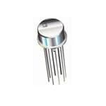
ICGOO电子元器件商城为您提供AD549LHZ由Analog设计生产,在icgoo商城现货销售,并且可以通过原厂、代理商等渠道进行代购。 AD549LHZ价格参考。AnalogAD549LHZ封装/规格:线性 - 放大器 - 仪表,运算放大器,缓冲器放大器, General Purpose Amplifier 1 Circuit TO-99-8。您可以下载AD549LHZ参考资料、Datasheet数据手册功能说明书,资料中有AD549LHZ 详细功能的应用电路图电压和使用方法及教程。
AD549LHZ是Analog Devices Inc.生产的一款高性能双极性输入运算放大器,具有极低的输入偏置电流和高输入阻抗,适用于对信号精度要求极高的应用场景。其典型应用包括精密仪器、医疗设备、高分辨率数据采集系统以及传感器信号调理电路。

在微弱信号放大方面,AD549LHZ常用于放大来自热电偶、光电二极管、应变计等传感器的微小电流或电压信号,尤其适合高阻抗源信号的处理。由于其低噪声和低失调特性,广泛应用于分析仪器如气相色谱仪、质谱仪等精密测量设备中。

此外,该器件也适用于电荷放大器电路,例如与压电传感器配合使用,在振动检测和超声波测量中发挥重要作用。在工业自动化和过程控制领域,AD549LHZ可用于高精度模拟前端设计,提升系统整体线性度与稳定性。

因其出色的直流精度和长期稳定性,AD549LHZ还常见于需要长期可靠运行的测试与测量设备中,如数字万用表、高精度ADC驱动电路等。总之,AD549LHZ是一款适用于高精度、低噪声、低漂移环境下的关键放大器元件,特别适合对信号完整性要求严苛的场合。
| 参数 | 数值 |
| -3db带宽 | - |
| 品牌 | Analog Devices |
| 产品目录 | 半导体 |
| 描述 | 精密放大器 IC ULTRALOW BIAS CURRENT |
| 产品分类 | 集成电路 - IC |
| 产品手册 | |
| 产品图片 |
|
| rohs | 符合RoHS |
| 产品系列 | 放大器 IC,精密放大器,Analog Devices AD549LHZ |
| 产品型号 | AD549LHZ |
| PCN设计/规格 | |
| 产品培训模块 | http://www.digikey.cn/PTM/IndividualPTM.page?site=cn&lang=zhs&ptm=30008http://www.digikey.cn/PTM/IndividualPTM.page?site=cn&lang=zhs&ptm=26202 |
| 产品目录页面 | |
| 产品种类 | 精密放大器 |
| 供应商器件封装 | TO-99-8 |
| 共模抑制比—最小值 | 90 dB |
| 关闭 | No |
| 包装 | 散装 |
| 压摆率 | 3 V/µs |
| 双重电源电压 | +/- 15 V |
| 商标 | Analog Devices |
| 增益带宽生成 | 1 MHz |
| 增益带宽积 | 1MHz |
| 安装类型 | 通孔 |
| 安装风格 | Through Hole |
| 封装 | Bulk |
| 封装/外壳 | TO-99-8 金属罐 |
| 封装/箱体 | TO-99-8 |
| 工作温度 | 0°C ~ 70°C |
| 工作电源电压 | 5 V to 18 V |
| 工厂包装数量 | 100 |
| 放大器类型 | 通用 |
| 最大功率耗散 | 500 mW |
| 最大双重电源电压 | +/- 18 V |
| 最大工作温度 | + 70 C |
| 最小双重电源电压 | +/- 5 V |
| 最小工作温度 | 0 C |
| 标准包装 | 1 |
| 电压-电源,单/双 (±) | ±5 V ~ 18 V |
| 电压-输入失调 | 300µV |
| 电压增益dB | 120 dB |
| 电流-电源 | 600µA |
| 电流-输入偏置 | 0.04pA |
| 电流-输出/通道 | 20mA |
| 电源电压-最大 | 18 V |
| 电源电压-最小 | 5 V |
| 电源电流 | 0.6 mA |
| 电源类型 | Dual |
| 电路数 | 1 |
| 系列 | AD549 |
| 视频文件 | http://www.digikey.cn/classic/video.aspx?PlayerID=1364138032001&width=640&height=505&videoID=2245193153001http://www.digikey.cn/classic/video.aspx?PlayerID=1364138032001&width=640&height=505&videoID=2245193159001 |
| 转换速度 | 3 V/us |
| 输入偏压电流—最大 | 2.8 pA |
| 输入电压范围—最大 | 10 V |
| 输入补偿电压 | 0.3 mV |
| 输出类型 | No |
| 通道数量 | 1 Channel |


- 商务部:美国ITC正式对集成电路等产品启动337调查
- 曝三星4nm工艺存在良率问题 高通将骁龙8 Gen1或转产台积电
- 太阳诱电将投资9.5亿元在常州建新厂生产MLCC 预计2023年完工
- 英特尔发布欧洲新工厂建设计划 深化IDM 2.0 战略
- 台积电先进制程称霸业界 有大客户加持明年业绩稳了
- 达到5530亿美元!SIA预计今年全球半导体销售额将创下新高
- 英特尔拟将自动驾驶子公司Mobileye上市 估值或超500亿美元
- 三星加码芯片和SET,合并消费电子和移动部门,撤换高东真等 CEO
- 三星电子宣布重大人事变动 还合并消费电子和移动部门
- 海关总署:前11个月进口集成电路产品价值2.52万亿元 增长14.8%


PDF Datasheet 数据手册内容提取
Ultralow Input Bias Current Operational Amplifier Data Sheet AD549 FEATURES CONNECTION DIAGRAM Ultralow input bias current GUARD PIN, CONNECTED 60 fA maximum (AD549L) TO CASE 100 fA maximum (AD549K) OFFSET NULL 8 V+ 1 AD549 7 250 fA maximum (AD549J) Input bias current guaranteed over the common-mode INVERINTPINUGT 2 6 OUTPUT voltage range Low offset voltage 3 5 NONINVERTING OFFSET 0.50 mV maximum (AD549K) INPUT 4 NULL 1.00 mV maximum (AD549J) V– Low offset drift 10kΩ 1 5 15 μV/°C maximum (AD549K) 4 –15V Lo27w00 p0 μo μVwA/°e Cmr maxaixmimumum su (AppDl5y4 c9uJr)r ent VOS TRIM 00511-001 Figure 1. Low input voltage noise 4 μV (typ) p-p over 0.1 Hz to 10 Hz MIL-STD-883B parts available APPLICATIONS Electrometer amplifier Photodiode preamp pH electrode buffer GENERAL DESCRIPTION connected to a point at the same potential as the input terminals, minimizing stray leakage to the case. The AD549 is available in The AD549 is a monolithic electrometer operational amplifier four performance grades. The J, K, and L versions are rated over with very low input bias current. Input offset voltage and input the commercial temperature range of 0°C to +70°C. The S grade offset voltage drift are laser trimmed for precision performance. is specified over the military temperature range of −55°C to +125°C The ultralow input current of the part is achieved with Topgate™ and is available processed to MIL-STD-883B, Rev. C. Extended JFET technology, a process development exclusive to Analog reliability plus screening is also available. Plus screening includes Devices, Inc. This technology allows fabrication of extremely 168 hour burn-in, as well as other environmental and physical low input current JFETs compatible with a standard junction tests derived from MIL-STD-883B, Rev. C. isolated bipolar process. The 1015 Ω common-mode impedance, which results from the bootstrapped input stage, ensures that PRODUCT HIGHLIGHTS the input current is essentially independent of the common- 1. The AD549 input currents are specified, 100% tested, and mode voltage. guaranteed after the device is warmed up. They are guaran- The AD549 is suited for applications requiring very low input teed over the entire common-mode input voltage range. current and low input offset voltage. It excels as a preamp for a 2. The AD549 input offset voltage and drift are laser trimmed wide variety of current output transducers, such as photodiodes, to 0.50 mV and 15 μV/°C (AD549K), and to 1 mV and photomultiplier tubes, or oxygen sensors. The AD549 can also 20 μV/°C (AD549J). be used as a precision integrator or low droop sample-and-hold. 3. A maximum quiescent supply current of 700 μA minimizes The AD549 is pin compatible with standard FET and electrometer heating effects on input current and offset voltage. op amps, allowing designers to upgrade the performance of present systems at little additional cost. 4. AC specifications include 1 MHz unity-gain bandwidth and 3 V/μs slew rate. Settling time for a 10 V input step is The AD549 is available in a TO-99 hermetic package. The case 5 μs to 0.01%. is connected to Pin 8, thus, the metal case can be independently Rev. K Document Feedback Information furnished by Analog Devices is believed to be accurate and reliable. However, no responsibility is assumed by Analog Devices for its use, nor for any infringements of patents or other One Technology Way, P.O. Box 9106, Norwood, MA 02062-9106, U.S.A. rights of third parties that may result from its use. Specifications subject to change without notice. No license is granted by implication or otherwise under any patent or patent rights of Analog Devices. Tel: 781.329.4700 ©2002–2015 Analog Devices, Inc. All rights reserved. Trademarks and registered trademarks are the property of their respective owners. Technical Support www.analog.com
AD549 Data Sheet TABLE OF CONTENTS Features .............................................................................................. 1 Offset Nulling ............................................................................. 11 Applications ....................................................................................... 1 AC Response with High Value Source and Feedback Connection Diagram ....................................................................... 1 Resistance .................................................................................... 12 General Description ......................................................................... 1 Common-Mode Input Voltage Overload ................................ 12 Product Highlights ........................................................................... 1 Differential Input Voltage Overload ........................................ 13 Revision History ............................................................................... 2 Input Protection ......................................................................... 13 Specifications ..................................................................................... 3 Sample-and-Difference Circuit to Measure Electrometer Leakage Currents ........................................................................ 13 Absolute Maximum Ratings ............................................................ 5 Photodiode Interface ................................................................. 14 ESD Caution .................................................................................. 5 Log Ratio Amplifier ................................................................... 15 Typical Performance Characteristics ............................................. 6 Temperature Compensated pH Probe Amplifier ................... 16 Functional Description .................................................................. 10 Outline Dimensions ....................................................................... 18 Minimizing Input Current ........................................................ 10 Ordering Guide .......................................................................... 18 Circuit Board Notes ................................................................... 10 REVISION HISTORY 2/15—Rev. J to Rev. K 7/07—Rev. F to Rev. G Updated Outline Dimensions ....................................................... 18 Changes to Figure 45 ...................................................................... 16 Changes to Temperature Compensated pH Probe 12/14—Rev. I to Rev. J Amplifier Section............................................................................ 17 Added L Model ................................................................... Universal Changes to Figure 46 ...................................................................... 17 Changes to Features Section and Applications Section ............... 1 Changes to Ordering Guide .......................................................... 18 Changes to Table 1 ............................................................................ 3 5/06—Rev. E to Rev. F Changes to Table 2 ............................................................................ 5 Changes to Log Ratio Amplifier Section ..................................... 15 Removed ESD Caution ..................................................................... 5 Changes to Temperature Compensated pH Probe 8/05—Rev. D to Rev. E Amplifier Section ............................................................................ 16 Change to Figure 22 .......................................................................... 9 Changes to Ordering Guide .......................................................... 18 5/04—Rev. C to Rev. D 6/14—Rev. H to Rev. I Updated Format .................................................................. Universal Deleted L Model............................................................. Throughout Changes to Features .......................................................................... 1 Change to Features Section ............................................................. 1 Updated Outline Dimensions ....................................................... 18 Changes to Input Offset Voltage Parameter and Input Voltage Added Ordering Guide .................................................................. 18 Noise Parameter, Table 1 .................................................................. 3 Changes to Ordering Guide .......................................................... 18 10/02—Rev. B to Rev. C 3/08—Rev. G to Rev. H Deleted Product Highlights #5 ........................................................ 1 Edits to Specifications ....................................................................... 3 Changes to Features .......................................................................... 1 Deleted Metallization Photograph .................................................. 3 Changes to Figure 1 .......................................................................... 1 Updated Outline Dimensions ....................................................... 13 Deleted Package Option Parameter ............................................... 4 Inserted ESD Caution ...................................................................... 5 7/02—Rev. A to Rev. B Changes to Figure 2, Figure 3, and Figure 7.................................. 6 Edits to Specifications ....................................................................... 2 Changes to Figure 11 ........................................................................ 7 Changes to Figure 17 ........................................................................ 8 Changes to Figure 41 ...................................................................... 14 Rev. K | Page 2 of 18
Data Sheet AD549 SPECIFICATIONS At 25°C and V = ±15 V dc, unless otherwise noted; all minimum and maximum specifications are guaranteed; specifications in boldface S are tested on all production units at final electrical test, and results from those tests are used to calculate outgoing quality levels. Table 1. AD549J AD549K AD549L AD549S Parameter Min Typ Max Min Typ Max Min Typ Max Min Typ Max Unit INPUT BIAS CURRENT1 Either Input, V = 0 V 150 250 75 100 40 60 75 100 fA CM Either Input, V = ±10 V 150 250 75 100 40 60 75 100 fA CM Either Input at T , 11 4.2 2.8 420 pA MAX V = 0 V CM Offset Current 50 30 20 30 fA Offset Current at T 2.2 1.3 0.85 125 pA MAX INPUT OFFSET VOLTAGE2 Initial Offset 0.5 1.0 0.15 0. 5 0.3 0.5 0.3 0.5 mV Offset at T 1.9 0.9 0.9 2.0 mV MAX vs. Temperature 10 20 10 15 5 10 10 15 μV/°C vs. Supply 32 100 10 32 10 32 10 32 μV/V vs. Supply, T to T 32 100 10 32 10 32 32 50 μV/V MIN MAX Long-Term Offset Stability 15 15 15 15 μV/month INPUT VOLTAGE NOISE f = 0.1 Hz to 10 Hz 4 4 6 4 4 μV p-p f = 10 Hz 90 90 90 90 nV/√Hz f = 100 Hz 60 60 60 60 nV/√Hz f = 1 kHz 35 35 35 35 nV/√Hz f = 10 kHz 35 35 35 35 nV/√Hz INPUT CURRENT NOISE f = 0.1 Hz to 10 Hz 0.7 0.5 0.36 0.5 fA rms f = 1 kHz 0.22 0.16 0.11 0.16 fA/√Hz INPUT IMPEDANCE Differential V = ±1 1013||1 1013||1 1013||1 1013||1 Ω||pF DIFF Common Mode V = ±10 V 1015||0.8 1015||0.8 1015||0.8 1015||0.8 Ω||pF CM OPEN-LOOP GAIN V at ±10 V, R = 10 kΩ 300 1000 300 1000 300 1000 300 1000 V/mV OUT L V at ±10 V, R = 10 kΩ, 300 800 300 800 300 800 300 800 V/mV OUT L T to T MIN MAX V = ±10 V, R = 2 kΩ 100 250 100 250 100 250 100 250 V/mV OUT L V = ±10 V, R = 2 kΩ, 80 200 80 200 80 200 25 150 V/mV OUT L T to T MIN MAX INPUT VOLTAGE RANGE Differential3 ±20 ±20 ±20 ±20 V Common-Mode Voltage −10 +10 −10 +10 −10 +10 −10 +10 V Common-Mode Rejection Ratio −10 V ≤ V ≤ +10 V 80 90 90 100 90 100 90 100 dB CM T to T 76 80 80 90 80 90 80 90 dB MIN MAX OUTPUT CHARACTERISTICS V at R = 10 kΩ, T to −12 +12 −12 +12 −12 +12 −12 +12 V OUT L MIN T MAX V at R = 2 kΩ, T to T −10 +10 −10 +10 −10 +10 −10 +10 V OUT L MIN MAX Short-Circuit Current 15 20 35 15 20 35 15 20 35 15 20 35 mA T to T 9 9 9 6 mA MIN MAX Load Capacitance Stability, 4000 4000 4000 4000 pF G = +1 Rev. K | Page 3 of 18
AD549 Data Sheet AD549J AD549K AD549L AD549S Parameter Min Typ Max Min Typ Max Min Typ Max Min Typ Max Unit FREQUENCY RESPONSE Unity Gain, Small Signal 0.7 1.0 0.7 1.0 0.7 1.0 0.7 1.0 MHz Full Power Response 50 50 50 50 kHz Slew Rate 2 3 2 3 2 3 2 3 V/μs Settling Time, 0.1% 4.5 4.5 4.5 4.5 μs Settling Time, 0.01% 5 5 5 5 μs Overload Recovery, 50% 2 2 2 2 μs Overdrive, G = −1 POWER SUPPLY Rated Performance ±15 ±15 ±15 ±15 V Operating ±5 ±18 ±5 ±18 ±5 ±18 ±5 ±18 V Quiescent Current 0.60 0.70 0.60 0.70 0.60 0.70 0.60 0.70 mA TEMPERATURE RANGE Operating, Rated 0 70 0 70 0 70 −55 +125 °C Performance Storage −65 +150 −65 +150 −65 +150 −65 +150 °C 1 Bias current specifications are guaranteed after five minutes of operation at TA = 25°C. Bias current increases by a factor of 2.3 for every 10°C rise in temperature. 2 Input offset voltage specifications are guaranteed after five minutes of operation at TA = 25°C. 3 Defined as maximum continuous voltage between the inputs, such that neither input exceeds ±10 V from ground. Rev. K | Page 4 of 18
Data Sheet AD549 ABSOLUTE MAXIMUM RATINGS Table 2. Stresses at or above those listed under Absolute Maximum Parameter Rating Ratings may cause permanent damage to the product. This is a Supply Voltage ±18 V stress rating only; functional operation of the product at these Internal Power Dissipation 500 mW or any other conditions above those indicated in the operational Input Voltage1 ±18 V section of this specification is not implied. Operation beyond Output Short-Circuit Duration Indefinite the maximum operating conditions for extended periods may Differential Input Voltage +V and −V affect product reliability. S S Storage Temperature Range −65°C to +125°C Operating Temperature Range ESD CAUTION AD549J, AD549K, AD549L 0°C to +70°C AD549S −55°C to +125°C Lead Temperature (Soldering, 60 sec) 300°C 1 For supply voltages less than ±18 V, the absolute maximum input voltage is equal to the supply voltage. Rev. K | Page 5 of 18
AD549 Data Sheet TYPICAL PERFORMANCE CHARACTERISTICS 20 800 A) µ T ( 15 N 700 E V) RR UT VOLTAGE ( 10 VIN+ UIESCENT CU 600 NP VIN– R Q I E 5 FI 500 LI P M 0 00511-002 A 400 00511-005 0 5 10 15 20 0 5 10 15 20 SUPPLY VOLTAGE (±V) SUPPLY VOLTAGE (±V) Figure 2. Input Voltage Range vs. Supply Voltage Figure 5. Quiescent Current vs. Supply Voltage 20 120 25°C RL = 10kΩ +VOUT dB) G (V) 15 ATIO ( 110 WIN –VOUT N R AGE S 10 JECTIO 100 T E L R T VO ODE 90 UTPU 5 ON-M O M 80 M 0 00511-003 CO 70 00511-006 0 5 10 15 20 –20 –10 0 10 20 SUPPLY VOLTAGE (±V) INPUT COMMON-MODE VOLTAGE (V) Figure 3. Output Voltage Swing vs. Supply Voltage Figure 6. CMRR vs. Input Common-Mode Voltage 30 3000 VS = ±15V p) 25 p- NG (V 20 V/mV)1000 WI N ( TAGE S 15 OP GAI L O O L T V 10 EN- 300 U P P O T U O 5 0 00511-004 100 00511-007 10 100 1k 10k 100k 0 5 10 15 20 LOAD RESISTANCE (Ω) SUPPLY VOLTAGE (±V) Figure 4. Output Voltage Swing vs. Load Resistance Figure 7. Open-Loop Gain vs. Supply Voltage Rev. K | Page 6 of 18
Data Sheet AD549 3000 50 45 V) AIN (V/m1000 ENT (fA) 40 N-LOOP G 300 PUT CURR 3350 E N P I O 25 100 00511-008 20 00511-011 –55 –25 5 35 65 95 125 0 5 10 15 20 TEMPERATURE (°C) POWER SUPPLY VOLTAGE (±V) Figure 8. Open-Loop Gain vs. Temperature Figure 11. Input Bias Current vs. Power Supply Voltage 30 160 25 Hz) 140 V/ n 120 20 Y ( T V) NSI 100 µ E ∆IVI (OS 15 TRAL D 80 C 10 E SP 60 E S 5 OI 0 00511-009 N 4200 00511-012 0 1 2 3 4 5 6 7 10 100 1k 10k WARM-UP TIME (Minutes) FREQUENCY (Hz) Figure 9. Change in Offset Voltage vs. Warm-Up Time Figure 12. Input Voltage Noise Spectral Density 50 100k WHENEVER JOHNSON NOISE IS GREATER THAN AMPLIFIER NOISE, AMPLIFIER NOISE CAN BE CONSIDERED NEGLIGIBLE FOR THE APPLICATION 45 10k p-p) 1kHz BANDWIDTH T (fA) 40 GE (µV 1k JOHRNESSOISNT NOORISE N A E T RR 35 OL 100 U V T C SE INPU 30 T NOI 10 U 10Hz BANDWIDTH P N 25 I 1 20 00511-010 0.1 AMPLIFIER GENERATED NOISE 00511-013 –10 –5 0 5 10 100k 1M 10M 100M 1G 10G 100G COMMON-MODE VOLTAGE (V) SOURCE RESISTANCE (Ω) Figure 10. Input Bias Current vs. Common-Mode Voltage Figure 13. Noise vs. Source Resistance Rev. K | Page 7 of 18
AD549 Data Sheet 100 100 120 80 80 dB) 100 O ( N (dB)60 60 egrees) ON RATI 80 +PSSR P GAI40 40 GIN (D JECTI 60 LOO20 20 MAR Y RE 40 OEPN- 0 0 HASE SUPPL 20 –PSSR P R E –20 –20 W 0 –40 –40 00511-014 PO –20 00511-017 10 100 1k 10k 100k 1M 10M 10 100 1k 10k 100k 1M 10M FREQUENCY (Hz) FREQUENCY (Hz) Figure 14. Open-Loop Frequency Response Figure 17. PSRR vs. Frequency Response 40 10 35 G (V) 30 G (V) 5 10mV N N 5mV WI 25 WI S S 1mV E E G G A 20 A 0 T T L L O O T V 15 T V 10mV U U P P 5mV UT 10 UT –5 O O 1mV 50 00511-015 –10 00511-018 10 100 1k 10k 100k 1M 0 1 2 3 4 5 FREQUENCY (Hz) SETTLING TIME (µs) Figure 15. Large Signal Frequency Response Figure 18. Output Voltage Swing and Error vs. Settling Time 100 B) O (d 80 TI A R N 60 O TI C JE 40 E R E D O 20 M N- O M M 0 CO –20 00511-016 10 100 1k 10k 100k 1M 10M FREQUENCY (Hz) Figure 16. CMRR vs. Frequency Rev. K | Page 8 of 18
Data Sheet AD549 +VS 10kΩ 0.1µF +VS 0.1µF 2 7 10kΩ VIN 2 7 AD549 5 VOUT VIN 3 4 0.1µF R10LkΩ C10L0pF ISWNQAPUUVAETRE AD549 5 RL CL VOUT 3 4 0.1µF 10kΩ 100pF ISWNQAPUUVAETRE –VS 00511-019 –VS 00511-022 Figure 19. Unity-Gain Follower Figure 22. Unity-Gain Inverter 5V 5V 5µs 00511-020 5µs 00511-023 Figure 20. Unity-Gain Follower Large Signal Pulse Response Figure 23. Unity-Gain Inverter Large Signal Pulse Response 10mV 10mV 1µs 00511-021 1µs 00511-024 Figure 21. Unity-Gain Follower Small Signal Pulse Response Figure 24. Unity-Gain Inverter Small Signal Pulse Response Rev. K | Page 9 of 18
AD549 Data Sheet FUNCTIONAL DESCRIPTION MINIMIZING INPUT CURRENT CIRCUIT BOARD NOTES The AD549 is optimized for low input current and offset A number of physical phenomena generate spurious currents voltage. Careful attention to how the amplifier is used reduces that degrade the accuracy of low current measurements. Figure 27 input currents in actual applications. is a schematic of a current to voltage (I-to-V) converter with these parasitic currents modeled. Keep the amplifier operating temperature as low as possible to minimize input current. Like other JFET input amplifiers, the CF AD549 input current is sensitive to chip temperature, rising by a factor of 2.3 for every 10°C. Figure 25 is a plot of the AD549 RF 2 input current vs. ambient temperature. AD549 6 + 1nA VOUT fS 3 8 – 100pA T AS CURREN 101ppAA VRSP CP II' =RVP+ddCTPV +ddVTCP 00511-027 BI Figure 27. Sources of Parasitic Leakage Currents T PU 100fA N Finite resistance from input lines to voltages on the board, I modeled by Resistor R , results in parasitic leakage. Insulation 10fA P 1fA 00511-025 rthesei satmanpcleif ioefr msiognrea lt haannd 1s0u1p5 pΩly m linuests btoe cmaapiintataliiznee odn b tehtwe eloewn –55 –25 5 35 65 95 125 input currents of the AD549. Standard PCB material does not TEMPERATURE (°C) have high enough insulation resistance; therefore, connect the Figure 25. Input Bias Current vs. Ambient Temperature input leads of the AD549 to standoffs made of insulating On-chip power dissipation raises the chip operating tempera- material with adequate volume resistivity (that is, Teflon®). The ture, causing an increase in input bias current. Due to the low surface of the insulator must be kept clean to preserve surface quiescent supply current of the AD549, the chip temperature resistivity. For Teflon, an effective cleaning procedure consists is less than 3°C higher than its ambient temperature when the of swabbing the surface with high grade isopropyl alcohol, (unloaded) amplifier is operating with 15 V supplies. The rinsing with deionized water, and baking the board at 80°C for difference in the input current is negligible. 10 minutes. However, heavy output loads can cause a significant increase in In addition to high volume and surface resistivity, other proper- chip temperature and a corresponding increase in the input ties are desirable in the insulating material chosen. Resistance current. Maintaining a minimum load resistance of 10 Ω is to water absorption is important because surface water films recommended. Input current vs. additional power dissipation drastically reduce surface resistivity. The insulator chosen due to output drive current is plotted in Figure 26. should also exhibit minimal piezoelectric effects (charge 6 emission due to mechanical stress) and triboelectric effects (charge generated by friction). Charge imbalances generated T by these mechanisms can appear as parasitic leakage currents. EN 5 RR These effects are modeled by Variable Capacitor CP in Figure 27. CU Table 3 lists various insulators and their properties.2 S A 4 BI Guarding the input lines by completely surrounding them with T BASED ON PU TYPICAL IB = 40fA a metal conductor biased near the potential of the input lines N D I 3 has two major benefits. First, parasitic leakage from the signal E LIZ line is reduced because the voltage between the input line and A M the guard is very low. Second, stray capacitance at the input R 2 NO 1 00511-026 nsiogdnea li sb amnidnwimiditzhe da.n Idn pthuet cstaapbaicliittya nocf et hcea nI -stuob-Vst acnotniavlelryt edre. g rade 0 25 50 75 100 125 150 175 200 ADDITIONAL INTERNAL POWER DISSIPATION (mW) 2 Electronic Measurements, pp. 15–17, Keithley Instruments, Inc., Cleveland, Ohio, 1977. Figure 26. Input Bias Current vs. Additional Power Dissipation Rev. K | Page 10 of 18
Data Sheet AD549 The case of the AD549 is connected to Pin 8 so that it can be OFFSET NULLING bootstrapped near the input potential. This minimizes pin The AD549 input offset voltage can be nulled by using balance leakage and input common-mode capacitance due to the case. Pin 1 and Pin 5, as shown in Figure 30. Nulling the input offset Guard schemes for inverting and noninverting amplifier voltage in this fashion introduces an added input offset voltage topologies are illustrated in Figure 28 and Figure 29. drift component of 2.4 μV/°C per mV of nulled offset (a maximum CF additional drift of 1.2 μV/°C for the AD549K and AD549L, and GUARD 2.4 μV/°C for the AD549J). RF +VS 2 AD549 6 + VOUT 2 7 IN 3 8 – AD549 6 + 00511-028 3 4 1 5 VOUT– Figure 28. Inverting Amplifier with Guard 10kΩ –VS 00511-030 Figure 30. Standard Offset Null Circuit GUARD The approach in Figure 31 can be used when the amplifier is 3 VOUT used as an inverter. This method introduces a small voltage + AD549 6 + referenced to the power supplies in series with the positive VS 2 8 RF input terminal of the amplifier. The amplifier input offset – voltage drift with temperature is not affected. However, variation of the power supply voltages causes offset shifts. R–I 00511-029 RI 2 RF Figure 29. Noninverting Amplifier with Guard + AD549 6 + Other guidelines include keeping the circuit layout as compact VI 3 VOUT– as possible and keeping the input lines short. Keeping the assembly – +VS rigid and minimizing sources of vibration reduces triboelectric 499kΩ 499kΩ 100kΩ and piezoelectric effects. All precision, high impedance circuitry roerq turiiraexsi ashl icealbdliensg faogra rinemst ointtee crfoenrenneccet inooniss et.o U tshee lionwp unto siisgen caol alxiniaels . 200Ω 0.1µF –VS 00511-031 Figure 31. Alternate Offset Null Circuit for Inverter Table 3. Insulating Materials and Characteristics Volume Resistivity Minimal Minimal Resistance to Material (V to CM) Triboelectric Effect1 Piezoelectric Effect1 Water Absorption1 Teflon 1017 to 1018 W W G Kel-F® 1017 to 1018 W M G Sapphire 1016 to 1018 M G G Polyethylene 1014 to 1018 M G M Polystyrene 1012 to 1018 W M M Ceramic 1012 to 1014 W M W Glass Epoxy 1010 to 1017 W M W PVC 1010 to 1015 G M G Phenolic 105 to 1012 W G W 1 G: good with regard to property; M: moderate with regard to property; W: weak with regard to property. Rev. K | Page 11 of 18
AD549 Data Sheet AC RESPONSE WITH HIGH VALUE SOURCE AND In an inverting configuration, the differential input capacitance FEEDBACK RESISTANCE forms a pole in the loop transmission of the circuit. This can create peaking in the ac response and possible instability. A Source and feedback resistances greater than 100 kΩ magnify feedback capacitance can be used to stabilize the circuit. The the effect of the input capacitances (stray and inherent to inverter pulse response with R and R equal to 1 MΩ appears the AD549) on the ac behavior of the circuit. The effects of F S in Figure 34. Figure 35 shows the response of the same circuit common-mode and differential input capacitances should be with a 1 pF feedback capacitance. Typical differential input taken into account because the circuit bandwidth and stability capacitance for the AD549 is 1 pF. can be adversely affected. 10mV 5µs 10mV 5µs 00511-032 Figure 34. Inverter Pulse Response with 1 MΩ Source 00511-034 Figure 32. Follower Pulse Response from 1 MΩ Source Resistance, and Feedback Resistance Case Not Bootstrapped 10mV 5µs 10mV 5µs 00511-033 Figure 35. Inverter Pulse Response with 1 MΩ Source 00511-035 Figure 33. Follower Pulse Response from 1 MΩ Source Resistance, and Feedback Resistance, 1 pF Feedback Capacitance Case Bootstrapped COMMON-MODE INPUT VOLTAGE OVERLOAD In a follower, the source resistance and input common-mode capacitance form a pole that limits the bandwidth to ½πRC. The rated common-mode input voltage range of the AD549 is S S Bootstrapping the metal case by connecting Pin 8 to the output from 3 V less than the positive supply voltage to 5 V greater than minimizes capacitance due to the package. Figure 32 and the negative supply voltage. Exceeding this range degrades the Figure 33 show the follower pulse response from a 1 MΩ source CMRR of the amplifier. Driving the common-mode voltage above resistance with and without the package connected to the the positive supply causes the amplifier output to saturate at the output. Typical common-mode input capacitance for the upper limit of the output voltage. Recovery time is typically 2 μs AD549 is 0.8 pF. after the input has been returned to within the normal operating range. Driving the input common-mode voltage within 1 V of the negative supply causes phase reversal of the output signal. In this case, normal operation typically resumes within 0.5 μs of the input voltage returning within range. Rev. K | Page 12 of 18
Data Sheet AD549 DIFFERENTIAL INPUT VOLTAGE OVERLOAD RPROTECT A plot of the AD549 input currents vs. differential input SOURCE 3 voltage (defined as VIN+ − VIN−) appears in Figure 36. The AD549 6 input current at either terminal stays below a few hundred fteom 1t.5o aVm apbso uvne ttihl eo noeth ienrp tuetr tmerimnailn. aUl nisd feorr tcheeds eh icgohnedr itthioanns ,1 t Vhe 2 00511-038 Figure 38. Follower with Input Current Limit input current limits at 30 μA. Figure 39 is a schematic of the AD549 as an inverter with an 100µ input voltage clamp. Bootstrapping the clamp diodes at the 10µ IIN– IIN+ inverting input minimizes the voltage across the clamps and 1µ keeps the leakage due to the diodes low. Use low leakage diodes, 100n such as the FD333s, and shield them from light to prevent photo- A) NT ( 10n currents from being generated. Even with these precautions, the RE diodes measurably increase input current and capacitance. R 1n U C UT 100p RF P N 10p SOURCE 2 I 1p AD549 6 10100ff–5 –4 –3 –2 –1 0 1 2 3 4 5 00511-036 PDRIOOTDEECST 3 00511-039 Figure 39. Input Voltage Clamp with Diodes DIFFERENTIAL INPUT VOLTAGE (V) (VIN+ – VIN–) SAMPLE-AND-DIFFERENCE CIRCUIT TO MEASURE Figure 36. Input Current vs. Differential Input Voltage ELECTROMETER LEAKAGE CURRENTS INPUT PROTECTION There are a number of methods used to test electrometer leakage The AD549 safely handles any input voltage within the supply currents, including current integration and direct I-to-V con- voltage range. Subjecting the input terminals to voltages beyond version. Regardless of the method used, board and interconnect the power supply can destroy the device or cause shifts in input cleanliness, proper choice of insulating materials (such as Teflon current or offset voltage if the amplifier is not protected. or Kel-F), correct guarding and shielding techniques, and care A protection scheme for the amplifier as an inverter is shown in physical layout are essential to making accurate leakage in Figure 37. RP is chosen to limit the current through the measurements. inverting input to 1 mA for expected transient (less than 1 sec) Figure 40 is a schematic of the sample-and-difference circuit. It overvoltage conditions, or to 100 μA for a continuous overload. uses two AD549 electrometer amplifiers (A and B) as I-to-V Because R is inside the feedback loop and is much lower in P converters with high value (1010 Ω) sense resistors (RSa and value than the amplifier input resistance, it does not affect the RSb). R1 and R2 provide for an overall circuit sensitivity of dc gain of the inverter. However, the Johnson noise of the 10 fA/mV (10 pA full scale). C and C provide noise suppression resistor adds root sum of squares to the amplifier input noise. C F and loop compensation. C should be a low leakage polystyrene C RF capacitor. An ultralow leakage Kel-F test socket is used for con- RPROTECT CF tacting the device under test. Rigid Teflon coaxial cable is used to make connections to all high impedance nodes. The use of SOURCE 2 rigid coaxial cable affords immunity to error induced by mechan- AD549 6 ical vibration and provides an outer conductor for shielding. The 3 00511-037 entire circuit is enclosed in a grounded metal box. Figure 37. Inverter with Input Current Limit In the corresponding version of this scheme for a follower, shown in Figure 38, R and the capacitance at the positive input P terminal produce a pole in the signal frequency response at a f = ½πRC. Again, the Johnson noise, R , adds to the input P voltage noise of the amplifier. Rev. K | Page 13 of 18
AD549 Data Sheet The test apparatus is calibrated without a device under test Although a series of devices can be tested after only one calibra- present. After power is turned on, a 5 minute stabilization tion measurement, calibration should be updated periodically period is required. First, V and V are measured. These to compensate for any thermal drift of the I-to-V converters or ERR1 ERR2 voltages are the errors caused by the offset voltages and leakage changes in the ambient environment. Laboratory results have currents of the I-to-V converters. shown that repeatable measurements within 10 fA can be realized when this apparatus is properly implemented. These results are V = 10 (V A – I A × RSa) ERR1 OS B achieved in part by the design of the circuit, which eliminates V = 10 (V B – I B × RSb) ERR2 OS B relays and other parasitic leakage paths in the high impedance CC CF signal lines, and in part by the inherent cancellation of errors 20pF 0.1µF through the calibration and measurement procedure. RSa R2 PHOTODIODE INTERFACE 1010Ω 9.01kΩ R1 The low input current and low input offset voltage of the AD549 1kΩ make it an excellent choice for very sensitive photodiode preamps 2 (see Figure 41). The photodiode develops a signal current, I, S A CAL/TEST AD549 6 + equal to VERR1/VA 3 8 – IS = R × P GUARD where P is light power incident on the diode surface, in watts, I (+) and R is the photodiode responsivity in amps/watt. R converts F – DEVICE VOUT the signal current to an output voltage VOS UNDER – + TEST R2 CF V = R × I 9.01kΩ 0.1µF OUT F S I (–) RF 1kRΩ1 VERR2/VB 109Ω 3 8 ADB549 6 + 10CpFF 2 2 IS AD549 6 10kΩ + 5 2C0pCF 0.C1µFF 3 1 1µF VOUT 4 – 1R0S10bΩ 9.0R12kΩ –VS 00511-041 R1k1Ω 00511-040 The dc error sourceFsi gaunrde 4a1n. Pehqoutoivdaioldene tP rceiarmcupi t for a small area Figure 40. Sample and Difference Circuit for Measuring (0.2 mm square) photodiode are indicated in Figure 42. Electrometer Leakage Currents Once measured, these errors are subtracted from the readings 10R9FΩ taken with a device under test present. Amplifier B closes the feedback loop to the device under testing in addition to pro- CF viding the I-to-V conversion. The offset error of the device 10pF uafnfedcetr tthees ttiensgt ampepaesaurrse ams ean cto. mAsm ao rne-smulot,d oen sliyg tnhael laenadk adgoee s not IS 10R9ΩS 20CpFS IS– A VOUT+ current of the device under testing is measured. – VOS + – 00511-042 VA – VERR1 = 10[RSa × IB(+)] Figure 42. Photodiode Preamp DC Error Sources V – V = 10[RSb × I (–)] X ERR2 B Rev. K | Page 14 of 18
Data Sheet AD549 Input current, I , contributes an output voltage error, V , gain that multiplies the op amp input voltage noise contribu- B E1 proportional to the feedback resistance tion. A single-pole filter at the output of the amplifier limits the op amp output voltage noise bandwidth to 26 Hz, comparable V = I × R E1 B F to the signal bandwidth. This greatly improves the signal-to- The input voltage offset of the op amp causes an error current noise ratio of the preamplifier (in this case, by a factor of 3). through the photodiode shunt resistance, R S 10µ I = V /R IF AND CS, NO FILTERS OS S aTmhep leVirfEire2o r=r o c(uu1tr p+rue Rnt Fte/ qrReuSs)auVl lttOosS in an error voltage (VE2) at the TRIBUTIONSSITY (nV/ Hz) 1µ IF AND OCPSE, NW-AILTDOH5O 4F9PIL GTAEIRNS NN OE Given typical values of photodiode shunt resistance (on the order CD E L ofefe 1d0b9a Ωck) ,r ResFi/sRtaS nccaen iesa ussileyd b. eA glsroe,a RteFr/ RthS ainn c1r,e easspese cwiaitllhy tief ma plaerrgae- E NOISECTRA100n GP ture because photodiode shunt resistance typically drops by a LTASE S EN CONTRIBUTION, flToahwcet o oArf fDosef5 t2 4v 9fooKltra oegfvef eearrnysd a1 l 0og°wuCa d rrraiisnfett emienud ts emtm baepx euimrsaeutdum troe 0 .m .A5a0ni n motpaVi an mo afcpfcs weutri tahc y. VONOI 10n ECWNOITNHT RFIILBTUETRION, NO FILTER 00511-044 1 10 100 1k 10k 100k 1M voltage and 15 mV/°C drift for very sensitive applications. FREQUENCY (Hz) Photodiode Preamp Noise Figure 44. Spectral Density of the Photodiode Preamp Noise Sources vs. Frequency Noise limits the signal resolution obtainable with the preamp. LOG RATIO AMPLIFIER The output voltage noise divided by the feedback resistance is the minimum current signal that can be detected. This mini- Logarithmic ratio circuits are useful for processing signals with mum detectable current divided by the responsivity of the wide dynamic range. The 60 fA maximum input current of the photodiode represents the lowest light power that is detectable AD549L makes it possible to build a log ratio amplifier with by the preamp. 1% log conformance for input currents ranging from 10 pA to Noise sources associated with the photodiode, amplifier, and 1 mA, a dynamic range of 160 dB. feedback resistance are shown in Figure 43; Figure 44 is the The log ratio amplifier in Figure 45 provides an output voltage spectral density vs. frequency plot of the contribution of each of proportional to the log base 10 of the ratio of Input Current I 1 the noise sources to the output voltage noise (circuit parameters and Input Current I. Resistor R1 and Resistor R2 are provided 2 in Figure 42 are assumed). The rms contribution of each noise for voltage inputs. Because NPN devices are used in the feedback source to the total output voltage noise is obtained by loop of the front-end amplifiers that provide the log transfer integrating the square of its spectral density function over function, the output is valid only for positive input voltages and frequency. The rms value of the output voltage noise is the input currents. The input currents set the Collector Current IC1 square root of the sum of all contributions. Minimizing the total and Collector Current IC2 of a matched pair of log transistors, area under these curves optimizes the resolution of the Q1 and Q2, to develop Voltage V and Voltage V A B preamplifier for a given bandwidth. V , V = –(kT/q)ln IC/IES A B IF where IES is the saturation current of the transistor. RF The difference of VA and VB is taken by the subtractor section to CF obtain V = (kT/q)ln(IC2/IC1) C IS RS CS IN A V is scaled up by the ratio of (R9 + R10)/R8, which is equal to C EN 00511-043 avpopltraogxei m ately 16 at room temperature, resulting in the output Figure 43. Photodiode Preamp Noise Sources V = 1 V × log(IC2/IC1) OUT The photodiode preamp in Figure 41 can detect a signal current of 26 fA rms at a bandwidth of 16 Hz, which, assuming a R8 is a resistor with a positive 3500 ppm/°C temperature coeffi- photodiode responsivity of 0.5 A/W, translates to a 52 fW rms cient to provide the necessary temperature compensation. The minimum detectable power. The photodiode used has a high parallel combination of R15 and R7 is provided to keep the gain source resistance and low junction capacitance. C sets the of the subtractor section for positive and negative inputs matched F signal bandwidth with R and also limits the peak in the noise over temperature. F Rev. K | Page 15 of 18
AD549 Data Sheet Frequency compensation is provided by R11, R12, C1, and C2. composed of R13, D1, R16, R14, D2, and R17 compensate for The bandwidth of the circuit is 300 kHz at input signals greater these errors, so that this circuit has less than a 1% log confor- than 50 μA; bandwidth decreases smoothly with decreasing mance error at 1 mA input currents. The correct value for R13 signal levels. and R14 depends on the type of log transistors used. The 49.9 kΩ resistors were chosen for use with LM394 transistors. Smaller To trim the circuit, set the input currents to 10 μA and trim the resistance values are needed for smaller log transistors. A3 offset using the trim potentiometer of the amplifier for the output to equal 0. Next, set I to 1 μA and adjust the output to TEMPERATURE COMPENSATED pH PROBE 1 equal 1 V by trimming R10. Additional offset trims on Ampli- AMPLIFIER fier A1 and Amplifier A2 can be used to increase the voltage A pH probe can be modeled as an mV-level voltage source input accuracy and dynamic range. with a series source resistance dependent on the electrode The very low input current of the AD549 makes this circuit composition and configuration. The glass bulb resistance of a useful over a very wide range of signal currents. The total input typical pH electrode pair falls between 106 Ω and 109 Ω. It is current (which determines the low level accuracy of the circuit) therefore important to select an amplifier with low enough is the sum of the amplifier input current, the leakage across the input currents such that the voltage drop produced by the compensating capacitor (negligible if a polystyrene or Teflon amplifier input bias current and the electrode resistance does capacitor is used), and the collector-to-collector and collector- not become an appreciable percentage of a pH unit. to-base leakages of one side of the dual log transistors. The The circuit in Figure 46 illustrates the use of the AD549 as a pH magnitudes of these last two leakages depend on the amplifier probe amplifier. As with other electrometer applications, the use of input offset voltage and are typically less than 10 fA with 1 mV guarding, shielding, and Teflon standoffs is necessary to capitalize offsets. The low level accuracy is limited primarily by the on the AD549 low input current. If an AD549L (60 fA maximum amplifier input current, only 60 fA maximum when the input current) is used, the error contributed by the input current is AD549L is used. held below 60 μV for pH electrode source impedances up to 109 Ω. The effects of the emitter resistance of Q1 and Q2 can degrade Input offset voltages (which can be trimmed) are below 0.5 mV. circuit accuracy at input currents above 100 μA. The networks FOR EACH AMPLIFIER 10kΩ PIN 7 +VS 4 V1 0.1µF 3 1 OFFSET 0.1µF ADA5149 5 6 D3 PIN 4 –VS Q1, Q2 = LM394 I1 IN 2 DUAL LOG TRANSISTORS 10C01pF R4.1919kΩ 1Rk1Ω5 R1 * V1 IN 10kΩ Q1 A 20Rk3Ω 20Rk5Ω 15Rk7Ω R16 R14 10Ω 3 49.9kΩ D1 A3 VOUT AD549 6 D2 5 SCALE R101Ω7 R491.39kΩ 2 4 1 10kΩ 2Rk1Ω0 FAADCJTOR OUTPUT OFFSET R2 10kΩ V2 IN C2 Q2 B 20Rk4Ω 20Rk6Ω * R1k8Ω 14R.39kΩ 100pF 4.99kΩ VOUT = 1V ×LOG10 VV21 I2 IN 2 A2 D4 VOUT = 1V ×LOG10 II21 AD549 5 6 DR81,, RD145 1 1Nk4Ω14 +8 3D5I0O pDpEmS/°C TC RESISTOR *TELLAB QB1 OR PRECISION RESISTOR PT146 3 1 ALL OTHER RESISTORS ARE 1% METAL FILM 4 VO12F0FkSΩET 00511-045 Figure 45. Log Ratio Amplifier Rev. K | Page 16 of 18
Data Sheet AD549 The pH probe output is ideally 0 V at a pH of 7, independent the compensation. The AD549 is set for a noninverting gain of of temperature. The slope of the transfer function of the probe, 13.51. The output of the AD590 circuitry (Point C) is equal to though predictable, is temperature dependent (−54.2 mV/pH at 10 V at 100°C and decreases by 26.8 mV/°C. The output of the 0°C and −74.04 mV/pH at 100°C). By using an AD590 tempera- AD534 analog divider (Point D) is a temperature-compensated ture sensor and an AD534 analog divider, an accurate temperature output voltage centered at 0 V for a pH of 7 and has a transfer compensation network can be added to the basic pH probe ampli- function of –1.00 V/pH unit. The output range spans from fier. Table 4 shows voltages at various points, thereby illustrating −7.00 V (pH = 14) to +7.00 V (pH = 0). +15V 0.1µF 0.1µF 14 pH (A) PROBE 3 7 AD534 OUTPUT (B) (D) AD549 6 10 Z2 OUT 12 OUTPUT 2 4 8 0.1µF 11 Z1 (C) Y2 7 1 X1 12kΩ 2 X2 Y1 6 8 1kΩ 1kΩ 0.1µF SCALE FACTOR ADJUST +15V –15V AD590 + IN STAINLESS STEEL PROBE OR AC2626 – 26.6kΩ 00511-046 Figure 46. Temperature Compensated pH Amplifier Table 4. Illustration of Temperature Compensation Point Probe Temperature (°C) A (Probe Output) (mV) B (A × 13.51) (V) C (AD590 Output) (V) D (10 × (B ÷ C)) (V) 0 54.20 0.732 7.32 1.00 25 59.16 0.799 7.99 1.00 37 61.54 0.831 8.31 1.00 60 66.10 0.893 8.93 1.00 100 74.04 1.000 10.00 1.00 Rev. K | Page 17 of 18
AD549 Data Sheet OUTLINE DIMENSIONS REFERENCE PLANE 0.50(12.70) MIN 0.100 (2.54) 0.185 (4.70) 0.250 (6.35) MIN BSC 0.165 (4.19) 0.050 (1.27) MAX 0.160 (4.06) 0.140 (3.56) 5 0.370 (9.40) 0.021 (0.53) 4 6 0.335 (8.51) 0.016 (0.40) 0.20B0S (C5.08) 3 7 0.045 (1.14) 0.335 (8.51) 0.027 (0.69) 0.305 (7.75) 2 8 0.034 (0.86) 0.100 (2.54) 1 0.028 (0.71) 0.019 (0.48) BSC SIDE VIEW 0.016 (0.41) BOTTOM VIEW 0.040 (1.02) MAX 45° BSC 0.040 (1.02) 0.010 (0.25) BASE & SEATING PLANE C(RINOEFNPETARRREOENNLCLTEIH NC EOGOSN MEDLSIPYM)LAEAIANNRNDSETI AORTRNOOESU JNANEORDDEETE DACIN-P O SIPFNTRFACO NHINPDECRASHIR;A MDETESQIL UFMLIOIOVMRA-E0 LUT0E2ESN-REAT K ISDN I FMDOEERSNISGINO.NS 01-15-2015-B Figure 47. 8-Lead Metal Can [TO-99] (H-08) Dimensions shown in inches and (millimeters) ORDERING GUIDE Model1 Temperature Range Package Description Package Option AD549JHZ 0°C to +70°C 8-Lead Metal Can (TO-99) H-08 AD549KHZ 0°C to +70°C 8-Lead Metal Can (TO-99) H-08 AD549LHZ 0°C to +70°C 8-Lead Metal Can (TO-99) H-08 AD549SH/883B −55°C to +125°C 8-Lead Metal Can (TO-99) H-08 1 Z = RoHS Compliant Part. ©2002–2015 Analog Devices, Inc. All rights reserved. Trademarks and registered trademarks are the property of their respective owners. D00511-0-2/15(K) Rev. K | Page 18 of 18
Mouser Electronics Authorized Distributor Click to View Pricing, Inventory, Delivery & Lifecycle Information: A nalog Devices Inc.: AD549JHZ AD549KHZ AD549LHZ AD549SH/883B