ICGOO在线商城 > 集成电路(IC) > 线性 - 放大器 - 仪表,运算放大器,缓冲器放大器 > TLV271SN1T1G
 Datasheet下载
- 型号: TLV271SN1T1G
- 制造商: ON Semiconductor
- 库位|库存: xxxx|xxxx
- 要求:
| 数量阶梯 | 香港交货 | 国内含税 |
| +xxxx | $xxxx | ¥xxxx |
查看当月历史价格
查看今年历史价格
TLV271SN1T1G产品简介:
ICGOO电子元器件商城为您提供TLV271SN1T1G由ON Semiconductor设计生产,在icgoo商城现货销售,并且可以通过原厂、代理商等渠道进行代购。 TLV271SN1T1G价格参考。ON SemiconductorTLV271SN1T1G封装/规格:线性 - 放大器 - 仪表,运算放大器,缓冲器放大器, 通用 放大器 1 电路 满摆幅 5-TSOP。您可以下载TLV271SN1T1G参考资料、Datasheet数据手册功能说明书,资料中有TLV271SN1T1G 详细功能的应用电路图电压和使用方法及教程。
TLV271SN1T1G 是安森美半导体(ON Semiconductor)生产的一款低功耗、单电源供电的运算放大器,属于线性放大器类别。其主要应用场景包括:

1. 便携式电子设备:由于其低功耗特性,适用于电池供电设备如智能手机、平板电脑、手持仪表等。

2. 传感器信号调理:用于温度、压力、光强等传感器信号的放大与处理,适合工业自动化和测量系统。

3. 音频电路:可用于音频前置放大器或低失真音频信号处理模块。

4. 数据采集系统:在ADC(模数转换器)前端作为缓冲器或驱动器,提高信号完整性。

5. 医疗仪器:如心率监测、血糖仪等低功耗精密检测设备中进行微弱信号放大。

该器件具有轨到轨输出能力,工作电压范围宽(2.7V至10V),适合多种电源环境,具备良好的稳定性和抗干扰能力,适合通用模拟电路设计使用。
| 参数 | 数值 |
| -3db带宽 | - |
| 产品目录 | 集成电路 (IC)半导体 |
| 描述 | IC OPAMP GP 3MHZ RRO 5TSOP运算放大器 - 运放 SINGLE CH RTR 3MHZ OPAMP |
| 产品分类 | Linear - Amplifiers - Instrumentation, OP Amps, Buffer Amps集成电路 - IC |
| 品牌 | ON Semiconductor |
| 产品手册 | |
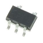
| 产品图片 |
|
| rohs | 符合RoHS无铅 / 符合限制有害物质指令(RoHS)规范要求 |
| 产品系列 | 放大器 IC,运算放大器 - 运放,ON Semiconductor TLV271SN1T1G- |
| 数据手册 | |
| 产品型号 | TLV271SN1T1G |
| 产品种类 | 运算放大器 - 运放 |
| 供应商器件封装 | 5-TSOP |
| 共模抑制比—最小值 | 69 dB |
| 关闭 | No Shutdown |
| 其它名称 | TLV271SN1T1GOSCT |
| 包装 | 剪切带 (CT) |
| 压摆率 | 2.6 V/µs |
| 商标 | ON Semiconductor |
| 增益带宽生成 | 3.2 MHz |
| 增益带宽积 | 3MHz |
| 安装类型 | 表面贴装 |
| 安装风格 | SMD/SMT |
| 封装 | Reel |
| 封装/外壳 | 6-TSOP(0.059",1.50mm 宽)5 引线 |
| 封装/箱体 | TSOP-5 |
| 工作温度 | -40°C ~ 105°C |
| 工作电源电压 | 2.7 V to 16 V |
| 工厂包装数量 | 3000 |
| 放大器类型 | 通用 |
| 最大工作温度 | + 105 C |
| 最小工作温度 | - 40 C |
| 标准包装 | 1 |
| 电压-电源,单/双 (±) | 2.7 V ~ 16 V, ±1.35 V ~ 8 V |
| 电压-输入失调 | 500µV |
| 电流-电源 | 490µA |
| 电流-输入偏置 | 1pA |
| 电流-输出/通道 | 13mA |
| 电源电流 | 550 uA |
| 电路数 | 1 |
| 系列 | TLV271 |
| 转换速度 | 2.6 V/us |
| 输入偏压电流—最大 | 150 pA |
| 输入补偿电压 | 5 mV |
| 输出电流 | 13 mA |
| 输出类型 | 满摆幅 |
| 通道数量 | 1 Channel |


- 商务部:美国ITC正式对集成电路等产品启动337调查
- 曝三星4nm工艺存在良率问题 高通将骁龙8 Gen1或转产台积电
- 太阳诱电将投资9.5亿元在常州建新厂生产MLCC 预计2023年完工
- 英特尔发布欧洲新工厂建设计划 深化IDM 2.0 战略
- 台积电先进制程称霸业界 有大客户加持明年业绩稳了
- 达到5530亿美元!SIA预计今年全球半导体销售额将创下新高
- 英特尔拟将自动驾驶子公司Mobileye上市 估值或超500亿美元
- 三星加码芯片和SET,合并消费电子和移动部门,撤换高东真等 CEO
- 三星电子宣布重大人事变动 还合并消费电子和移动部门
- 海关总署:前11个月进口集成电路产品价值2.52万亿元 增长14.8%


PDF Datasheet 数据手册内容提取
TLV271 Single-Channel, Rail-to-Rail Output, 3 MHz BW Operational Amplifier The TLV271 operational amplifier provides rail−to−rail output operation. The output can swing within 320 mV to the positive rail and http://onsemi.com 50 mV to the negative rail. This rail−to−rail operation enables the user to make optimal use of the entire supply voltage range while taking MARKING advantage of 3 MHz bandwidth. The TLV271 can operate on supply DIAGRAM voltage as low as 2.7 V over the temperature range of −40°C to 105°C. The high bandwidth provides a slew rate of 2.4 V/(cid:2)s while only TSOP−5 5 consuming 550 (cid:2)A of quiescent current. Likewise the TLV271 can run 5 (SOT23−5) XXXAYW(cid:2) SN SUFFIX (cid:2) on a supply voltage as high as 16 V making it ideal for a broad range of 1 CASE 483 battery−operated applications. Since this is a CMOS device it has high 1 input impedance and low bias currents making it ideal for interfacing XXX = ADG (TLV271SN1T1G) to a wide variety of signal sensors. In addition it comes in a small = ADH (TLV271SN2T1G) TSOP−5 package with two pinout styles allowing for use in A = Assembly Location high−density PCB’s. Y = Year W = Work Week Features (cid:2) = Pb−Free Package • (Note: Microdot may be in either location) Rail−To−Rail Output • Wide Bandwidth: 3 MHz • High Slew Rate: 2.4 V/(cid:2)s PIN CONNECTIONS • Wide Power−Supply Range: 2.7 V to 16 V • Low Supply Current: 550 (cid:2)A OUT 1 5 VEE • Low Input Bias Current: 45 pA VDD 2 + − • Wide Temperature Range: −40°C to 105°C IN+ 3 4 IN− • Small Package: 5 Pin TSOP−5 (same as SOT23−5) • Style 1 Pinout (SN1T1) These Devices are Pb−Free, Halogen Free/BFR Free and are RoHS (Top View) Compliant A•pplications OUT 1 5 VDD Notebook Computers • Portable Instruments VEE 2 + − IN+ 3 4 IN− Style 2 Pinout (SN2T1) (Top View) ORDERING INFORMATION Device Package Shipping† TLV271SN1T1G TSOP−5 3000 / (Style 1 Pinout) (Pb−Free) Tape & Reel TLV271SN2T1G TSOP−5 3000 / (Style 2 Pinout) (Pb−Free) Tape & Reel †For information on tape and reel specifications, including part orientation and tape sizes, please refer to our Tape and Reel Packaging Specifications Brochure, BRD8011/D. © Semiconductor Components Industries, LLC, 2013 1 Publication Order Number: September, 2013 − Rev. 4 TLV271/D
TLV271 MAXIMUM RATINGS Symbol Rating Value Unit VDD Supply Voltage (Note 1) 16.5 V VID Input Differential Voltage (Note 2) (cid:2)Supply Voltage V VI Input Common Mode Voltage Range (Note 1) −0.2 V to (VDD + V 0.2 V) II Maximum Input Current (cid:2)10 mA IO Output Current Range (cid:2)100 mA Continuous Total Power Dissipation (Note 1) 200 mW TJ Maximum Junction Temperature 150 °C (cid:3)JA Thermal Resistance 333 °C/W Tstg Operating Temperature Range (free−air) −40 to 105 °C Tstg Storage Temperature −65 to 150 °C Mounting Temperature (Infrared or Convection − 20 sec) 260 °C Stresses exceeding Maximum Ratings may damage the device. Maximum Ratings are stress ratings only. Functional operation above the Recommended Operating Conditions is not implied. Extended exposure to stresses above the Recommended Operating Conditions may affect device reliability. 1. Continuous short−circuit operation to ground at elevated ambient temperature can result in exceeding the maximum allowed junction temperature of 150°C. Output currents in excess of 45 mA over long term may adversely affect reliability. Shorting output to either V+ or V− will adversely affect reliability. 2. ESD data available upon request. DC ELECTRICAL CHARACTERISTICS (VDD = 2.7V, 3.3V, 5V & (cid:2)5 V (Note 3), TA = 25°C, RL (cid:3) 10 k(cid:4) unless otherwise noted) Parameter Symbol Conditions Min Typ Max Unit Input Offset Voltage VIO VIC = VDD/2, VO = VDD/2, RL = 10 k(cid:4), RS = 50 (cid:4) 0.5 5 mV TA = −40°C to +105°C 7 Offset Voltage Drift ICVOS VIC = VDD/2, VO = VDD/2, RL = 10 k(cid:4), RS = 50 (cid:4) 2 (cid:2)V/°C Common Mode CMRR 0 V (cid:4) VIC (cid:4) VDD − 1.35 V, RS = 50 (cid:4) VDD = 2.7 V 58 70 dB Rejection Ratio TA = −40°C to +105°C 55 0 V (cid:4) VIC (cid:4) VDD − 1.35 V, RS = 50 (cid:4) VDD = 5 V 65 130 TA = −40°C to +105°C 62 0 V (cid:4) VIC (cid:4) VDD − 1.35 V, RS = 50 (cid:4) VDD = (cid:2)5 V 69 140 TA = −40°C to +105°C 66 Power Supply PSRR VDD = 2.7 V to 16 V, VIC = VDD/2, No Load 70 135 dB Rejection Ratio TA = −40°C to +105°C 65 Large Signal AVD VO(pp) = VDD/2, RL = 10 k(cid:4) VDD = 2.7 V 97 106 dB Voltage Gain TA = −40°C to +105°C 76 VO(pp) = VDD/2, RL = 10 k(cid:4) VDD = 3.3 V 97 123 TA = −40°C to +105°C 76 VO(pp) = VDD/2, RL = 10 k(cid:4) VDD = 5 V 100 127 TA = −40°C to +105°C 86 VO(pp) = VDD/2, RL = 10 k(cid:4) VDD = (cid:2)5 V 100 130 TA = −40°C to +105°C 90 Input Bias Current IB VDD = 5 V, VIC = VDD/2, VO = VDD/2, TA = 25°C 45 150 pA RS = 50 (cid:4) TA = 105°C 1000 3. VDD = ±5 V is shorthand for VDD = +5 V and VEE = −5 V. http://onsemi.com 2
TLV271 DC ELECTRICAL CHARACTERISTICS (VDD = 2.7V, 3.3V, 5V & (cid:2)5 V (Note 3), TA = 25°C, RL (cid:3) 10 k(cid:4) unless otherwise noted) Parameter Symbol Conditions Min Typ Max Unit Input Offset Current IIO VDD = 5 V, VIC = VDD/2, VO = VDD/2, TA = 25°C 45 150 pA RS = 50 (cid:4) TA = 105°C 1000 Differential Input ri(d) 1000 G(cid:4) Resistance Common−mode CIC f = 21 kHz 8 pF Input Capacitance Output Swing VOH VIC = VDD/2, IOH = −1 mA VDD = 2.7 V 2.55 2.58 V (High−level) TA = −40°C to +105°C 2.48 VIC = VDD/2, IOH = −1 mA VDD = 3.3 V 3.15 3.21 TA = −40°C to +105°C 3.00 VIC = VDD/2, IOH = −1 mA VDD = 5 V 4.8 4.93 TA = −40°C to +105°C 4.75 VIC = VDD/2, IOH = −1 mA VDD = (cid:2)5 V 4.92 4.96 TA = −40°C to +105°C 4.9 VIC = VDD/2, IOH = −5 mA VDD = 2.7 V 1.9 2.1 V TA = −40°C to +105°C 1.5 VIC = VDD/2, IOH = −5 mA VDD = 3.3 V 2.5 2.89 TA = −40°C to +105°C 2.1 VIC = VDD/2, IOH = −5 mA VDD = 5 V 4.5 4.68 TA = −40°C to +105°C 4.35 VIC = VDD/2, IOH = −5 mA VDD = (cid:2)5 V 4.7 4.78 TA = −40°C to +105°C 4.65 Output Swing VOL VIC = VDD/2, IOL = −1 mA VDD = 2.7 V 0.1 0.15 V (Low−level) TA = −40°C to +105°C 0.22 VIC = VDD/2, IOL = −1 mA VDD = 3.3 V 0.03 0.15 TA = −40°C to +105°C 0.22 VIC = VDD/2, IOL = −1 mA VDD = 5 V 0.03 0.1 TA = −40°C to +105°C 0.15 VIC = VDD/2, IOL = −1 mA VDD = (cid:2)5 V 0.05 0.08 TA = −40°C to +105°C 0.1 VIC = VDD/2, IOL = −5 mA VDD = 2.7 V 0.5 0.7 V TA = −40°C to +105°C 1.1 VIC = VDD/2, IOL = −5 mA VDD = 3.3 V 0.13 0.7 TA = −40°C to +105°C 1.1 VIC = VDD/2, IOL = −5 mA VDD = 5 V 0.13 0.4 TA = −40°C to +105°C 0.5 VIC = VDD/2, IOL = −5 mA VDD = (cid:2)5 V 0.16 0.3 TA = −40°C to +105°C 0.35 3. VDD = ±5 V is shorthand for VDD = +5 V and VEE = −5 V. http://onsemi.com 3
TLV271 DC ELECTRICAL CHARACTERISTICS (VDD = 2.7V, 3.3V, 5V & (cid:2)5 V (Note 3), TA = 25°C, RL (cid:3) 10 k(cid:4) unless otherwise noted) Parameter Symbol Conditions Min Typ Max Unit Output Current IO VO = 0.5 V from rail, VDD = 2.7 V Positive rail 4.0 mA Negative rail 5.0 VO = 0.5 V from rail, VDD = 5 V Positive rail 7.0 Negative rail 8.0 VO = 0.5 V from rail, VDD = 10 V Positive rail 13 Negative rail 12 Power Supply IDD VO = VDD/2 VDD = 2.7 V 380 560 (cid:2)A Quiescent Current VDD = 3.3 V 385 620 VDD = 5 V 390 660 VDD = 10 V 400 800 TA = −40°C to +105°C 1000 3. VDD = ±5 V is shorthand for VDD = +5 V and VEE = −5 V. AC ELECTRICAL CHARACTERISTICS (VDD = 2.7 V, 5 V, & (cid:2)5 V (Note 4), TA = 25°C, and RL (cid:3) 10 k(cid:4) unless otherwise noted) Parameter Symbol Conditions Min Typ Max Unit Unity Gain UGBW RL = 2 k(cid:4), CL = 10 pF VDD = 2.7 V 3.2 MHz Bandwidth VDD = 5 V to 3.5 10 V Slew Rate at Unity SR VO(pp) = VDD/2, RL = 10 k(cid:4), CL = 50 pF VDD = 2.7 V 1.35 2.1 V/(cid:2)S Gain TA = −40°C to +105°C 1 VO(pp) = VDD/2, RL = 10 k(cid:4), CL = 50 pF VDD = 5 V 1.45 2.3 TA = −40°C to +105°C 1.2 VO(pp) = VDD/2, RL = 10 k(cid:4), CL = 50 pF VDD = (cid:2)5 V 1.8 2.6 TA = −40°C to +105°C 1.3 Phase Margin (cid:3)m RL = 2 k(cid:4), CL = 10 pF 45 ° Gain Margin RL = 2 k(cid:4), CL = 10 pF 14 dB Settling Time to tS V−step(pp) = 1 V, AV = −1, RL = 2 k(cid:4), VDD = 2.7 V 2.9 (cid:2)S 0.1% CL = 10 pF V−step(pp) = 1 V, AV = −1, RL = 2 k(cid:4), VDD = 5 V, 2.0 CL = 47 pF (cid:2)5 V Total Harmonic THD+N VDD = 2.7 V, VO(pp) = VDD/2, RL = 2 k(cid:4), AV = 1 0.004 % Distortion plus f = 10 kHz Noise AV = 10 0.04 AV = 100 0.3 VDD = 5 V, (cid:2) 5 V, VO(pp) = VDD/2, RL = AV = 1 0.004 2 k(cid:4), f = 10 kHz AV = 10 0.04 AV = 100 0.03 Input−Referred en f = 1 kHz 30 nV/√Hz Voltage Noise f = 10 kHz 20 Input−Referred in f = 1 kHz 0.6 fA/√Hz Current Noise 4. VDD = ±5 V is shorthand for VDD = +5 V and VEE = −5 V. http://onsemi.com 4
TLV271 0 A) 250 −10 RL2 =5 °2C k(cid:4) NT (p 200 E −20 R R U 150 −30 C dB) −40 SET 100 R ( FF R −50 O 50 Input Bias M 2.5 V D C −60 N −70 2.7 V 5 V AS A 0 Input Offset BI −50 −80 T 10 V U P −90 N−100 10 100 1k 10k 100k 1M I −40 −25 −10 5 20 35 50 65 80 95 110 125 FREQUENCY (Hz) FREE AIR TEMPERATURE (°C) Figure 1. CMRR vs. Frequency Figure 2. Input Bias and Offset Current vs. Temperature 2.5 2.5 GE (V) 2 VDD = 2.5 V 105°C 25°C GE (V) 2 VDD = 2.5 V A A OLT OLT −40°C T V 1.5 T V 1.5 PU −40°C PU 105°C 25°C T T OU 1 OU 1 L L E E V V LE 0.5 LE 0.5 W H G O L 0 HI 0 0 10 20 30 40 50 60 70 80 0 10 20 30 40 50 60 70 80 LOW LEVEL OUTPUT CURRENT (mA) LOW LEVEL OUTPUT CURRENT (mA) Figure 3. 2.5 V V vs. I Figure 4. 2.5 V V vs. I OL out OH out 3.3 3.3 E (V) 3 VDD = 3.3 V 25°C E (V) 3 VDD = 3.3 V G 2.7 G 2.7 TA 2.4 105°C TA 2.4 L L VO 2.1 VO 2.1 105°C T T U 1.8 U 1.8 UTP 1.5 −40°C UTP 1.5 25°C L O 1.2 L O 1.2 E E V 0.9 V 0.9 E E W L 0.6 H L 0.6 −40°C LO 0.3 HIG 0.3 0 0 0 10 20 30 40 50 60 70 80 90 0 10 20 30 40 50 60 70 80 90 LOW LEVEL OUTPUT CURRENT (mA) HIGH LEVEL OUTPUT CURRENT (mA) Figure 5. 3.3 V V vs. I Figure 6. 3.3 V V vs. I OL out OH out http://onsemi.com 5
TLV271 5 5 V) VDD = 5.0 V V) VDD = 5.0 V GE ( 4 105°C GE ( 4 A A T T L L O O T V 3 −40°C T V 3 U U P P OUT 2 25°C OUT 2 −40°C EL EL 25°C 105°C V V E 1 E 1 L L W H O G L HI 0 0 0 10 20 30 40 50 60 70 80 0 10 20 30 40 50 60 70 80 LOW LEVEL OUTPUT CURRENT (mA) HIGH LEVEL OUTPUT CURRENT (mA) Figure 7. V vs. I Figure 8. V vs. I OL out OH out 10 10 V) 9 VDD = 10 V V) 9 VDD = 10 V E ( E ( G 8 G 8 A A OLT 7 OLT 7 T V 6 105°C T V 6 25°C PU 5 PU 5 T T VEL OU 43 25°C VEL OU 43 −40°C 105°C OW LE 21 −40°C GH LE 21 L 0 HI 0 0 10 20 30 40 50 60 70 80 0 10 20 30 40 50 60 70 80 90 100 110120 LOW LEVEL OUTPUT CURRENT (mA) HIGH LEVEL OUTPUT CURRENT (mA) Figure 9. 10 V V vs. I Figure 10. 10 V V vs. I OL out OH out 12 600 11 AV = 10 105°C 10 VDD = 10 V RL = 2k A)500 V) 98 CTTLHA D== 12=05 5 °p%CF T / Ch (m400 25°C P−P ( 76 REN300 −40°C ut 5 VDD = 5 V UR Vo 4 Y C200 L 3 VDD = 2.7 V PP U100 2 VDD = 2.5 V S 1 0 0 0.01 0.1 1 10 100 1k 10k 0 2 4 6 8 10 12 14 16 18 FREQUENCY (kHz) SUPPLY VOLTAGE (V) Figure 11. Peak−to−Peak Output vs. Supply vs. Figure 12. Supply Current vs. Supply Voltage Frequency http://onsemi.com 6
TLV271 0 −10 RL = 2 k(cid:4), Input = 200 mVpp, −20 AV = 1, −30 VDD = 2.5 V to 10 V, −40 TA = 25°C B) d −50 R ( R −60 S P −70 −80 −90 −100 −110 100 1k 10k 100k FREQUENCY (Hz) Figure 13. PSRR vs. Frequency 140 180 120 Phase 2.7 V dB) 100 Phase 135 C) GAIN ( 80 G10a iVn 5 V °GIN ( P 60 90 AR O Phase M N LO 40 Gain 10 V ASE E 20 5 V H P 45 P O Gain 0 2.7 V −20 0 1 10 100 1k 10k 100k 1M 10M FREQUENCY (Hz) Figure 14. Open Loop Gain and Phase vs. Frequency 4.5 4 SR+ @ 25°C SR+ @ 105°C SR− @ 105°C 4 10 V 5 V Hz) s) 3 NCY (M 3.5 (cid:2)ATE (V/ 2 E R QU 3 W SR− @ 25°C RE 2.7 V 2.5 V LE SR− @ −40°C F S 1 2.5 SR+ @ −40°C RL = 2k CL = 10 pF 2 0 −40 −20 0 20 40 60 80 100 0 0.5 1 1.5 2 2.5 3 3.5 TEMPERATURE (°C) SUPPLY VOLTAGE (V) Figure 15. Gain Bandwidth Product vs. Figure 16. Slew Rate vs. Supply Voltage Temperature http://onsemi.com 7
TLV271 4 10k SR− 5 V SR+ 5 V VS = ±2.5 V SR− 10 V SR+ 10 V Vin = GND, z) Av = 22 RTI H 1k (cid:2)E (V/s) 3 √SE (nV AT OI 100 R N W SR+ 2.7 V SR− 2.7 V E G SLE 2 LTA 10 O V 1 1 −60 −40 −20 0 20 40 60 80 100 120 1 10 100 1k 10k 100k FREE AIR TEMPERATURE (°C) FREQUENCY (Hz) Figure 17. Slew Rate vs. Temperature Figure 18. Voltage Noise vs. Frequency VS = ±1.25 V VS = +2.5 V Av = −1 Av = +1 RL = 2 k(cid:4) RL = 2 k(cid:4) v v di di V/ V/ m m 0 0 5 5 2 2 500 ns/div 500 ns/div Figure 19. 2.5 V Inverting Large Signal Pulse Figure 20. 2.5 V Non−Inverting Large Signal Response Pulse Response VS = ±1.25 V VS = +2.5 V Av = −1 Av = +1 RL = 2 k(cid:4) RL = 2 k(cid:4) v v di di V/ V/ m m 5 5 2 2 500 ns/div 500 ns/div Figure 21. 2.5 V Inverting Small Signal Pulse Figure 22. 2.5 V Non−Inverting Small Signal Response Pulse Response http://onsemi.com 8
TLV271 VS = ±1.5 V VS = +3 V Av = +1 Av = −1 RL = 2 k(cid:4) RL = 2 k(cid:4) v v di di V/ V/ m m 0 0 5 5 2 2 500 ns/div 500 ns/div Figure 23. 3 V Inverting Large Signal Pulse Figure 24. 3 V Non−Inverting Large Signal Response Pulse Response VS = ±1.5 V VS = +3 V Av = +1 Av = −1 RL = 2 k(cid:4) RL = 2 k(cid:4) v v di di V/ V/ m m 5 5 2 2 500 ns/div 500 ns/div Figure 25. 3 V Inverting Small Signal Pulse Figure 26. 3 V Non−Inverting Small Signal Response Pulse Response VS = ±3 V VS = +6 V Av = −1 Av = +1 RL = 2 k(cid:4) RL = 2 k(cid:4) v v di di V/ V/ m m 0 0 0 0 5 5 500 ns/div 500 ns/div Figure 27. 6 V Inverting Large Signal Pulse Figure 28. 6 V Non−Inverting Large Signal Response Pulse Response http://onsemi.com 9
TLV271 VS = +6 V VS = +6 V Av = −1 Av = +1 RL = 2 k(cid:4) RL = 2 k(cid:4) v v di di V/ V/ m m 5 5 2 2 500 ns/div 500 ns/div Figure 29. 6 V Inverting Small Signal Pulse Figure 30. 6 V Non−Inverting Small Signal Response Pulse Response http://onsemi.com 10
TLV271 APPLICATIONS 50 k R1 5.0 k VDD R2 − VDD Vref 10 k − VDD TLV271 VO MC1403 2.5 V +TLV271 VO Vref(cid:5)12VDD + fO(cid:5)2(cid:5)1RC For:fo = 1.0 kHz VO(cid:5)2.5V(1(cid:6)RR12) R C R C RC == 01.60 1k(cid:4) (cid:2)F Figure 31. Voltage Reference Figure 32. Wien Bridge Oscillator VDD C R3 R1 C Vin − CO R2 TLV271 VO Hysteresis + CO = 10 C R2 VOH Vref R1 + VO Vref TLV271 Vin − VO Given: fo = center frequency VOL A(fo) = gain at center frequency VinL VinH V L(cid:5) R1 (V (cid:7)VVref (cid:6)V CThhoeons:e vaRlu3e(cid:5) fo, CQ in R1(cid:6)R2 OL ref) ref (cid:5)f C O VinH(cid:5)R1R(cid:6)1R2 (VOH(cid:7)Vref)(cid:6)Vref R1(cid:5)2AR(3f ) R1 O H(cid:5) (V (cid:7)V ) R1R3 R1(cid:6)R2 OH OL R2(cid:5) 4Q2R1(cid:7)R3 Figure 33. Comparator with Hysteresis For less than 10% error from operational amplifier, ((QO fO)/BW) < 0.1 where fo and BW are expressed in Hz. If source impedance varies, filter may be preceded with voltage follower buffer to stabilize filter parameters. Figure 34. Multiple Feedback Bandpass Filter http://onsemi.com 11
TLV271 PACKAGE DIMENSIONS TSOP−5 CASE 483−02 ISSUE K NOTES: 1. DIMENSIONING AND TOLERANCING PER ASME NOTE 5 D5X Y14.5M, 1994. 2. CONTROLLING DIMENSION: MILLIMETERS. 0.20 C A B 3. MAXIMUM LEAD THICKNESS INCLUDES LEAD FINISH 2X 0.10 T THICKNESS. MINIMUM LEAD THICKNESS IS THE MINIMUM THICKNESS OF BASE MATERIAL. M 4. DIMENSIONS A AND B DO NOT INCLUDE MOLD 2X 0.20 T B 5 4 S FFLLAASSHH,, PPRROOTTRRUUSSIIOONNSS,, OORR GGAATTEE BBUURRRRSS. SMHOALLDL NOT 1 2 3 EXCEED 0.15 PER SIDE. DIMENSION A. K 5. OPTIONAL CONSTRUCTION: AN ADDITIONAL B G DETAIL Z TTRRIIMMMMEEDD LLEEAADD INSO ATL TLOO WEXETDE INND T HMIOS RLEO CTHATAINO N0..2 A A FROM BODY. MILLIMETERS TOP VIEW DIM MIN MAX A 3.00 BSC B 1.50 BSC DETAIL Z C 0.90 1.10 J D 0.25 0.50 C G 0.95 BSC H 0.01 0.10 0.05 J 0.10 0.26 H C SPELAATNIENG END VIEW MK 0.02 0(cid:3) 010.6 (cid:3) 0 SIDE VIEW S 2.50 3.00 SOLDERING FOOTPRINT* 1.9 0.074 0.95 0.037 2.4 0.094 1.0 0.039 0.7 (cid:8) (cid:9) 0.028 SCALE 10:1 mm inches *For additional information on our Pb−Free strategy and soldering details, please download the ON Semiconductor Soldering and Mounting Techniques Reference Manual, SOLDERRM/D. ON Semiconductor and are registered trademarks of Semiconductor Components Industries, LLC (SCILLC). SCILLC reserves the right to make changes without further notice to any products herein. SCILLC makes no warranty, representation or guarantee regarding the suitability of its products for any particular purpose, nor does SCILLC assume any liability arising out of the application or use of any product or circuit, and specifically disclaims any and all liability, including without limitation special, consequential or incidental damages. “Typical” parameters which may be provided in SCILLC data sheets and/or specifications can and do vary in different applications and actual performance may vary over time. All operating parameters, including “Typicals” must be validated for each customer application by customer’s technical experts. SCILLC does not convey any license under its patent rights nor the rights of others. SCILLC products are not designed, intended, or authorized for use as components in systems intended for surgical implant into the body, or other applications intended to support or sustain life, or for any other application in which the failure of the SCILLC product could create a situation where personal injury or death may occur. Should Buyer purchase or use SCILLC products for any such unintended or unauthorized application, Buyer shall indemnify and hold SCILLC and its officers, employees, subsidiaries, affiliates, and distributors harmless against all claims, costs, damages, and expenses, and reasonable attorney fees arising out of, directly or indirectly, any claim of personal injury or death associated with such unintended or unauthorized use, even if such claim alleges that SCILLC was negligent regarding the design or manufacture of the part. SCILLC is an Equal Opportunity/Affirmative Action Employer. This literature is subject to all applicable copyright laws and is not for resale in any manner. PUBLICATION ORDERING INFORMATION LITERATURE FULFILLMENT: N. American Technical Support: 800−282−9855 Toll Free ON Semiconductor Website: www.onsemi.com Literature Distribution Center for ON Semiconductor USA/Canada P.O. Box 5163, Denver, Colorado 80217 USA Europe, Middle East and Africa Technical Support: Order Literature: http://www.onsemi.com/orderlit Phone: 303−675−2175 or 800−344−3860 Toll Free USA/Canada Phone: 421 33 790 2910 Fax: 303−675−2176 or 800−344−3867 Toll Free USA/Canada Japan Customer Focus Center For additional information, please contact your local Email: orderlit@onsemi.com Phone: 81−3−5817−1050 Sales Representative http://onsemi.com TLV271/D 12
Mouser Electronics Authorized Distributor Click to View Pricing, Inventory, Delivery & Lifecycle Information: O N Semiconductor: TLV271SN1T1G TLV271SN2T1G