ICGOO在线商城 > 集成电路(IC) > 线性 - 模拟乘法器,除法器 > AD532SH
 Datasheet下载
- 型号: AD532SH
- 制造商: Analog
- 库位|库存: xxxx|xxxx
- 要求:
| 数量阶梯 | 香港交货 | 国内含税 |
| +xxxx | $xxxx | ¥xxxx |
查看当月历史价格
查看今年历史价格
AD532SH产品简介:
ICGOO电子元器件商城为您提供AD532SH由Analog设计生产,在icgoo商城现货销售,并且可以通过原厂、代理商等渠道进行代购。 AD532SH价格参考¥询价-¥询价。AnalogAD532SH封装/规格:线性 - 模拟乘法器,除法器, Analog Multiplier/Divider 4-Quadrant TO-100-10。您可以下载AD532SH参考资料、Datasheet数据手册功能说明书,资料中有AD532SH 详细功能的应用电路图电压和使用方法及教程。
AD532SH 是 Analog Devices Inc. 生产的一款模拟乘法器/除法器集成电路,属于高性能模拟信号处理器件。该芯片可实现两个模拟信号的乘法或除法运算,广泛应用于需要实时模拟信号处理的场合。

其主要应用场景包括:

1. 自动增益控制(AGC)电路:通过将输出信号与参考信号相乘,调节增益以维持输出电平稳定。
2. 调制与解调电路:在通信系统中用于实现幅度调制(AM)、频率调制(FM)及其解调功能。
3. 功率测量与控制系统:通过乘法运算计算电压和电流的乘积,从而实现对交流或直流功率的实时监测与控制。
4. 信号调理与处理:用于传感器信号的线性化、温度补偿等处理,提升测量精度。
5. 函数发生器与波形合成:用于生成复杂波形或实现非线性函数变换。
6. 工业过程控制系统:在PID控制、比例控制等系统中实现高精度模拟运算。

AD532SH 具有宽电源电压范围、高精度和良好的温度稳定性,适用于要求较高的工业、通信和测试测量设备中。
| 参数 | 数值 |
| 产品目录 | 集成电路 (IC)半导体 |
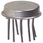
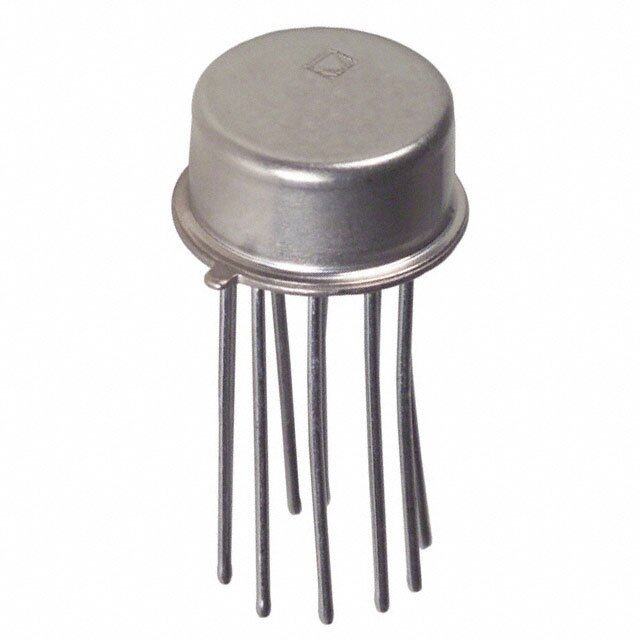
| 描述 | IC MULTIPLIER 10V TO-100-10增效器/分频器 MLTIPLIER/DIVIDER IC |
| 产品分类 | |
| 品牌 | Analog Devices |
| 产品手册 | |
| 产品图片 |
|
| rohs | 否不符合限制有害物质指令(RoHS)规范要求 |
| 产品系列 | 逻辑集成电路,增效器/分频器,Analog Devices AD532SH- |
| 数据手册 | |
| 产品型号 | AD532SH |
| 产品 | Multiplier |
| 产品种类 | 增效器/分频器 |
| 位/级数 | 四象限 |
| 供应商器件封装 | TO-100-10 |
| 功能 | 模拟乘法器/除法器 |
| 包装 | 散装 |
| 商标 | Analog Devices |
| 安装风格 | Through Hole |
| 封装 | Bulk |
| 封装/外壳 | TO-100-10 金属罐 |
| 封装/箱体 | TO-100-10 |
| 工作电源电压 | 22 V |
| 工厂包装数量 | 100 |
| 最大工作温度 | + 125 C |
| 最小工作温度 | - 55 C |
| 标准包装 | 1 |
| 电源电流 | 6 mA |
| 电路数量 | 1 |
| 系列 | AD532 |
| 输入电压 | 10 V |
| 输出电压 | 10 V |
| 逻辑系列 | AD532 |


- 商务部:美国ITC正式对集成电路等产品启动337调查
- 曝三星4nm工艺存在良率问题 高通将骁龙8 Gen1或转产台积电
- 太阳诱电将投资9.5亿元在常州建新厂生产MLCC 预计2023年完工
- 英特尔发布欧洲新工厂建设计划 深化IDM 2.0 战略
- 台积电先进制程称霸业界 有大客户加持明年业绩稳了
- 达到5530亿美元!SIA预计今年全球半导体销售额将创下新高
- 英特尔拟将自动驾驶子公司Mobileye上市 估值或超500亿美元
- 三星加码芯片和SET,合并消费电子和移动部门,撤换高东真等 CEO
- 三星电子宣布重大人事变动 还合并消费电子和移动部门
- 海关总署:前11个月进口集成电路产品价值2.52万亿元 增长14.8%


PDF Datasheet 数据手册内容提取
Internally Trimmed Integrated Circuit Multiplier Data Sheet AD532 FEATURES FUNCTIONAL BLOCK DIAGRAM Pretrimmed to ±1.0% (AD532K) VX X1 No external components required X2 Guaranteed ±1.0% maximum 4-quadrant error (AD532K) R R X Z Differential inputs for (X − X) (Y − Y)/10 V transfer function 1 2 1 2 Monolithic construction, low cost VY Y1 OUTPUT Y2 APPLICATIONS 10R VOS MAlugletbiprlaicica ctioomn,p duitvaitsiioonn , squaring, square rooting (VWOIUTTH = Z(X T1I E–D X T21)0O (V YO1U –T YP2U)T) R 00502-003 Power measurements Figure 1. Instrumentation applications GUARANTEED PERFORMANCE OVER Available in chip form TEMPERATURE GENERAL DESCRIPTION The AD532J and AD532K are specified for maximum multiplying The AD532 is the first pretrimmed, single chip, monolithic errors of ±2% and ±1% of full scale, respectively at 25°C, and multiplier/divider. It guarantees a maximum multiplying error are rated for operation from 0°C to 70°C. The AD532S has a of ±1.0% and a ±10 V output voltage without the need for any maximum multiplying error of ±1% of full scale at 25°C; it is external trimming resistors or output op amp. Because the AD532 also 100% tested to guarantee a maximum error of ±4% at the is internally trimmed, its simplicity of use provides design extended operating temperature limits of −55°C and +125°C. engineers with an attractive alternative to modular multipliers, All devices are available in either a hermetically sealed TO-100 and its monolithic construction provides significant advantages metal can or 14-lead D-14 side brazed ceramic DIP. The J, K, in size, reliability, and economy. Further, the AD532 can be a and S grade chips are also available. direct replacement for other IC multipliers that require external ADVANTAGES OF ON THE CHIP TRIMMING OF trim networks. THE MONOLITHIC AD532 FLEXIBILITY OF OPERATION 1. True ratiometric trim for improved power supply rejection. The AD532 multiplies in four quadrants with a transfer function of 2. Reduced power requirements since no networks across (X1 − X2)(Y1 − Y2)/10 V, divides in two quadrants with a 10 V Z/ supplies are required. (X1 − X2) transfer function, and square roots in one quadrant 3. More reliable because standard monolithic assembly with a transfer function of 10V Z . In addition to these basic techniques can be used rather than more complex hybrid functions, the differential X and Y inputs provide significant approaches. operating flexibility both for algebraic computation and transducer 4. High impedance X and Y inputs with negligible circuit instrumentation applications. Transfer functions, such as XY/10 V, loading. (X2 − Y2)/10 V, ±X2/10 V, and 10 V Z/(X − X), are easily attained 5. Differential X and Y inputs for noise rejection and additional 1 2 computational flexibility. and are extremely useful in many modulation and function generation applications, as well as in trigonometric calculations for airborne navigation and guidance applications, where the monolithic construction and small size of the AD532 offer considerable system advantages. In addition, the high common- mode rejection ratio (CMRR) (75 dB) of the differential inputs makes the AD532 especially well qualified for instrumentation applications, as it can provide an output signal that is the product of two transducer generated input signals. Rev. E Document Feedback Information furnished by Analog Devices is believed to be accurate and reliable. However, no responsibility is assumed by Analog Devices for its use, nor for any infringements of patents or other One Technology Way, P.O. Box 9106, Norwood, MA 02062-9106, U.S.A. rights of third parties that may result from its use. Specifications subject to change without notice. No license is granted by implication or otherwise under any patent or patent rights of Analog Devices. Tel: 781.329.4700 ©2001–2015 Analog Devices, Inc. All rights reserved. Trademarks and registered trademarks are the property of their respective owners. Technical Support www.analog.com
AD532 Data Sheet TABLE OF CONTENTS Features .............................................................................................. 1 Functional Description .....................................................................9 Applications ....................................................................................... 1 AD532 Performance Characteristics ........................................... 10 General Description ......................................................................... 1 Nonlinearity ................................................................................ 10 Flexibility of Operation .................................................................... 1 AC Feedthrough ......................................................................... 10 Functional Block Diagram .............................................................. 1 Common-Mode Rejection ........................................................ 10 Guaranteed Performance Over Temperature ............................... 1 Dynamic Characteristics ........................................................... 10 Advantages of On The Chip Trimming of The Monolithic Power Supply Considerations ................................................... 10 AD532 ................................................................................................ 1 Noise Characteristics ................................................................. 10 Revision History ............................................................................... 2 Applications ..................................................................................... 11 Specifications ..................................................................................... 3 Replacing Other IC Multipliers ................................................ 11 Thermal Resistance .......................................................................... 5 Square Root ................................................................................. 12 Chip Dimensions And Bonding Diagram ................................ 5 Difference of Squares ................................................................. 12 ESD Caution .................................................................................. 5 Additional Information ............................................................. 12 Pin Configuration and Function Descriptions ............................. 6 Outline Dimensions ....................................................................... 13 Typical Performance Characteristics ............................................. 7 Ordering Guide .......................................................................... 13 REVISION HISTORY 9/15—Rev. D to Rev. E Deleted E-20-1 Package ................................................ Throughout Changes to Guaranteed Performance Over Temperature Section ... 1 Deleted Figure 4; Renumbered Sequentially ................................. 6 Deleted Table 4; Renumbered Sequentially .................................. 7 Changes to Figure 14, Figure 15, and Figure 16 ......................... 11 Changes to Figure 17 and Figure 18 ............................................. 12 Added Additional Information Section ....................................... 12 Updated Outline Dimensions ....................................................... 13 Changes to Ordering Guide .......................................................... 14 2/11—Rev. C to Rev. D Updated Format .................................................................. Universal Added Pin Configuration and Function Descriptions Section .. 6 Added Typical Performance Characteristics Section .................. 8 Changes to Figure 11 ........................................................................ 8 Changes to Figure 12 and Figure 13 ............................................... 9 Changes to Ordering Guide .......................................................... 15 2/01—Revision 0: Initial Version Rev. E | Page 2 of 14
Data Sheet AD532 SPECIFICATIONS At 25°C, V = ±15 V, R ≥ 2 kΩ V grounded, unless otherwise noted. S OS Table 1. AD532J AD532K AD532S Model Test Conditions Min Typ Max Min Typ Max Min Typ Max Unit MULTIPLIER PERFORMANCE Transfer Function (X X )(Y Y ) (X X )(Y Y ) (X X )(Y Y ) 1 2 1 2 1 2 1 2 1 2 1 2 10V 10V 10V Total Error −10 V ≤ X, Y ≤ +10 V ±1.5 ±2.0 ±0.7 ±1.0 ±0.5 ±1.0 % TA = Minimum to Maximum ±2.5 ±1.5 ±4.0 % Total Error vs. Temperature ±0.04 ±0.03 ±0.01 ±0.04 %/°C Supply Rejection ±15 V ±10% ±0.05 ±0.05 ±0.05 %/% Nonlinearity, X X = 20 V p-p, Y = 10 V ± 0.8 ±0.5 ±0.5 % Nonlinearity, Y Y = 20 V p-p, X = 10 V ±0.3 ±0.2 ±0.2 % Feedthrough, X Y nulled, X = 20 V p-p 50 Hz 50 200 30 100 30 100 mV Feedthrough, Y (X Nulled, 30 150 25 80 25 80 mV Y = 20 V p-p 50 Hz) Feedthrough vs. 2.0 1.0 1.0 mV p-p/°C Temperature Feedthrough vs. Power ±0.25 ±0.25 ±0.25 mV/% Supply DYNAMICS Small Signal BW VOUT = 0.1 rms 1 1 1 MHz 1% Amplitude Error 75 75 75 kHz Slew Rate VOUT 20 p-p 45 45 45 V/μs Settling Time to 2%, ΔVOUT = 20 V 1 1 1 μs NOISE Wideband Noise 0.6 0.6 0.6 mV (rms) f = 5 Hz to 10 kHz f = 5 Hz to 5 MHz 3.0 3.0 3.0 mV (rms) OUTPUT Voltage Swing ±10 ±13 ±10 ±13 ±10 ±13 V Impedance f ≤ 1 kHz 1 1 1 Ω Offset Voltage ±40 ±30 ±30 mV Offset Voltage vs. 0.7 0.7 2.0 mV/°C Temperature Offset Voltage vs. Supply ±2.5 ±2.5 ±2.5 mV/% INPUT AMPLIFIERS (X, Y, and Z) Signal Voltage Range Differential or CM ±10 ±10 ±10 V operating differential CMRR 40 50 50 dB Input Bias Current X, Y Inputs 3 1.5 4 1.5 4 μA X, Y Inputs TMIN to TMAX 10 8 8 ±15 μA Z Input ±10 ±5 ±15 ±5 μA Z Input TMIN to TMAX ±30 ±25 ±25 μA Offset Current ±0.3 ±0.1 ±0.1 μA Differential Resistance 10 10 10 MΩ DIVIDER PERFORMANCE Transfer Function Xl > X2 10 V Z/(X1 − X2) 10 V Z/(X1 − X2) 10 V Z/(X1 − X2) Total Error VX = −10 V, −10 V ≤ VZ ≤ ±2 ±1 ±1 % +10 V VX = −1 V, −10 V ≤ VZ ≤ ±4 ±3 ±3 % +10 V Rev. E | Page 3 of 14
AD532 Data Sheet AD532J AD532K AD532S Model Test Conditions Min Typ Max Min Typ Max Min Typ Max Unit SQUARE PERFORMANCE (X X )2 (X X )2 (X X )2 1 2 1 2 1 2 10V 10V 10V Transfer Function Total Error ±0.8 ±0.4 ±0.4 % SQUARE ROOTER PERFORMANCE Transfer Function 10VZ 10VZ 10VZ Total Error 0 V ≤ VZ ≤ 10 V ±1.5 ±1.0 ±1.0 % POWER SUPPLY SPECIFICATIONS Supply Voltage Rated Performance ±15 ±15 ±15 V Operating ±10 ±18 ±10 ±18 ±10 ±22 V Supply Current Quiescent 4 6 4 6 4 6 mA Rev. E | Page 4 of 14
Data Sheet AD532 THERMAL RESISTANCE θJA is specified for the worst case conditions, that is, a device CHIP DIMENSIONS AND BONDING DIAGRAM soldered in a circuit board for surface-mount packages. Contact factory for the latest dimensions. Dimensions are Table 2. Thermal Resistance shown in inches and (millimeters). Package Type θ θ Unit JA JC 0.107 (2.718) H-10A 150 25 °C/W –VS OUTPUT D-14 85 22 °C/W Z X1 0.062 (1.575) +VS Y1 X2 GND VOS Y2 00502-002 Figure 2. ESD CAUTION Rev. E | Page 5 of 14
AD532 Data Sheet PIN CONFIGURATION AND FUNCTION DESCRIPTIONS Y2 Z 1 14 +VS Y1 VOS OUT 2 13 Y1 –VS 3 AD532 12 Y2 +VS AD532 GND NC 4 (NToOt Pto V SIEcaWle) 11 VOS TOP VIEW NC 5 10 GND Z (Not to Scale) X2 NC 6 9 X2 X1 7 8 NC OUT –VS X1 00502-103 DO NONTC C =O NNON ECCOTN TNOE CTTH.IS PIN. 00502-105 Figure 3. 10-Lead Header Pin Configuration (H-10) Figure 4. 14-Lead Side Brazed DIP (D-14) Table 3. 10-Lead Header Pin Function Descriptions Pin No. Mnemonic Description 1 Y Y Multiplicand Input 1 1 2 +V Positive Supply Voltage S 3 Z Dual Purpose Input 4 OUT Product Output 5 −V Negative Supply Voltage S 6 X X Multiplicand Input 1 1 7 X X Multiplicand Input 2 2 8 GND Common 9 V Output Offset Adjust OS 10 Y Y Multiplicand Input 2 2 Table 4. 14-Lead Side Brazed DIP Pin Function Descriptions Pin No. Mnemonic Description 1 Z Dual Purpose Input 2 OUT Product Output 3 −V Negative Supply Voltage S 4, 5, 6, 8 NC No Connection 7 X X Multiplicand Input 1 1 9 X X Multiplicand Input 2 2 10 GND Common 11 V Output Offset Adjust OS 12 Y Y Multiplicand Input 2 2 13 Y Y Multiplicand Input 1 1 14 +V Positive Supply Voltage S Rev. E | Page 6 of 14
Data Sheet AD532 TYPICAL PERFORMANCE CHARACTERISTICS 1 70 60 Y COMMON-MODE REJ 50 (X1 – X2) = +10V %) RTION ( 0.1 XIN YIN RR (dB) 40 X CO(YM1 M– OYN2)- M= O+D10EV REJ STO CM 30 DI 20 10 0.010 1 2 3 P4EAK5 SIGN6AL 7AMP8LITU9DE 1(V0) 11 12 13 14 00502-005 0100 1k F1R0EkQUENCY1 (0H0zk) 1M 10M 00502-008 Figure 5. Distortion vs. Peak Signal Amplitude Figure 8. CMRR vs. Frequency 100 1 20Vp-pSIGNAL RL = 2kΩ, CL = 1000pF 10 V) %) E ( ON ( TUD 0.1 RL = 2kΩ, CL = 0pF ORTI MPLI ST 1 A DI XIN YIN 0.110 100 FR1kEQUENCY1(H0kz) 100k 1M 00502-006 0.0110k 100kFREQUENCY (Hz)1M 10M 00502-009 Figure 6. Distortion vs. Frequency Figure 9. Frequency Response, Multiplying 1k 10 VZ = 0.1 × VX sin ωT GH (mV)100 Y FEEDTHROUGH E (V) HROU LITUD 1 DT MP VX = 10V EE 10 X FEEDTHROUGH A F VX = 1V VX = 5V 1100 1k F1R0EkQUENCY1 (0H0zk) 1M 10M 00502-007 0.110k 100kFREQUENCY (Hz)1M 10M 00502-010 Figure 7. Feedthrough vs. Frequency Figure 10. Frequency Response, Dividing Rev. E | Page 7 of 14
AD532 Data Sheet 14 5 V) 12 4 ± GE ( SATURASTWEIDN GOUTPUT Hz) LTA 10 µV/ 3 NAL VO MFOARX 1X% O LRI NYE IANRPIUTTY NOISE ( G 8 T 2 SI O AK SP E P 6 1 410 12 POW14ER SUPPL16Y VOLTAG18E (V) 20 22 00502-011 010 100 FREQUE1NkCY (Hz) 10k 100k 00502-012 Figure 11. Signal Swing vs. Supply Figure 12. Spot Noise vs. Frequency Rev. E | Page 8 of 14
Data Sheet AD532 FUNCTIONAL DESCRIPTION The functional block diagram for the AD532 is shown in Figure 1 The product of the two inputs is resolved in the multiplier cell and the complete schematic in Figure 13. In the multiplying and using Gilbert’s linearized transconductance technique. The cell squaring modes, Z is connected to the output to close the feedback is laser trimmed to obtain V = (X − X)(Y − Y)/10 V. The OUT 1 2 1 2 around the output op amp. In the divide mode, it is used as an built in op amp is used to obtain low output impedance and make input terminal. possible self contained operation. The residual output voltage offset can be zeroed at V in critical applications. Otherwise, the V pin The X and Y inputs are fed to high impedance differential OS OS should be grounded. amplifiers featuring low distortion and good common-mode rejection. The amplifier voltage offsets are actively laser trimmed to zero during production. X2 +VS R2 R6 R8 R16 R23 R27 Z Q1 Q2 C1 Q7 Q8 Q14Q15 Q16 Q17 Q21 R33 R34 R20 Q25 R22 Y1 R9 Q9 Q10 VOS X1 R1 Q3R3Q4 R13 R21 Q22 Q26 R31 R30 R28 COM R10 Q18 Q23 OUTPUT R29 Q5 Q6 Q11 Q12 Q24 Q27 R19 R32 R11 Q20 R14 Q19 R4 R5 Q28 R12 R15 Q13 R24 R25 R26 Y2 R18 –VS CAN 00502-004 Figure 13. Schematic Diagram Rev. E | Page 9 of 14
AD532 Data Sheet AD532 PERFORMANCE CHARACTERISTICS Multiplication accuracy is defined in terms of total error at 25°C COMMON-MODE REJECTION with the rated power supply. The value specified is in percent of The AD532 features differential X and Y inputs to enhance its full scale and includes X and Y nonlinearities, feedback and IN IN flexibility as a computational multiplier/divider. Common-mode scale factor error. To this must be added such application rejection for both inputs as a function of frequency is shown in dependent error terms as power supply rejection, common- Figure 8. It is measured with X = X = 20 V p-p, (Y − Y) = 10 V 1 2 1 2 mode rejection and temperature coefficients (although worst dc and Y = Y = 20 V p-p, (X − X) = 10 V dc. 1 2 1 2 case error over temperature is specified for the AD532S). Total DYNAMIC CHARACTERISTICS expected error is the rms sum of the individual components because they are uncorrelated. The closed-loop frequency response of the AD532 in the multiplier mode typically exhibits a 3 dB bandwidth of 1 MHz and rolls off Accuracy in the divide mode is only a little more complex. To at 6 dB/octave, thereafter. Response through all inputs is essentially achieve division, the multiplier cell must be connected in the the same as shown in Figure 9. In the divide mode, the closed- feedback of the output op amp as shown in Figure 16. In this loop frequency response is a function of the absolute value of configuration, the multiplier cell varies the closed-loop gain of the denominator voltage as shown in Figure 10. the op amp in an inverse relationship to the denominator voltage. Therefore, as the denominator is reduced, output offset, bandwidth, Stable operation is maintained with capacitive loads to 1000 pF and other multiplier cell errors are adversely affected. The divide in all modes, except the square root for which 50 pF is a safe error and drift are then εm × 10 V/(X1 − X2), where εm represents upper limit. Higher capacitive loads can be driven if a 100 Ω multiplier full-scale error and drift and (X1 − X2) is the absolute resistor is connected in series with the output for isolation. value of the denominator. POWER SUPPLY CONSIDERATIONS NONLINEARITY Although the AD532 is tested and specified with ±15 V dc Nonlinearity is easily measured in percent harmonic distortion. supplies, the device may be operated at any supply voltage from The curves of Figure 5 and Figure 6 characterize output distortion ±10 V to ±18 V for the J and K versions, and ±10 V to ±22 V as a function of input signal level and frequency respectively, for the S version. The input and output signals must be reduced with one input held at plus or minus 10 V dc. In Figure 6, the proportionately to prevent saturation; however, with supply sine wave amplitude is 20 V p-p. voltages below ±15 V, as shown in Figure 11. Because power AC FEEDTHROUGH supply sensitivity is not dependent on external null networks as in other conventionally nulled multipliers, the power supply AC feedthrough is a measure of the multiplier’s zero suppression. rejection ratios are improved from 3 to 40 times in the AD532. With one input at zero, the multiplier output should be zero NOISE CHARACTERISTICS regardless of the signal applied to the other input. Feedthrough as a function of frequency for the AD532 is shown in Figure 7. The AD532 is sampled to assure that output noise will have no It is measured for the condition VX = 0, VY = 20 V p-p and VY = 0, appreciable effect on accuracy. Typical spot noise vs. frequency VX = 20 V (p-p) over the given frequency range. It consists is shown in Figure 12. primarily of the second harmonic and is measured in millivolts peak-to-peak. Rev. E | Page 10 of 14
Data Sheet AD532 APPLICATIONS The performance and ease of use of the AD532 is achieved through Squaring the laser trimming of thin film resistors deposited directly on the monolithic chip. This trimming on the chip technique provides X1 Z a number of significant advantages in terms of cost, reliability, X2 AD532 OUT VOUT achnidp frleexsiisbtiolirtsy m ovoeurn ctoedn voern dtieopnoasli tined p oanck aa ghey btrriimd msuibnsgtr oaft eo. ff the YY12 +VS VOS –VS VOUT = V10INV2 VIN (OPTIONAL) Tanridm tmhei nagd dointi othnea lc hboipn edliinmgi nwaitreess tthhea tn aereed r feoqru air ehdy bbreitdw seuenb stthrea te +VS20kΩ–VS 00502-014 resistors and the multiplier chip. By trimming more appropriate Figure 15. Squarer Connection resistors on the AD532 chip itself, the second input terminals The squaring circuit in Figure 15 is a simple variation of the that were committed to external trimming networks have been multiplier. The differential input capability of the AD532, however, freed to allow fully differential operation at both the X and Y can obtain a positive or negative output response to the input, a inputs. Further, the requirement for an input attenuator to useful feature for control applications, as it might eliminate the adjust the gain at the Y input has been eliminated, letting the need for an additional inverter somewhere else. user take full advantage of the high input impedance properties Division of the input differential amplifiers. Therefore, the AD532 offers greater flexibility for both algebraic computation and transducer Z 10VZ instrumentation applications. X X1 Z VOUT = X X2 Provision for fine trimming the output voltage offset has been AD532 OUT VOUT Y1 included. This connection is optional, however, as the AD532 has Y2 +VS –VS been factory trimmed for total performance as described in the 1kΩ (SF) listed specifications. 47kΩ 2.2kΩ 10kΩ RExEiPstLinAg CdeINsigGn sO uTsiHngE RIC I mC uMltiUplLieTrIsP thLaItE rReqSu ire external +VS 2(0Xk0Ω) –VS 00502-015 Figure 16. Divider Connection trimming networks can be simplified using the pin for pin replaceability of the AD532 by merely grounding the X, Y, The AD532 can be configured as a two-quadrant divider by 2 2 and V terminals. The V terminal must always be grounded connecting the multiplier cell in the feedback loop of the op OS OS when unused. amp and using the Z terminal as a signal input, as shown in Figure 16. It should be noted, however, that the output error is Multiplication given approximately by 10 V ε /(X − X), where ε is the total m 1 2 m error specification for the multiply mode and bandwidth by f × X1 Z m XY21 AD532 OUT VOUT (FXu1r t−h eXr2, )t/o1 0a vVo,i wd hpeorseit fimv ei sf etehdeb baacnkd, wthied tXh ionfp tuhte i ms ruelsttirpilciteerd. to Y2 VOS (X1 – X2) (Y1 – Y2) negative values. Thus, for single-ended negative inputs (0 V to (OPTIONAL) VOUT = 10V −10 V), connect the input to X and the offset null to X2; for single- +VS 20kΩ–VS 00502-013 aenndde tdh ep oofsfistievte n iunlpl utots X (01. VFo tro o +p1ti0m Vu)m, c ponernfeocrtm thane cien,p guati nto ( SXF2 ) Figure 14. Multiplier Connection and offset (X) adjustments are recommended as shown and 0 For operation as a multiplier, the AD532 must be connected as explained in Table 5. shown in Figure 14. The inputs can be fed differentially to the X For practical reasons, the useful range in denominator input is and Y inputs or single-ended by simply grounding the unused approximately 500 mV ≤ |(X − X)| ≤ 10 V. The voltage offset 1 2 input. Connect the inputs according to the desired polarity in adjust (V ), if used, is trimmed with Z at zero and (X − X) at OS 1 2 the output. The Z terminal is tied to the output to close the full scale. feedback loop around the op amp (see Figure 1). The offset adjust V is optional and is adjusted when both inputs are zero volts OS to obtain zero out, or to null other system offsets. Rev. E | Page 11 of 14
AD532 Data Sheet Table 5. Adjustment Procedure (Divider or Square Rooter) DIFFERENCE OF SQUARES Divider Square Rooter With: Adjust for: With: Adjust for: X X1 Z X2 Adjust X Z VOUT Z VOUT AD532 OUT VOUT Scale −10 V +10 V −10 V +10 V −10 V 20kΩ 20kΩ Y1 X2 – Y2 Factor Y –Y Y2+VS VOS –VS VOUT = 10V X (Offset) −1 V +0.1 V −1 V +0.1 V −1 V 10kΩ (OPTIONAL) T0he optional scale factor and offset adjustments listed in Table 5 AD741KH +VS20kΩ–VS 00502-017 Figure 18. Differential of Squares Connection may be interactive. Repeat until satisfactory results are obtained. The differential input capability of the AD532 allows for the SQUARE ROOT algebraic solution of several interesting functions, such as the Z difference of squares, X − Y/10 V. As shown in Figure 18, the 2 2 X1 Z VOUT = 10VZ AD532 is configured in the square mode, with a simple unity X2 AD532 OUT VOUT gain inverter connected between one of the signal inputs (Y) Y1 and one of the inverting input terminals (−Y ) of the multiplier. Y2 +VS –VS IN The inverter should use precision (0.1%) resistors or be otherwise 1kΩ (SF) trimmed for unity gain for best accuracy. 47kΩ 2.2kΩ 10kΩ +VS 2(0Xk0Ω) –VS 00502-016 AFoDr aDdIdTitIiOonNalA inLfo IrNmFaOtioRnM abAouTtI tOheN a pplications for the AD532, Figure 17. Square Rooter Connection refer to the Multiplier Application Guide. The connections for square root mode are shown in Figure 17. Similar to the divide mode, the multiplier cell is connected in the feedback of the op amp by connecting the output back to both the X and Y inputs. The diode D is connected as shown to 1 prevent latch-up as Z approaches 0 V. In this case, the V IN OS adjustment is made with Z = +0.1 V dc, adjusting V to obtain IN OS −1.0 V dc in the output, V = 10V Z . For optimum OUT performance, gain (SF) and offset (X) adjustments are 0 recommended as shown and explained in Table 5. Rev. E | Page 12 of 14
Data Sheet AD532 OUTLINE DIMENSIONS 0.005 (0.13) MIN 0.080 (2.03) MAX 14 8 0.310 (7.87) 1 0.220 (5.59) 7 PIN 1 0.100 (2.54) BSC 0.320 (8.13) 0.765 (19.43) MAX 0.290 (7.37) 0.200 (5.08) 0.060 (1.52) MAX 0.015 (0.38) 0.150 (3.81) 0.200 (5.08) MIN 0.125 (3.18) 0.070 (1.78) SPELAANTIENG 00..001058 ((00..3280)) 0.023 (0.58) 0.030 (0.76) 0.014 (0.36) CONTROLLING DIMENSIONS ARE IN INCHES; MILLIMETER DIMENSIONS (IN PARENTHESES) ARE ROUNDED-OFF INCH EQUIVALENTS FOR REFERENCE ONLY AND ARE NOT APPROPRIATE FOR USE IN DESIGN. Figure 19. 14-Lead Side-Brazed Ceramic Dual In-Line Package [SBDIP] (D-14) Dimensions shown in inches and (millimeters) REFERENCE PLANE 0.185 (4.70) 0.500(12.70) 0.160 (4.06) 0.165 (4.19) MIN 0.110 (2.79) PIN 5 IS INTEGRAL CONNECHTIEOAND ETOR 6 7 0.370 (9.40) 5 0.335 (8.51) 0.021 (0.53) 0.115 8 0.016 (0.40) (2.92) 4 0.045 (1.14) 0.335 (8.51) BSC 9 0.025 (0.65) 0.305 (7.75) 3 10 0.034 (0.86) 2 1 0.025 (0.64) SIDE VIEW 0.230 (5.84) BOTTOM VIEW 0.040 (1.02) MAX BASE & SEATING PLANE BSC 36° BSC 0.050 (1.27) MAX C(RINEOFNPEATRRREOENNLDCLTIEMIHN EEOGNSN EDSLSIIYOM)ANEANSNRD SEPI AEORRRNO ESJU ENANDORDEEETC DAI N-SPO TIPFNARFCNO HIDNPEACRSRHI;AD METSEQI LM UFLOIOIVM-R0AE0 LUT6EE-SANREFT DISNI M FDOEERNSSIGIONN.S 01-19-2015-A Figure 20. 10-Pin Metal Header Package [TO-100] (H-10) Dimensions shown in inches and (millimeters) ORDERING GUIDE Model1 Temperature Range Package Description Package Option AD532JCHIPS 0°C to 70°C Chip AD532JDZ 0°C to 70°C 14-Lead Side-Brazed Ceramic Dual In-Line Package [SBDIP] D-14 AD532JHZ 0°C to 70°C 10-Pin Metal Header Package [TO-100] H-10 AD532KDZ 0°C to 70°C 14-Lead Side-Brazed Ceramic Dual In-Line Package [SBDIP] D-14 AD532KHZ 0°C to 70°C 10-Pin Metal Header Package [TO-100] H-10 AD532SCHIPS −55°C to +125°C Chip AD532SD −55°C to +125°C 14-Lead Side-Brazed Ceramic Dual In-Line Package [SBDIP] D-14 AD532SD/883B −55°C to +125°C 14-Lead Side-Brazed Ceramic Dual In-Line Package [SBDIP] D-14 AD532SH −55°C to +125°C 10-Pin Metal Header Package [TO-100] H-10 AD532SH/883B −55°C to +125°C 10-Pin Metal Header Package [TO-100] H-10 1 Z = RoHS Compliant Part. Rev. E | Page 13 of 14
AD532 Data Sheet NOTES ©2001–2015 Analog Devices, Inc. All rights reserved. Trademarks and registered trademarks are the property of their respective owners. D00502-0-9/15(E) Rev. E | Page 14 of 14