ICGOO在线商城 > 集成电路(IC) > 线性 - 模拟乘法器,除法器 > AD534JDZ
 Datasheet下载
- 型号: AD534JDZ
- 制造商: Analog
- 库位|库存: xxxx|xxxx
- 要求:
| 数量阶梯 | 香港交货 | 国内含税 |
| +xxxx | $xxxx | ¥xxxx |
查看当月历史价格
查看今年历史价格
AD534JDZ产品简介:
ICGOO电子元器件商城为您提供AD534JDZ由Analog设计生产,在icgoo商城现货销售,并且可以通过原厂、代理商等渠道进行代购。 AD534JDZ价格参考¥522.01-¥522.01。AnalogAD534JDZ封装/规格:线性 - 模拟乘法器,除法器, Analog Multiplier/Divider 4-Quadrant 14-CDIP。您可以下载AD534JDZ参考资料、Datasheet数据手册功能说明书,资料中有AD534JDZ 详细功能的应用电路图电压和使用方法及教程。
AD534JDZ 是由 Analog Devices Inc. 生产的一款线性模拟乘法器/除法器。它在各种电子系统中具有广泛的应用场景,尤其是在需要进行精确的模拟信号处理和计算的场合。以下是 AD534JDZ 的一些主要应用场景:

1. 信号调制与解调:
   - AD534JDZ 可用于实现幅度调制(AM)和解调功能。通过将输入信号与载波信号相乘,可以生成调制信号;反之,通过适当的配置,可以从调制信号中恢复原始信息。

2. 频率倍频与分频:
   - 该器件可用于生成频率是输入信号整数倍或分数倍的输出信号。例如,在锁相环(PLL)电路中,AD534JDZ 可以帮助实现频率合成和倍频功能。

3. 功率测量与控制:
   - 在电力电子和能源管理系统中,AD534JDZ 可用于实时测量电压、电流及其乘积(即功率)。通过将电压和电流信号相乘,可以直接得到瞬时功率值,从而实现高效的功率监控和控制。

4. 非线性补偿与校正:
   - 对于某些传感器或执行器,其输出特性可能存在非线性误差。AD534JDZ 可以通过乘法运算来补偿这些非线性,提高系统的精度和稳定性。

5. 音频处理与合成:
   - 在音频设备中,AD534JDZ 可用于实现音量控制、均衡器等功能。通过对不同频率成分进行加权处理,可以调整音频信号的音色和响度。

6. 科学仪器与测试设备:
   - 在精密测量仪器中,如示波器、频谱分析仪等,AD534JDZ 可用于处理复杂的模拟信号,提供高精度的测量结果。

7. 工业自动化与过程控制:
   - 在工业控制系统中,AD534JDZ 可用于实现比例积分微分(PID)控制算法中的乘法运算,从而提高控制系统的响应速度和准确性。

总之,AD534JDZ 凭借其高性能和灵活性,在众多领域中发挥着重要作用,尤其适合需要高精度模拟信号处理和数学运算的应用。
| 参数 | 数值 |
| 产品目录 | 集成电路 (IC)半导体 |
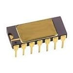
| 描述 | IC MULTIPLIER PREC TRIM 14-CDIP增效器/分频器 PREC IC Multiplier |
| 产品分类 | |
| 品牌 | Analog Devices Inc |
| 产品手册 | |
| 产品图片 |
|
| rohs | 符合RoHS无铅 / 符合限制有害物质指令(RoHS)规范要求 |
| 产品系列 | 逻辑集成电路,增效器/分频器,Analog Devices AD534JDZ- |
| 数据手册 | |
| 产品型号 | AD534JDZ |
| 产品 | Multiplier & Divider |
| 产品目录页面 | |
| 产品种类 | 增效器/分频器 |
| 位/级数 | 四象限 |
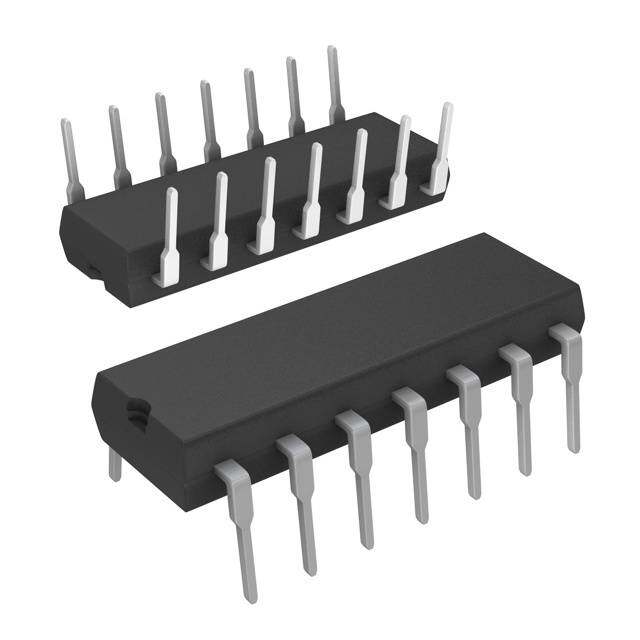
| 供应商器件封装 | 14-CDIP |
| 功能 | 模拟乘法器/除法器 |
| 包装 | 管件 |
| 商标 | Analog Devices |
| 安装风格 | Through Hole |
| 封装 | Tube |
| 封装/外壳 | 14-CDIP(0.300",7.62mm) |
| 封装/箱体 | CDIP-14 SB |
| 工作电源电压 | 15 V |
| 工厂包装数量 | 25 |
| 最大功率耗散 | 500 mW |
| 最大工作温度 | + 70 C |
| 最小工作温度 | 0 C |
| 标准包装 | 1 |
| 电源电流 | 4 mA |
| 电路数量 | 1 |
| 系列 | AD534 |
| 输入电压 | 10 V |
| 输出电压 | 11 V |
| 逻辑系列 | AD534 |


- 商务部:美国ITC正式对集成电路等产品启动337调查
- 曝三星4nm工艺存在良率问题 高通将骁龙8 Gen1或转产台积电
- 太阳诱电将投资9.5亿元在常州建新厂生产MLCC 预计2023年完工
- 英特尔发布欧洲新工厂建设计划 深化IDM 2.0 战略
- 台积电先进制程称霸业界 有大客户加持明年业绩稳了
- 达到5530亿美元!SIA预计今年全球半导体销售额将创下新高
- 英特尔拟将自动驾驶子公司Mobileye上市 估值或超500亿美元
- 三星加码芯片和SET,合并消费电子和移动部门,撤换高东真等 CEO
- 三星电子宣布重大人事变动 还合并消费电子和移动部门
- 海关总署:前11个月进口集成电路产品价值2.52万亿元 增长14.8%

PDF Datasheet 数据手册内容提取
Internally Trimmed Precision IC Multiplier Data Sheet AD534 FEATURES FUNCTIONAL BLOCK DIAGRAM Pretrimmed to ±0.25% maximum 4-quadrant error (AD534L) SF RESFTEARBELNECE +VS All inputs (X, Y, and Z) differential, high impedance for AND BIAS –VS [(X − X )(Y − Y )/10 V] + Z transfer function TRANSFER FUNCTION 1 2 1 2 2 X1 SLocawle n foaicsteo dr easdigjuns:t 9a0b lμeV t orm prso, 1v0id He zu tpo t1o0 × k1H0z0 gain X2 V-TO-1 TRANSLINEAR VOUT = A (X1 – X2S) F(Y1 – Y2) – (Z1 – Z2) MULTIPLIER Low cost, monolithic construction Y1 ELEMENT Excellent long-term stability V-TO-1 Y2 A OUT APPLICATIONS HIGH GAIN HDiigffhe rqeunatilaitly r aatniaol aongd s ipgenracle pnrtoacgees csoinmgp utations ZZ12 V-TO-1 0.75 ATTEN OAMUTPPLUIFTIER 09675-006 Algebraic and trigonometric function synthesis Figure 1. Wideband, high crest rms-to-dc conversion Accurate voltage controlled oscillators and filters Available in chip form GENERAL DESCRIPTION The AD534 is a monolithic laser trimmed four-quadrant multi- The wide spectrum of applications and the availability of several plier divider having accuracy specifications previously found grades commend this multiplier as the first choice for all new only in expensive hybrid or modular products. A maximum designs. The AD534J (±1% maximum error), AD534K (±0.5% multiplication error of ±0.25% is guaranteed for the AD534L maximum), and AD534L (±0.25% maximum) are specified for without any external trimming. Excellent supply rejection, low operation over the 0°C to +70°C temperature range. The AD534S temperature coefficients and long-term stability of the on-chip (±1% maximum) and AD534T (±0.5% maximum) are specified thin film resistors and buried Zener reference preserve accuracy over the extended temperature range, −55°C to +125°C. All even under adverse conditions of use. It is the first multiplier to grades are available in hermetically sealed TO-100 metal cans offer fully differential, high impedance operation on all inputs, and SBDIP packages. AD534K, AD534S, and AD534T chips are including the Z input, a feature that greatly increases its flexibility also available. and ease of use. The scale factor is pretrimmed to the standard value of 10.00 V; by means of an external resistor, this can be reduced to values as low as 3 V. Rev. D Document Feedback Information furnished by Analog Devices is believed to be accurate and reliable. However, no responsibility is assumed by Analog Devices for its use, nor for any infringements of patents or other One Technology Way, P.O. Box 9106, Norwood, MA 02062-9106, U.S.A. rights of third parties that may result from its use. Specifications subject to change without notice. No license is granted by implication or otherwise under any patent or patent rights of Analog Devices. Tel: 781.329.4700 ©1977–2013 Analog Devices, Inc. All rights reserved. Trademarks and registered trademarks are the property of their respective owners. Technical Support www.analog.com
AD534 Data Sheet TABLE OF CONTENTS Features .............................................................................................. 1 Functional Description .................................................................. 12 Applications ....................................................................................... 1 Provides Gain with Low Noise ..................................................... 12 Functional Block Diagram .............................................................. 1 Operation as a Multiplier .......................................................... 12 General Description ......................................................................... 1 Operation as a Squarer .............................................................. 13 Revision History ............................................................................... 2 Operation as a Divider............................................................... 13 Specifications ..................................................................................... 3 Operation as a Square Rooter ................................................... 14 Absolute Maximum Ratings ............................................................ 7 Unprecedented Flexibility ......................................................... 14 Thermal Resistance ...................................................................... 7 Applications Information .............................................................. 15 ESD Caution .................................................................................. 7 Outline Dimensions ....................................................................... 17 Pin Configurations and Function Descriptions ........................... 8 Ordering Guide .......................................................................... 18 Typical Performance Characteristics ........................................... 10 REVISION HISTORY 11/13—Rev. C to Rev. D Changed R to R in Table Summary Statements, Specifications L Section ................................................................................................ 3 Change to Pin 5, Table 5 .................................................................. 8 Change to Pin 18, Table 7 ................................................................ 9 Added Note to Figure 28 ............................................................... 17 Changes to Ordering Guide .......................................................... 18 4/11—Rev. B to Rev. C Changes to Features Section, Figure 1, and General Description Section ........................................................... 1 Added Pin Configurations and Function Descriptions Section ................................................................................................ 8 Moved Provides Gain with Low Noise Section .......................... 12 Moved Unprecedented Flexibility Section .................................. 14 Updated Outline Dimensions ....................................................... 17 Changes to Ordering Guide .......................................................... 18 Rev. D | Page 2 of 20
Data Sheet AD534 SPECIFICATIONS T = 25°C, ±V = ±15 V, R ≥ 2 kΩ, all minimum and maximum specifications are guaranteed, unless otherwise noted. A S L Table 1. AD534J AD534K AD534L Parameter Min Typ Max Min Typ Max Min Typ Max Unit MULTIPLIER PERFORMANCE Transfer Function (X X )(Y Y ) (X X )(Y Y ) (X X )(Y Y ) 1 2 1 2 Z 1 2 1 2 Z 1 2 1 2 Z 10 V 2 10 V 2 10 V 2 Total Error1 (−10 V ≤ X, Y ≤ +10 V) ±1.02 ±0.52 ±0.252 % T = T to T ±1.5 ±1.0 ±0.5 % A MIN MAX Total Error vs. Temperature ±0.022 ±0.015 ±0.008 %/°C Scale Factor Error (SF = 10.000 V Nominal)3 ±0.25 ±0.1 ±0.1 % Temperature Coefficient of Scaling Voltage ±0.02 ±0.01 ±0.005 %/°C Supply Rejection (±15 V ± 1 V) ±0.01 ±0.01 ±0.01 % Nonlinearity, X (X = 20 V p-p, ±0.4 ±0.2 ±0.32 ±0.10 ±0.122 % Y = 10 V) Nonlinearity, Y (Y = 20 V p-p, X = 10 V) ±0.2 ±0.1 ±0.12 ±0.005 ±0.12 % Feedthrough4, X (Y Nulled, ±0.3 ±0.15 ±0.32 ±0.05 ±0.122 % X = 20 V p-p 50 Hz) Feedthrough4, Y (X Nulled, ±0.01 ±0.01 ±0.12 ±0.003 ±0.12 % Y = 20 V p-p, 50 Hz) Output Offset Voltage ±5 ±302 ±2 ±152 ±2 ±102 mV Output Offset Voltage Drift 200 100 100 μV/°C DYNAMICS Small Signal BW (V = 0.1 rms) 1 1 1 MHz OUT 1% Amplitude Error (C = 1000 pF) 50 50 50 kHz LOAD Slew Rate (V 20 p-p) 20 20 20 V/μs OUT Settling Time (to 1%, D V = 20 V) 2 2 2 μs OUT NOISE Noise Spectral Density SF = 10 V 0.8 0.8 0.8 μV/√Hz SF = 3 V5 0.4 0.4 0.4 μV/√Hz Wideband Noise f = 10 Hz to 5 MHz 1 1 1 mV rms f = 10 Hz to 10 kHz 90 90 90 μV rms OUTPUT Output Voltage Swing ±112 ±112 ±112 V Output Impedance (f ≤ 1 kHz) 0.1 0.1 0.1 Ω Output Short-Circuit Current (R = 0 Ω, T = T to T ) 30 30 30 mA L A MIN MAX Amplifier Open-Loop Gain (f = 50 Hz) 70 70 70 dB INPUT AMPLIFIERS (X, Y, and Z)6 Signal Voltage Range Differential or Common Mode ±10 ±10 ±10 V Operating Differential ±12 ±12 ±12 V Offset Voltage (X, Y) ±5 ±202 ±2 ±102 ±2 ±102 mV Offset Voltage Drift (X, Y) 100 50 50 μV/°C Offset Voltage (Z) ±5 ±302 ±2 ±152 ±2 ±102 mV Offset Voltage Drift (Z) 200 100 100 μV/°C CMRR 602 80 702 90 702 90 dB Rev. D | Page 3 of 20
AD534 Data Sheet AD534J AD534K AD534L Parameter Min Typ Max Min Typ Max Min Typ Max Unit Bias Current 0.8 2.02 0.8 2.02 0.8 2.02 μA Offset Current 0.1 0.1 0.05 0.22 μA Differential Resistance 10 10 10 MΩ DIVIDER PERFORMANCE Transfer Function (X1 > X2) 10V(Z2Z1)Y 10V(Z2Z1)Y 10V(Z2Z1)Y (X X ) 1 (X X ) 1 (X X ) 1 1 2 1 2 1 2 Total Error1 X = 10 V, −10 V ≤ Z ≤ +10 V ±0.75 ±0.35 ±0.2 % X = 1 V, −1 V ≤ Z ≤ +1 V ±2.0 ±1.0 ±0.8 % 0.1 V ≤ X ≤ 10 V, −10 V ≤ Z ≤ +10 V ±2.5 ±1.0 ±0.8 % SQUARER PERFORMANCE Transfer Function (X X )2 (X X )2 (X X )2 1 2 Z 1 2 Z 1 2 Z 10V 2 10V 2 10V 2 Total Error (−10 V ≤ X ≤ +10 V) ±0.6 ±0.3 ±0.2 % SQUARE-ROOTER PERFORMANCE Transfer Function (Z ≤ Z) √(10 V(Z – Z)) + X √(10 V(Z – Z)) + X √(10 V(Z – Z)) + X 1 2 2 1 2 2 1 2 2 1 2 Total Error1 (1 V ≤ Z ≤ 10 V) ±1.0 ±0.5 ±0.25 % POWER SUPPLY SPECIFICATIONS Supply Voltage Rated Performance ±15 ±15 ±15 V Operating ±8 ±182 ±8 ±182 ±8 ±182 V Supply Current Quiescent 4 62 4 62 4 62 mA 1 Specifications given are percent of full scale, ±10 V (that is, 0.01% = 1 mV). 2 Tested on all production units at final electrical test. Results from those tests are used to calculate outgoing quality levels. 3 Can be reduced down to 3 V using external resistor between –VS and SF. 4 Irreducible component due to nonlinearity; excludes effect of offsets. 5 Using external resistor adjusted to give SF = 3 V. 6 See Figure 1 for definition of sections. Rev. D | Page 4 of 20
Data Sheet AD534 T = 25°C, ±V = ±15 V, R ≥ 2 kΩ, all minimum and maximum specifications are guaranteed, unless otherwise noted. A S L Table 2. AD534S AD534T Parameter Min Typ Max Min Typ Max Unit MULTIPLIER PERFORMANCE Transfer Function (X X )(Y Y ) (X X )(Y Y ) 1 2 1 2 Z 1 2 1 2 Z 10 V 2 10 V 2 Total Error1 (−10 V ≤ X, Y ≤ +10 V) ±1.02 ±0.52 % T = T to T ±2.02 ±1.0 % A MIN MAX Total Error vs. Temperature ±0.022 ±0.012 %/°C Scale Factor Error (SF = 10.000 V Nominal)3 ±0.25 ±0.1 % Temperature Coefficient of Scaling Voltage ±0.02 ±0.01 %/°C Supply Rejection (±15 V ± 1 V) ±0.01 ±0.01 % Nonlinearity, X (X = 20 V p-p, Y = 10 V) ±0.4 ±0.2 ±0.32 % Nonlinearity, Y (Y = 20 V p-p, X = 10 V) ±0.2 ±0.1 ±0.12 % Feedthrough4, X (Y Nulled, X = 20 V p-p, 50 Hz) ±0.3 ±0.15 ±0.32 % Feedthrough4, Y (X Nulled, Y = 20 V p-p, 50 Hz) ±0.01 ±0.01 ±0.12 % Output Offset Voltage ±5 ±302 ±2 ±152 mV Output Offset Voltage Drift 5002 3002 μV/°C DYNAMICS Small Signal BW (V = 0.1 rms) 1 1 MHz OUT 1% Amplitude Error (C = 1000 pF) 50 50 kHz LOAD Slew Rate (V 20 p-p) 20 20 V/μs OUT Settling Time (to 1%, ΔV = 20 V) 2 2 μs OUT NOISE Noise Spectral Density SF = 10 V 0.8 0.8 μV/√Hz SF = 3 V5 0.4 0.4 μV/√Hz Wideband Noise f = 10 Hz to 5 MHz 1 1 mV/rms f = 10 Hz to 10 kHz 90 90 μV/rms OUTPUT Output Voltage Swing ±112 ±112 V Output Impedance (f ≤ 1 kHz) 0.1 0.1 Ω Output Short-Circuit Current (R = 0 Ω, T = T to T ) 30 30 mA L A MIN MAX Amplifier Open-Loop Gain (f = 50 Hz) 70 70 dB INPUT AMPLIFIERS (X, Y, and Z)6 Signal Voltage Range Differential or Common Mode ±10 ±10 V Operating Differential ±12 ±12 V Offset Voltage (X, Y) ±5 ±202 ±2 ±102 mV Offset Voltage Drift (X, Y) 100 150 μV/°C Offset Voltage (Z) ±5 ±302 ±2 ±152 mV Offset Voltage Drift (Z) 5002 3002 μV/°C CMRR 602 80 702 90 dB Bias Current 0.8 2.02 0.8 2.02 μA Offset Current 0.1 0.1 μA Differential Resistance 10 10 MΩ Rev. D | Page 5 of 20
AD534 Data Sheet AD534S AD534T Parameter Min Typ Max Min Typ Max Unit DIVIDER PERFORMANCE Transfer Function (X1 > X2) 10V(Z2Z1)Y 10V(Z2Z1)Y (X X ) 1 (X X ) 1 1 2 1 2 Total Error1 X = 10 V, −10 V ≤ Z ≤ +10 V ±0.75 ±0.35 % X = 1 V, −1 V ≤ Z ≤ +1 V ±2.0 ±1.0 % 0.1 V ≤ X ≤ 10 V, −10 V ≤ Z ≤ +10 V ±2.5 ±1.0 % SQUARER PERFORMANCE Transfer Function (X X )2 (X X )2 1 2 Z 1 2 Z 10V 2 10V 2 Total Error (−10 V ≤ X ≤ +10 V) ±0.6 ±0.3 % SQUARE-ROOTER PERFORMANCE Transfer Function (Z ≤ Z) √(10 V(Z – Z)) + X √(10 V(Z – Z)) + X 1 2 2 1 2 2 1 2 Total Error1 (1 V ≤ Z ≤ 10 V) ±1.0 ±0.5 % POWER SUPPLY SPECIFICATIONS Supply Voltage Rated Performance ±15 ±15 V Operating ±8 ±222 ±8 ±222 V Supply Current Quiescent 4 62 4 62 mA 1 Specifications given are percent of full scale, ±10 V (that is, 0.01% = 1 mV). 2 Tested on all production units at final electrical test. Results from those tests are used to calculate outgoing quality levels. 3 Can be reduced down to 3 V using external resistor between –VS and SF. 4 Irreducible component due to nonlinearity: excludes effect of offsets. 5 Using external resistor adjusted to give SF = 3 V. 6 See Figure 1 for definition of sections. Rev. D | Page 6 of 20
Data Sheet AD534 ABSOLUTE MAXIMUM RATINGS X1 +VS OUT Table 3. AD534J, X2 5 AD534K, AD534S, 34 Parameter AD534L AD534T A8 Supply Voltage ±18 V ±22 V 0.076 Internal Power Dissipation 500 mW 500 mW SF (1.93) Output Short Circuit to Ground Indefinite Indefinite Z1 Input Voltages (X, X, Y, Y, 1 2 1 2 Z, Z) ±V ±V 1 2 S S Rated Operating Temperature Range 0°C to +70°C −55°C to +125°C Storage Temperature Y1 Range −65°C to +150°C −65°C to +150°C Lea6d0 Tseecm Spoeldraetruinreg R ange, 300°C 300°C Y2 0.100 (2.5–4V)S Z2 09675-004 Stresses above those listed under Absolute Maximum Ratings Figure 2. Chip Dimensions and Bonding Diagram Dimensions shown in inches and (mm) may cause permanent damage to the device. This is a stress rating only; functional operation of the device at these or any Contact factory for latest dimensions. other conditions above those indicated in the operational +VS section of this specification is not implied. Exposure to absolute 470kΩ maximum rating conditions for extended periods may affect TO APPROPRIATE 50kΩ INPUT TERMINAL device reliability. 1kΩ THERMAL RESISTANCE –VS 09675-005 θ is specified for the worst-case conditions, that is, a device Figure 3. Optional Trimming Configuration JA soldered in a circuit board for surface-mount packages. ESD CAUTION Table 4. Thermal Resistance Package Type θ θ Unit JA JC 10-Pin TO-100 (H-10) 150 25 °C/W 14-Lead SBDIP (D-14) 95 25 °C/W 20-Terminal LCC (E-20-1) 95 25 °C/W Rev. D | Page 7 of 20
AD534 Data Sheet PIN CONFIGURATIONS AND FUNCTION DESCRIPTIONS +VS X1 OUT 9 8 10 Z1 AD534 7 X2 1 TOP VIEW (Not to 6 Z2 2 Scale) SF 5 Y1 3 Y42 –VS 09675-001 Figure 4. TO-100 (H-10) Pin Configuration Table 5. H-10 Package Pin Function Descriptions Pin No. Mnemonic Description 1 X2 Inverting Differential Input of the X Multiplicand Input. 2 SF Scale Factor Input. 3 Y1 Noninverting Differential Input of the Y Multiplicand Input. 4 Y2 Inverting Differential Input of the Y Multiplicand Input. 5 −V Negative Supply Rail. Connects to header. S 6 Z2 Inverting Differential Input of the Z Reference Input. 7 Z1 Noninverting Differential Input of the Z Reference Input. 8 OUT Product Output. 9 +V Positive Supply Rail. S 10 X1 Noninverting Differential Input of the X Multiplicand Input. X1 1 14 +VS X2 2 13 NC NC 3 AD534 12 OUT SF 4 TOP VIEW 11 Z1 (Not to Scale) NC 5 10 Z2 Y1 6 9 NC Y2 7 8 –VS NCCO N=N NEOC TC OTONN TEHCIST .P DINO. NOT 09675-002 Figure 5. TO-100 (D-14) Pin Configuration Table 6. D-14 Package Pin Function Descriptions Pin No. Mnemonic Description 1 X1 Noninverting Differential Input of the X Multiplicand Input. 2 X2 Inverting Differential Input of the X Multiplicand Input. 3, 5, 9, 13 NC No Connect. Do not connect to this pin. 4 SF Scale Factor Input. 6 Y1 Noninverting Differential Input of the Y Multiplicand Input. 7 Y2 Inverting Differential Input of the Y Multiplicand Input. 8 −V Negative Supply Rail. S 10 Z2 Inverting Differential Input of the Z Reference Input. 11 Z1 Noninverting Differential Input of the Z Reference Input. 12 OUT Product Output. 14 +V Positive Supply rail. S Rev. D | Page 8 of 20
Data Sheet AD534 2 1 C VSC X X N + N 3 2 1 20 19 NC4 18OUT NC5 AD534 17NC SF6 TOP VIEW 16Z1 NC7 (Not to Scale) 15NC NC8 14Z2 9 10 11 12 13 1 2 C SC Y Y N V N NCCO N=N NEOC TC OTONN TEHC–IST .P DINO. NOT 09675-003 Figure 6. LCC (E-20-1) Pin Configuration Table 7. E-20-1 Package Pin Function Descriptions Pin No. Mnemonic Description 1, 4, 5, 7, 8, 11, 13, 15, 17, 19 NC No Connect. Do not connect to this pin. 2 X1 Noninverting Differential Input of the X Multiplicand Input. 3 X2 Inverting Differential Input of the X Multiplicand Input. 6 SF Scale Factor Input. 9 Y1 Noninverting Differential Input of the Y Multiplicand Input. 10 Y2 Inverting Differential Input of the Y Multiplicand Input. 12 −V Negative Supply Rail. S 14 Z2 Inverting Differential Input of the Z Reference Input. 16 Z1 Noninverting Differential Input of the Z Reference Input. 18 OUT Product Output. 20 +V Positive Supply Rail. S Rev. D | Page 9 of 20
AD534 Data Sheet TYPICAL PERFORMANCE CHARACTERISTICS Typical at 25°C, with ±V = ±15 V dc, unless otherwise noted. S 14 1000 L (V) OUTPUT, RL ≥ 2kΩ NA 12 VE SIG ALL INPUTS, SF = 10V p-p) 100 ATI 10 mV NEG GH ( 10 R U X-FEEDTHROUGH TIVE O 8 DTHRO POSI 6 FEE 1 Y-FEEDTHROUGH K A E P 48 10 POSITI1V2E OR NEG1A4TIVE SU1P6PLY (V)18 20 09675-020 0.110 100 1kFREQU1E0NkCY (Hz)100k 1M 10M 09675-023 Figure 7. Input/Output Signal Range vs. Supply Voltages Figure 10. AC Feedthrough vs. Frequency 800 1.5 700 Hz) T (nA)650000 SCALING VOLTAGE = 10V NSITY (µV/ 1 SCALING VOLTAGE = 10V N E E D S CURR430000 CTRAL BIA SPE0.5 SCALING VOLTAGE = 3V 200 E S OI SCALING VOLTAGE = 3V N 100 0–60 –40 –20 0 TEM20PERA40TURE6 0(°C) 80 100 120 140 09675-021 010 100 FREQUE1NkCY (Hz) 10k 100k 09675-024 Figure 8. Bias Current vs. Temperature (X, Y, or Z Input) Figure 11. Noise Spectral Density vs. Frequency 90 100 80 s) 70 V rm 90 µ CONDITIONS: 60 E ( 10Hz TO 10kHz BANDWIDTH G MRR (dB)5400 TAYLPLIC INAPL UFTOSR E VOLTA 80 C OIS 70 30 N T U 20 UTP 60 O 10 0100 1k FREQU1E0NkCY (Hz) 100k 1M 09675-022 502.5 SC5.A0LING VOLTAGE, SF7. 5(V) 10.0 09675-025 Figure 9. Common-Mode Rejection Ratio vs. Frequency Figure 12. Wideband Noise vs. Scaling Voltage Rev. D | Page 10 of 20
Data Sheet AD534 10 60 0dB = 0.1V RMS, RL = 2kΩ B) 0 40 NSE (d CL = 0pF VO( )VZ VVXZ == 1100m0mVV r mdcs O B SP–10 – d 20 PUT RE CCLF ≤= 100p0F0pF CCLF ≤≤ 1200000ppFF UTPUT VVXZ == 110V0 dmcV rms T O U O–20 0 WITH ×10 NORMAL VX = 10V dc FEEDBACK CONNECTION VZ = 1V rms ATTENUATOR –3010k 100kFREQUENCY (Hz)1M 10M 09675-026 –201k 10k FREQU1E0N0kCY (Hz) 1M 10M 09675-027 Figure 13. Frequency Response as a Multiplier Figure 14. Frequency Response vs. Divider Denominator Input Voltage Rev. D | Page 11 of 20
AD534 Data Sheet FUNCTIONAL DESCRIPTION inputs is now fully utilized. Bandwidth is unaffected by the use Figure 1 shows a functional block diagram of the AD534. Inputs of this option. are converted to differential currents by three identical voltage- to-current converters, each trimmed for zero offset. The product Supply voltages of ±15 V are generally assumed. However, of the X and Y currents is generated by a multiplier cell using satisfactory operation is possible down to ±8 V (see Figure 7). Gilbert’s translinear technique. An on-chip buried Zener Because all inputs maintain a constant peak input capability of provides a highly stable reference, which is laser trimmed to ±1.25 SF, some feedback attenuation is necessary to achieve provide an overall scale factor of 10 V. The difference between output voltage swings in excess of ±12 V when using higher XY/SF and Z is then applied to the high gain output amplifier. supply voltages. This permits various closed-loop configurations and dramati- PROVIDES GAIN WITH LOW NOISE cally reduces nonlinearities due to the input amplifiers, a The AD534 is the first general-purpose multiplier capable of dominant source of distortion in earlier designs. providing gains up to ×100, frequently eliminating the need for The effectiveness of the new scheme can be judged from the separate instrumentation amplifiers to precondition the inputs. fact that, under typical conditions as a multiplier, the nonlinear- The AD534 can be very effectively employed as a variable gain ity on the Y input, with X at full scale (±10 V), is ±0.005% of FS. differential input amplifier with high common-mode rejection. Even at its worst point, which occurs when X = ±6.4 V, nonlinear- The gain option is available in all modes and simplifies the ity is typically only ±0.05% of FS. Nonlinearity for signals applied implementation of many function-fitting algorithms such as to the X input, on the other hand, is determined almost entirely those used to generate sine and tangent. The utility of this by the multiplier element and is parabolic in form. This error is a feature is enhanced by the inherent low noise of the AD534: major factor in determining the overall accuracy of the unit and 90 μV rms (depending on the gain), a factor of 10 lower than therefore is closely related to the device grade. previous monolithic multipliers. Drift and feedthrough are also The generalized transfer function for the AD534 is given by substantially reduced over earlier designs. X X Y Y OPERATION AS A MULTIPLIER V A 1 2 1 2 Z Z OUT SF 1 2 Figure 15 shows the basic connection for multiplication. Note where: that the circuit meets all specifications without trimming. A is the open-loop gain of the output amplifier, typically X INPUT X1 +VS +15V 70 dB at dc. ±10V FS Xpe1,a Yk 1=, Z±11, .X225, SYF2,) a. nd Z2 are the input voltages (full scale = ±SF, ±12V PK XS2FAD53O4UZT1 O(XU1T –P XU21T)0, (V±Y112 –V YP2K) =+ Z2 StIhnFe mi su osthestre c dsacosawelsen, fttahoce t3 oo Vrp,. e pnr-eltoroimp mgaeidn tcoa n1 0b.0e 0r eVg abrudte dad ajsu sintafbinleit be,y ±Y±11 I20NVVP PUFKST YY12 –VZS2 –15V OINPPTUITO,N ZA, L± 1S0UVM PMKING 09675-007 and SF is 10 V. The operation performed by the AD534, can Figure 15. Basic Multiplier Connection then be described in terms of the following equation: To reduce ac feedthrough to a minimum (as in a suppressed (X − X)(Y −Y ) = 10 V (Z − Z) carrier modulator), apply an external trim voltage (±30 mV 1 2 1 2 1 2 range required) to the X or Y input (see Figure 3). Figure 10 The user can adjust SF for values between 10.00 V and 3 V by shows the typical ac feedthrough with this adjustment mode. connecting an external resistor in series with a potentiometer Note that the Y input is a factor of 10 lower than the X input between SF and −V. The approximate value of the total S and should be used in applications where null suppression is resistance for a given value of SF is given by the relationship: critical. SF R 5.4kΩ The high impedance Z terminal of the AD534 can be used to SF 10 SF 2 sum an additional signal into the output. In this mode, the Due to device tolerances, allowance should be made to vary R output amplifier behaves as a voltage follower with a 1 MHz SF by ±25% using the potentiometer. Considerable reduction in small signal bandwidth and a 20 V/μs slew rate. This terminal bias currents, noise, and drift can be achieved by decreasing SF. should always be referenced to the ground point of the driven This has the overall effect of increasing signal gain without the system, particularly if this is remote. Likewise, the differential customary increase in noise. Note that the peak input signal is inputs should be referenced to their respective ground poten- always limited to 1.25 SF (that is, ±5 V for SF = 4 V) so the tials to realize the full accuracy of the AD534. overall transfer function shows a maximum gain of 1.25. The A much lower scaling voltage can be achieved without any performance with small input signals, however, is improved by reduction of input signal range using a feedback attenuator as using a lower scale factor because the dynamic range of the shown in Figure 16. In this example, the scale is such that V = OUT Rev. D | Page 12 of 20
Data Sheet AD534 (X – X)(Y – Y), so that the circuit can exhibit a maximum If the application depends on accurate operation for inputs that 1 2 1 2 gain of 10. This connection results in a reduction of bandwidth are always less than ±3 V, the use of a reduced value of SF is recom- to about 80 kHz without the peaking capacitor C = 200 pF. In mended as described in the Functional Description section. F addition, the output offset voltage is increased by a factor of 10 Alternatively, a feedback attenuator can be used to raise the making external adjustments necessary in some applications. output level. This is put to use in the difference-of-squares Adjustment is made by connecting a 4.7 MΩ resistor between application to compensate for the factor of 2 loss involved in Z and the slider of a potentiometer connected across the generating the sum term (see Figure 20). 1 supplies to provide ±300 mV of trim range at the output. The difference of squares function is also used as the basis for a X INPUT X1 +VS +15V novel rms-to-dc converter shown in Figure 27. The averaging ±10V FS OUTPUT, ±12V PK = filter is a true integrator, and the loop seeks to zero its input. For ±12V PK X2 OUT (X1 – X2) (Y1 – Y2) this to occur, (V )2 − (V )2 = 0 V (for signals whose period is AD534 90kΩ (SCALE = 1V) IN OUT SF Z1 OPTIONAL PEAKING well below the averaging time constant). Therefore, VOUT is 10kΩ ±Y±11 I20NVVP PUFKST YY12 –VZS2 –15V CAPACITOR CF = 200pF 09675-008 tsfohigrisnc eatedlsc thnone eaiqqru ufeua lli lst h svceea rrleym, hsit i vgiash l;du aeett oemrf meVdiIniNu.e mTd h aferlm eaqbousseotn leucntiteei sra eaclncyud br yfao ctryh eo f Figure 16. Connections for Scale Factor of Unity ratio of the resistors in the inverting amplifier. The multiplier scaling voltage affects only open-loop gain. The data shown is Feedback attenuation also retains the capability for adding a typical of performance that can be achieved with an AD534K, signal to the output. Signals can be applied to the high impedance but even using an AD534J, this technique can readily provide Z terminal where they are amplified by +10 or to the common 2 better than 1% accuracy over a wide frequency range, even for ground connection where they are amplified by +1. Input signals crest factors in excess of 10. can also be applied to the lower end of the 10 kΩ resistor, giving a gain of −9. Other values of feedback ratio, up to ×100, can be OPERATION AS A DIVIDER used to combine multiplication with gain. Figure 18 shows the connection required for division. Unlike Occasionally, it may be desirable to convert the output to a earlier products, the AD534 provides differential operation on current into a load of unspecified impedance or dc level. For both numerator and denominator, allowing the ratio of two example, the function of multiplication is sometimes followed floating variables to be generated. Further flexibility results by integration; if the output is in the form of a current, a simple from access to a high impedance summing input to Y1. As with capacitor provides the integration function. Figure 17 shows all dividers based on the use of a multiplier in a feedback loop, how this can be achieved. This method can also be applied in the bandwidth is proportional to the denominator magnitude, squaring, dividing, and square rooting modes by appropriate as shown in Figure 14. ccfrhoenoqitucroeen lolcefyd t eclroomwnvi-npearatlsess.r f Tsilhhtoeisrw tanenc idhn nt thihqeeu d eAi fipfsep urliescneadtti iaionln itnsh pIenu vfto ovrlomtaltgaaetgi oe-nt o- (DENOMI±X±N11 AI20NTVVPO PUFRKST) +– XX12 O+UVTS +15V OUT1P0(UVXT 1(,Z –±2 1X–22 VZ)1 P)K+ = Y1 section. AD534 Z INPUT SF Z1 (NUMERATOR) OPTIONAL ±X±11 I20NVVP PUFKST XX12 O+UVTS CREUSRIRSETNOTR-,S RESN,S 2INkΩG MIN SU±M1I0NMVPI NPUGKT Y1 Z2 ±±1102VV FPSK Y INPUT SYF1AD534ZZ12 IOUT = (X1 – X21)0 (VY1 – Y2) ×R1S FiguYr2e 18. Ba–siVcS Divider– C15oVnnection 09675-010 ±±1120VV PFKS Y2 –VS INCT(ASEPEGAER CTAIETTXOOTRR) 09675-009 WADit5h3o4uLt aisd sduitfifoicniaenl ttr tiom mmaiinngt,a tihne a a 1c%cu errarcoyr o ofv tehre a A 1D0 5V3 4toK 1 a nVd Figure 17. Conversion of Output to Current denominator range. This range can be extended to 100:1 by OPERATION AS A SQUARER simply reducing the X offset with an externally generated trim voltage (range required is ±3.5 mV maximum) applied to the Operation as a squarer is achieved in the same fashion as the unused X input (see Figure 3). To trim, apply a ramp of +100 mV multiplier except that the X and Y inputs are used in parallel. to +V at 100 Hz to both X and Z (if X is used for offset adjust- 1 1 2 The differential inputs can be used to determine the output ment; otherwise, reverse the signal polarity) and adjust the trim polarity (positive for X = Y and X = Y, negative if either one 1 l 2 2 voltage to minimize the variation in the output of the inputs is reversed). Accuracy in the squaring mode is typically a factor of 2 better than in the multiplying mode and Because the output is near 10 V, it should be ac-coupled for the largest errors occurring with small values of output for this adjustment. The increase in noise level and reduction in input below 1 V. bandwidth preclude operation much beyond a ratio of 100 to 1. Rev. D | Page 13 of 20
AD534 Data Sheet As with the multiplier connection, overall gain can be introduced In contrast to earlier devices, which were intolerant of capacitive by inserting a simple attenuator between the output and Y loads in the square root modes, the AD534 is stable with all 2 terminal. This option and the differential ratio capability of the loads up to at least 1000 pF. For critical applications, a small AD534 are used in the percentage computer application shown adjustment to the Z input offset (see Figure 3) improves in Figure 24. This configuration generates an output propor- accuracy for inputs below 1 V. tional to the percentage deviation of one variable (A) with UNPRECEDENTED FLEXIBILITY respect to a reference variable (B), with a scale of 1% per volt. The precise calibration and differential Z input provide a degree OPERATION AS A SQUARE ROOTER of flexibility found in no other currently available multiplier. The operation of the AD534 in the square root mode is shown Standard multiplication, division, squaring, square-rooting in Figure 19. The diode prevents a latching condition, which (MDSSR) functions are easily implemented while the restriction may occur if the input momentarily changes polarity. As shown, to particular input/output polarities imposed by earlier designs the output is always positive; it can be changed to a negative has been eliminated. Signals can be summed into the output, output by reversing the diode direction and interchanging the X with or without gain and with either a positive or negative inputs. Because the signal input is differential, all combinations sense. Many new modes based on implicit function synthesis of input and output polarities can be realized, but operation is have been made possible, usually requiring only external restricted to the one quadrant associated with each combination passive components. The output can be in the form of a current, of inputs. if desired, facilitating such operations as integration. OUTPUT, ±12V PK = 10V (Z2 – Z1) + X2 RL X1 +VS +15V REVERSE THIS (MUST BE AND X INPUTS PROVIDED) FOR NEGATIVE X2 OUT OUTPUTS AD534 OPTIONAL SUMMING SF Z1 – Z INPUT INPUT ±10V FS X, ±10V PK Y1 Z2 + ±12V PK Y2 –VS –15V 09675-011 Figure 19. Square-Rooter Connection Rev. D | Page 14 of 20
Data Sheet AD534 APPLICATIONS INFORMATION The versatility of the AD534 allows the creative designer to implement a variety of circuits such as wattmeters, frequency doublers, and automatic gain controls. MODULATION X1 +VS +15V INPUT, ±EM X2 OUT OUTPUT = 1 ± 1 E 0 M V EC sin ωt AD534 A A – B X1 +VS +15V SF Z1 2 X2AD53O4UT 30kΩ OUTPUT =A21 0–V B2 CARRIEERC IsNinP UωTt Y1 Z2 SF Z1 10kΩ Y2 –VS –15V B A + B Y1 Z2 2 Y2 –VS –15V 09675-012 TSBHIIGAESN S AYFL2 PATIOMN PVOLSRI/F2 A.IC ZA ATITOTNE.N OUPAETROART CIOANN F BREO UMS AE DS ITNOG LPER OSVUIPDPEL OY VPEORSASLIBLLE; 09675-015 Figure 20. Difference of Squares Figure 23. Linear AM Modulator X1 +VS +15V CONTROL INPUT, ESC,E 0T1V kG ΩTAOIN ±5V2kΩ X2AD53O4UT 39kΩ OUTPUT, ±12V PK =E0C.1 EVS 9kΩ X1 +VS +15V –VSSIGNAL INPUT, SYF1 ZZ12 1kΩ 0.005µF 1kΩ X2AD53O4UT O(1U%T PPEURT V= O(1L0T0)V)A B– B ES, ±5V PK Y2 –VS –15V SF Z1 NOTES B INPUT, Y1 Z2 A INPUT (±) 1. GAIN IS × 10 PER VOLT OF EC, ZERO TO × 50. (+VE ONLY) 2. WIDEBAND (10HzTO 30kHz) OUTPUT NOISE IS 3mV rms, Y2 –VS –15V TYP CORRESPONDING TO A.F.S. SNR OF 70dB. 34 .. NB60OAµNIVSD ErWm RIsDE, FTTEHYR PISR. EDDC TTOO S2I0GkNHAz,L – I3NdPBU, TIN, DWEITPHE NEDC E=N ±T5 VO,F IS GAIN. 09675-013 OCATNH EBRE SOCBATLAEISN,E FDR BOYM A 1L0T%E RPIENRG V TOHLET F TEOE D0.B1A%C PKE RRA VTOIOL.T 09675-016 Figure 21. Voltage-Controlled Amplifier Figure 24. Percentage Computer X1 +VS +15V 10kΩ 18kΩ XS2FAD53O4UZT1 44..73kkΩΩ WOUHTEPRUET θ = = ( 1 π20 V )× s1iEn0θV θ XX12 O+UVTS +15V OUTPUT, ±5V/PK = 0VIN TPOU +T1, 0EVθ Y1 Z2 3kΩ SFAD534Z1 (10V)1 +y y Y WHERE y = Y2 –VS –15V INPUT, Y ±10V FS Y1 Z2 (10V) UAθ CSISICN IUGNR RCAALCODYIS AOENF TS FO.ITL EISR AWNITCHEI NR E±S0.I5S%TO ARTS A ALNLD P AODIN5T4S3L., 09675-014 Y2 –VS –15V 09675-017 Figure 22. Sine Function Generator Figure 25. Bridge Linearization Function Rev. D | Page 15 of 20
AD534 Data Sheet +15V 2kΩ ADJ 8kHz 39kΩ X1 +VS +15V 3pF to 30pF X2 OUT ADJ 2 82kΩ AD534 1kHz 7 OUTPUT 3 ±15V APPROX. SF Z1 500Ω 2.2kΩ AD211 (= R) PINS 5, 6, 8 TO +15V CEOCN10T0RmOVL TINOP 1U0TV, +– YY12 –VZS2 –15V (0=. 0C1) WPf =INI T E4S H 0C 1 V ,× A4CL 1TRUOE= S –11 kS5HHVzO PWENR VOLT CALIBRATION PROCEDURE: WITH EC = 1.0V,ADJUST POTENTIOMETERTO SET f = 1.000kHz WITH EC = 8.0V,ADJUST TRIMMER CAPACITORTO SET f = 8.000kHz. LINEARITY WILL TYPICALLY BE WITHIN ±0.1% OF FS FORANY OTHER INPUT. DUETO DELAYS IN THE COMPARATOR, THIS TECHNIQUE IS NOT SUITABLE FOR MAXIMUM FREQUENCIESABOVE 10kHz. FOR FREQUENCIESABOVE 1AU0 STkERHDIzA ATNSHGEALNAE -DOW5UA3T7V PEVU OOTLF, TA ±A 5VGVOE LP-TTKAOAG-FPERP-FEEOQALRULSEONAWCCYER RCO OSSSNH VOTEUHRLETD 0E .BR0E1 Iµ SIFN R TCEEACRPOPAMOCMSITEEODNR.D: EIFD. 09675-018 Figure 26. Differential Input Voltage-to-Frequency Converter MATCHEDTO 0.025% 20kΩ 10kΩ 10kΩ AD741K 5kΩ 10µF X1 +VS +15V INPUT NONPOLAR 10kΩ + 5V RMS FS X2 OUT ±10V PEAK 10µF SOLID Ta RMS + DC AD534 MODE 10kΩ SF Z1 O0VUTTOPU 5TV AC RMS 10kΩ Z2 AD741J Y1 10MΩ Y2 –VS +15V ZERO 20kΩ –15V ADJ CALIBRATION PROCEDURE: WITH MODE SWITCH IN ‘RMS + DC’ POSITION,APPLYAN INPUT OF +1.00V DC. ADJUST ZERO UNTIL OUTPUT READS SAMEAS INPUT. CHECK FOR INPUTS OF ±10V; OUTPUT SHOULD BE WITHIN ±0.05% (5mV). ACCURACY IS MAINTAINED FROM 60HzTO 100kHz,AND IS TYPICALLY HIGH BY 0.5%AT 1MHz FOR VIN = 4V RMS (SINE, SQUARE, OR TRIANGLULAR-WAVE). PROVIDED THAT THE PEAK INPUT IS NOT EXCEEDED, CRESTFACTORS UP TOAT LEAST 10 HAVE NOAPPRECIABLE EFFECT ONACCURACY. INPUT IMPEDANCE ISABOUT 10kΩ; FOR HIGH (10MΩ) IMPEDANCE, REMOVE MFAOSO RDA EGS UISNAWGRILTAECNHPTAEACENKDDA SIGNPEPE UCRTIMF CSICO-ATUOTPI-OLDINCNS GC T OCHNOEVMAEPDRO5T3NE6ERAN.ATSN.DAD636ARE OFFERED 09675-019 Figure 27. Wideband, High-Crest Factor, RMS-to-DC Converter Rev. D | Page 16 of 20
Data Sheet AD534 OUTLINE DIMENSIONS REFERENCE PLANE 0.500(12.70) 0.185 (4.70) MIN 0.160 (4.06) 0.110 (2.79) 0.165 (4.19) PIN 5 IS INTEGRAL CONNECHTIEOAND ETOR 6 7 0.370 (9.40) 5 0.335 (8.51) 0.021 (0.53) 0.115 8 0.016 (0.40) (2.92) 4 0.045 (1.14) 0.335 (8.51) BSC 9 0.025 (0.65) 0.305 (7.75) 3 10 0.034 (0.86) SIDE VIEW 2 1 0.025 (0.64) 0.230 (5.84) BOTTOM VIEW 0.040 (1.02) MAX BASE & SEATING PLANE BSC 36° BSC 0.050 (1.27) MAX C(RINOEFNPEATRRREOENNLDCLTIEMIHN EEOGNSN EDSLSIIYOM)ANEANSNRD SEPI AEORRRNO ESJU ENANDORDEEETC DAI N-SPO TIPFNARFCNO HDINPEACRSRHI;AD METSEQI LM UFLOIOIVM-R0AE0 LUT6EE-SANREFT DISNI M FDOEERNSSIGIONN.S 11-19-2013-A Figure 28. 10-Pin Metal Header Package [TO-100] (H-10) Pin 5 is integral connection to header Dimensions shown in inches and (millimeters) 0.005 (0.13) MIN 0.080 (2.03) MAX 14 8 0.310 (7.87) 1 0.220 (5.59) 7 PIN 1 0.100 (2.54) BSC 0.320 (8.13) 0.765 (19.43) MAX 0.290 (7.37) 0.200 (5.08) 0.060 (1.52) MAX 0.015 (0.38) 0.150 (3.81) 0.200 (5.08) MIN 0.125 (3.18) 0.070 (1.78) SPELAANTIENG 00..001058 ((00..3280)) 0.023 (0.58) 0.030 (0.76) 0.014 (0.36) CONTROLLING DIMENSIONS ARE IN INCHES; MILLIMETER DIMENSIONS (IN PARENTHESES) ARE ROUNDED-OFF INCH EQUIVALENTS FOR REFERENCE ONLY AND ARE NOT APPROPRIATE FOR USE IN DESIGN. Figure 29. 14-Lead Side-Brazed Ceramic Dual In-Line Package [SBDIP] (D-14) Dimensions shown in inches and (millimeters) 0.200 (5.08) 0.075 (1.91) REF 0.100 (2.54) REF 0.100 (2.54) REF 0.064 (1.63) 0.095 (2.41) 0.015 (0.38) 0.075 (1.90) MIN 19 3 18 20 4 0.028 (0.71) 0.358 (9.09) 0.358 1 0.342 (8.69) (9.09) 0.011 (0.28) BOTTOM 0.022 (0.56) SQ MSAQX 0.007 R(0 T.1Y8P) VIEW 0.050 (1.27) 0.075 (1.91) 14 8 BSC REF 13 9 45° TYP 0.088 (2.24) 0.055 (1.40) 0.150 (3.81) 0.054 (1.37) 0.045 (1.14) BSC C(RINOEFNPETARRREOENNLCLTEIHN EOGSN DELSIYM)AEANNRDSEI AORRNOESU NANORDEET DAIN-PO IPFNRFCO HINPECRSHI;A METEQIL UFLIOIVMRAE LUTEESNRET DISNI M FDOEERNSSIGIONN.S 022106-A Figure 30. 20-Terminal Ceramic Leadless Chip Carrier [LCC] (E-20-1) Dimensions shown in inches and (millimeters) Rev. D | Page 17 of 20
AD534 Data Sheet ORDERING GUIDE Model1 Temperature Range Package Description Package Option AD534JD 0°C to +70°C 14-Lead Side Brazed Ceramic Dual In-Line Package [SBDIP] D-14 AD534JDZ 0°C to +70°C 14-Lead Side Brazed Ceramic Dual In-Line Package [SBDIP] D-14 AD534KD 0°C to +70°C 14-Lead Side Brazed Ceramic Dual In-Line Package [SBDIP] D-14 AD534KDZ 0°C to +70°C 14-Lead Side Brazed Ceramic Dual In-Line Package [SBDIP] D-14 AD534LD 0°C to +70°C 14-Lead Side Brazed Ceramic Dual In-Line Package [SBDIP] D-14 AD534LDZ 0°C to +70°C 14-Lead Side Brazed Ceramic Dual In-Line Package [SBDIP] D-14 AD534JH 0°C to +70°C 10-Pin Metal Header Package [TO-100] H-10 AD534JHZ 0° C to +70°C 10-Pin Metal Header Package [TO-100] H-10 AD534KH 0°C to +70°C 10-Pin Metal Header Package [TO-100] H-10 AD534KHZ 0°C to +70°C 10-Pin Metal Header Package [TO-100] H-10 AD534LHZ 0°C to +70°C 10-Pin Metal Header Package [TO-100] H-10 AD534KCHIPS 0°C to +70°C Chip AD534SD −55°C to +125°C 14-Lead Side Brazed Ceramic Dual In-Line Package [SBDIP] D-14 AD534SD/883B −55°C to +125°C 14-Lead Side Brazed Ceramic Dual In-Line Package [SBDIP] D-14 AD534TD −55°C to +125°C 14-Lead Side Brazed Ceramic Dual In-Line Package [SBDIP] D-14 AD534TD/883B −55°C to +125°C 14-Lead Side Brazed Ceramic Dual In-Line Package [SBDIP] D-14 AD534SE/883B −55°C to +125°C 20-Terminal Ceramic Leadless Chip Carrier [LCC] E-20-1 AD534TE/883B −55°C to +125°C 20-Terminal Ceramic Leadless Chip Carrier [LCC] E-20-1 AD534SH −55°C to +125°C 10-Pin Metal Header Package [TO-100] H-10 AD534SH/883B −55°C to +125°C 10-Pin Metal Header Package [TO-100] H-10 AD534TH −55°C to +125°C 10-Pin Metal Header Package [TO-100] H-10 AD534TH/883B −55°C to +125°C 10-Pin Metal Header Package [TO-100] H-10 AD534SCHIPS −55°C to +125°C Chip AD534TCHIPS −55°C to +125°C Chip 1 Z = RoHS Compliant Part. Rev. D | Page 18 of 20
Data Sheet AD534 NOTES Rev. D | Page 19 of 20
AD534 Data Sheet NOTES ©1977–2013 Analog Devices, Inc. All rights reserved. Trademarks and registered trademarks are the property of their respective owners. D09675-0-11/13(D) Rev. D | Page 20 of 20
Mouser Electronics Authorized Distributor Click to View Pricing, Inventory, Delivery & Lifecycle Information: A nalog Devices Inc.: AD534LDZ AD534TH AD534KH AD534TH/883B AD534TD/883B AD534KHZ AD534KD AD534JHZ AD534JD AD534TD AD534LD AD534SD AD534SD/883B AD534SH/883B AD534SH AD534JDZ AD534TE/883B AD534KDZ AD534JH AD534SE/883B AD534LHZ