ICGOO在线商城 > 集成电路(IC) > 数据采集 - 数模转换器 > AD5324BRM
 Datasheet下载
- 型号: AD5324BRM
- 制造商: Analog
- 库位|库存: xxxx|xxxx
- 要求:
| 数量阶梯 | 香港交货 | 国内含税 |
| +xxxx | $xxxx | ¥xxxx |
查看当月历史价格
查看今年历史价格
AD5324BRM产品简介:
ICGOO电子元器件商城为您提供AD5324BRM由Analog设计生产,在icgoo商城现货销售,并且可以通过原厂、代理商等渠道进行代购。 AD5324BRM价格参考。AnalogAD5324BRM封装/规格:数据采集 - 数模转换器, 12 位 数模转换器 4 10-MSOP。您可以下载AD5324BRM参考资料、Datasheet数据手册功能说明书,资料中有AD5324BRM 详细功能的应用电路图电压和使用方法及教程。
AD5324BRM 是由 Analog Devices Inc.(亚德诺半导体)生产的一款 12 位电压输出数模转换器(DAC),属于数据采集 - 数模转换器类别。其应用场景广泛,主要应用于需要高精度、低功耗和多通道控制的系统中。以下是 AD5324BRM 的一些典型应用场景:

1. 工业自动化与过程控制
   AD5324BRM 可用于工业自动化设备中的多通道信号生成。例如,在可编程逻辑控制器(PLC)中,它能够将数字信号转换为模拟信号,用于控制阀门、电机或其他执行机构的运行状态。

2. 测试与测量设备
   在测试与测量领域,AD5324BRM 可以用来生成精确的电压信号,用于校准仪器或模拟真实世界的信号条件。例如,示波器、信号发生器等设备可以利用其高精度特性来提高测量准确性。

3. 通信系统
   在通信设备中,AD5324BRM 可以用于生成调制信号或偏置电压。它的低功耗特性和小型封装使其非常适合便携式或电池供电的通信设备。

4. 消费电子
   AD5324BRM 可用于音频设备、家用电器等需要模拟信号输出的场合。例如,音量调节、亮度控制等功能可以通过 DAC 输出实现平滑的模拟信号变化。

5. 医疗设备
   在医疗领域,AD5324BRM 可用于生成精确的刺激信号或控制信号。例如,在心电图机、超声波设备或患者监护仪中,它能够提供稳定的电压输出以驱动传感器或执行器。

6. 汽车电子
   AD5324BRM 可用于汽车电子控制系统中,如发动机管理、车身控制模块等。它可以生成精确的控制信号,用于调节燃油喷射、点火时间或其他关键参数。

7. 航空航天与国防
   在高可靠性要求的航空航天和国防应用中,AD5324BRM 可用于飞行控制系统、雷达设备或导航系统中,提供精确的模拟信号输出。

总之,AD5324BRM 凭借其 4 通道独立 DAC、12 位分辨率和 SPI 接口等特点,适用于需要多路高精度信号输出的场景,尤其在工业、通信、医疗和消费电子等领域具有广泛的适用性。
| 参数 | 数值 |
| 产品目录 | 集成电路 (IC)半导体 |
| 描述 | IC DAC 12BIT QUAD 2.5V 10-MSOP数模转换器- DAC IC 12-BIT QUAD 8uS |
| 产品分类 | |
| 品牌 | Analog Devices Inc |
| 产品手册 | |
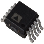
| 产品图片 |
|
| rohs | 否不符合限制有害物质指令(RoHS)规范要求 |
| 产品系列 | 数据转换器IC,数模转换器- DAC,Analog Devices AD5324BRM- |
| 数据手册 | |
| 产品型号 | AD5324BRM |
| 产品培训模块 | http://www.digikey.cn/PTM/IndividualPTM.page?site=cn&lang=zhs&ptm=19145http://www.digikey.cn/PTM/IndividualPTM.page?site=cn&lang=zhs&ptm=18614http://www.digikey.cn/PTM/IndividualPTM.page?site=cn&lang=zhs&ptm=26125http://www.digikey.cn/PTM/IndividualPTM.page?site=cn&lang=zhs&ptm=26140http://www.digikey.cn/PTM/IndividualPTM.page?site=cn&lang=zhs&ptm=26150http://www.digikey.cn/PTM/IndividualPTM.page?site=cn&lang=zhs&ptm=26147 |
| 产品种类 | 数模转换器- DAC |
| 位数 | 12 |
| 供应商器件封装 | 10-MSOP |
| 分辨率 | 12 bit |
| 包装 | 管件 |
| 商标 | Analog Devices |
| 安装类型 | 表面贴装 |
| 安装风格 | SMD/SMT |
| 封装 | Tube |
| 封装/外壳 | 10-TFSOP,10-MSOP(0.118",3.00mm 宽) |
| 封装/箱体 | MSOP-10 |
| 工作温度 | -40°C ~ 105°C |
| 工厂包装数量 | 50 |
| 建立时间 | 8µs |
| 接口类型 | SPI |
| 数据接口 | SPI, DSP |
| 最大功率耗散 | 5 mW |
| 最大工作温度 | + 105 C |
| 最小工作温度 | - 40 C |
| 标准包装 | 50 |
| 电压参考 | External |
| 电压源 | 单电源 |
| 电源电压-最大 | 5.5 V |
| 电源电压-最小 | 2.5 V |
| 积分非线性 | +/- 10 LSB |
| 稳定时间 | 8 us |
| 系列 | AD5324 |
| 结构 | Resistor String |
| 转换器数 | 4 |
| 转换器数量 | 4 |
| 输出数和类型 | 4 电压 |
| 输出类型 | Voltage |
| 采样比 | 125 kSPs |
| 采样率(每秒) | - |


- 商务部:美国ITC正式对集成电路等产品启动337调查
- 曝三星4nm工艺存在良率问题 高通将骁龙8 Gen1或转产台积电
- 太阳诱电将投资9.5亿元在常州建新厂生产MLCC 预计2023年完工
- 英特尔发布欧洲新工厂建设计划 深化IDM 2.0 战略
- 台积电先进制程称霸业界 有大客户加持明年业绩稳了
- 达到5530亿美元!SIA预计今年全球半导体销售额将创下新高
- 英特尔拟将自动驾驶子公司Mobileye上市 估值或超500亿美元
- 三星加码芯片和SET,合并消费电子和移动部门,撤换高东真等 CEO
- 三星电子宣布重大人事变动 还合并消费电子和移动部门
- 海关总署:前11个月进口集成电路产品价值2.52万亿元 增长14.8%


PDF Datasheet 数据手册内容提取
2.5 V to 5.5 V, 500 μA, Quad Voltage Output 8-/10-/12-Bit DACs in 10-Lead Packages Data Sheet AD5304/AD5314/AD5324 FEATURES GENERAL DESCRIPTION AD5304: 4 buffered 8-Bit DACs in 10-lead MSOP and The AD5304/AD5314/AD53241 are quad 8-, 10-, and 12-bit 10-lead LFCSP buffered voltage output DACs in 10-lead MSOP and 10-lead A, W Version: ±1 LSB INL, B Version: ±0.625 LSB INL LFCSP packages that operate from a single 2.5 V to 5.5 V supply, AD5314: 4 buffered 10-Bit DACs in 10-lead MSOP and consuming 500 μA at 3 V. Their on-chip output amplifiers allow 10-lead LFCSP rail-to-rail output swing to be achieved with a slew rate of 0.7 V/μs. A, W Version: ±4 LSB INL, B Version: ±2.5 LSB INL A 3-wire serial interface is used; it operates at clock rates up to AD5324: 4 buffered 12-Bit DACs in 10-lead MSOP and 30 MHz and is compatible with standard SPI, QSPI, MICROWIRE, 10-lead LFCSP and DSP interface standards. A, W Version: ±16 LSB INL, B Version: ±10 LSB INL The references for the four DACs are derived from one reference Low power operation: 500 μA @ 3 V, 600 μA @ 5 V pin. The outputs of all DACs can be updated simultaneously using 2.5 V to 5.5 V power supply the software LDAC function. The parts incorporate a power-on Guaranteed monotonic by design over all codes reset circuit, and ensure that the DAC outputs power up to 0 V Power-down to 80 nA @ 3 V, 200 nA @ 5 V and remains there until a valid write takes place to the device. Double-buffered input logic The parts contain a power-down feature that reduces the current Output range: 0 V to V REF consumption of the device to 200 nA @ 5 V (80 nA @ 3 V). Power-on reset to 0 V Simultaneous update of outputs (LDAC function) The low power consumption of these parts in normal operation Low power-, SPI®-, QSPI™-, MICROWIRE™-, and DSP- makes them ideally suited to portable battery-operated equipment. compatible 3-wire serial interface The power consumption is 3 mW at 5 V, 1.5 mW at 3 V, reducing On-chip, rail-to-rail output buffer amplifiers to 1 μW in power-down mode. Temperature range −40°C to +105°C Qualified for automotive applications APPLICATIONS Portable battery-powered instruments Digital gain and offset adjustment 1 Protected by U.S. Patent No. 5,969,657. Programmable voltage and current sources Programmable attenuators Industrial process controls FUNCTIONAL BLOCK DIAGRAM VDD REFIN AD5304/AD5314/AD5324 LDAC BUFFER INPUT DAC STRING REGISTER REGISTER DAC A VOUTA BUFFER SCLK INPUT DAC STRING REGISTER REGISTER DAC B VOUTB E C AC SYNC INTERFLOGI REINGPISUTTER REGDIASCTER SDTARCIN CG BUFFER VOUTC DIN BUFFER INPUT DAC STRING REGISTER REGISTER DAC D VOUTD POWER-ON RESET POWER-DOWN LOGIC GFNigDure 1. 00929-001 Rev. I Document Feedback Information furnished by Analog Devices is believed to be accurate and reliable. However, no responsibility is assumed by Analog Devices for its use, nor for any infringements of patents or other One Technology Way, P.O. Box 9106, Norwood, MA 02062-9106, U.S.A. rights of third parties that may result from its use. Specifications subject to change without notice. No license is granted by implication or otherwise under any patent or patent rights of Analog Devices. Tel: 781.329.4700 ©2011–2017 Analog Devices, Inc. All rights reserved. Trademarks and registered trademarks are the property of their respective owners. Technical Support www.analog.com
AD5304/AD5314/AD5324 Data Sheet TABLE OF CONTENTS Features .............................................................................................. 1 Theory of Operation ...................................................................... 14 Applications ....................................................................................... 1 Functional Description .............................................................. 14 General Description ......................................................................... 1 Power-On Reset .......................................................................... 14 Functional Block Diagram .............................................................. 1 Serial Interface ............................................................................ 14 Revision History ............................................................................... 2 Power-Down Mode .................................................................... 16 Specifications ..................................................................................... 3 Microprocessor Interfacing ....................................................... 16 AC Characteristics ........................................................................ 4 Applications Information .............................................................. 18 Timing Characteristics ................................................................ 5 Typical Application Circuit ....................................................... 18 Absolute Maximum Ratings ............................................................ 6 Decoding Multiple AD5304/AD5314/AD5324s .................... 19 ESD Caution .................................................................................. 6 Power Supply Bypassing and Grounding ................................ 20 Pin Configurations and Function Descriptions ........................... 7 Outline Dimensions ....................................................................... 22 Typical Performance Characteristics ............................................. 8 Ordering Guide .......................................................................... 23 Terminology .................................................................................... 12 Automotive Products ................................................................. 23 REVISION HISTORY 5/2017—Rev. H to Rev. I 5/2005—Rev. D to Rev. E Changes to Figure 4 .......................................................................... 7 Added 10-lead LFCSP package ......................................... Universal Changes to Address and Control Bits Section ............................ 15 Changes to Title ................................................................................. 1 Updated Outline Dimensions ....................................................... 22 Changes to Ordering Guide ............................................................. 4 Changes to Ordering Guide .......................................................... 23 8/2003—Rev. C to Rev. D 9/2011—Rev. G to Rev. H Added A Version ................................................................ Universal Changes to Table 4 ............................................................................ 6 Changes to Features .......................................................................... 1 Changes to Specifications ................................................................. 2 5/2011—Rev. F to Rev. G Changes to Absolute Maximum Ratings ........................................ 4 Added W Version ............................................................... Universal Changes to Ordering Guide ............................................................. 4 Added EPAD Notation to Figure 4 ................................................. 7 Changes to Figure 6 ........................................................................ 11 Updated Outline Dimensions ....................................................... 22 Added OCTALS Section to Table 2 .............................................. 15 Changes to Ordering Guide .......................................................... 23 Updated Outline Dimensions ....................................................... 16 Added Automotive Products Section........................................... 23 9/2006—Rev. E to Rev. F Updated Format .................................................................. Universal Changes to Specifications Section .................................................. 3 Changes to Table 5 ............................................................................ 7 Updated Outline Dimensions ...................................................... 22 Changes to Ordering Guide .......................................................... 23 Rev. I | Page 2 of 24
Data Sheet AD5304/AD5314/AD5324 SPECIFICATIONS V = 2.5 V to 5.5 V; V = 2 V; R = 2 kΩ to GND; C = 200 pF to GND; all specifications T to T , unless otherwise noted. DD REF L L MIN MAX Table 1. A, W Version2 B Version2 Parameter1 Min Typ Max Min Typ Max Unit Test Conditions/Comments DC PERFORMANCE3, 4 AD5304 Resolution 8 8 Bits Relative Accuracy ±0.15 ±1 ±0.15 ±0.625 LSB Differential Nonlinearity ±0.02 ±0.25 ±0.02 ±0.25 LSB Guaranteed monotonic by design over all codes AD5314 Resolution 10 10 Bits Relative Accuracy ±0.5 ±4 ±0.5 ±2.5 LSB Differential Nonlinearity ±0.05 ±0.5 ±0.05 ±0.5 LSB Guaranteed monotonic by design over all codes AD5324 Resolution 12 12 Bits Relative Accuracy ±2 ±16 ±2 ±10 LSB Differential Nonlinearity ±0.2 ±1 ±0.2 ±1 LSB Guaranteed monotonic by design over all codes Offset Error ±0.4 ±3 ±0.4 ±3 % of FSR See Figure 2 and Figure 3 Gain Error ±0.15 ±1 ±0.15 ±1 % of FSR See Figure 2 and Figure 3 Lower Dead Band 20 60 20 60 mV Lower dead band exists only if offset error is negative Offset Error Drift5 –12 –12 ppm of FSR/°C Gain Error Drift5 –5 –5 ppm of FSR/°C DC Power Supply Rejection –60 –60 dB ΔV = ±10% DD Ratio5 DC Crosstalk5 200 200 µV R = 2 kΩ to GND or V L DD DAC REFERENCE INPUTS5 VREF Input Range 0.25 VDD 0.25 VDD V V Input Impedance 37 45 37 45 kΩ Normal operation REF >10 >10 MΩ Power-down mode Reference Feedthrough –90 –90 dB Frequency = 10 kHz OUTPUT CHARACTERISTICS5 Minimum Output Voltage6 0.001 0.001 V Measurement of the minimum and maximum Maximum Output Voltage6 VDD – 0.001 VDD – 0.001 V drive capability of the output amplifier DC Output Impedance 0.5 0.5 Ω Short Circuit Current 25 25 mA VDD = 5 V 16 16 mA VDD = 3 V Power-Up Time 2.5 2.5 µs Coming out of power- down mode V = 5 V DD 5 5 µs Coming out of power- down mode V = 3 V DD Rev. I | Page 3 of 24
AD5304/AD5314/AD5324 Data Sheet A, W Version2 B Version2 Parameter1 Min Typ Max Min Typ Max Unit Test Conditions/Comments LOGIC INPUTS5 Input Current ±1 ±1 µA VIL, Input Low Voltage 0.8 0.8 V VDD = 5 V ± 10% 0.6 0.6 V VDD = 3 V ± 10% 0.5 0.5 V VDD = 2.5 V VIH, Input High Voltage 2.4 2.4 V VDD = 5 V ± 10% 2.1 2.1 V VDD = 3 V ± 10% 2.0 2.0 V VDD = 2.5 V Pin Capacitance 3 3 pF POWER REQUIREMENTS VDD 2.5 5.5 2.5 5.5 V IDD (Normal Mode)7 VDD = 4.5 V to 5.5 V 600 900 600 900 µA VIH = VDD and VIL = GND VDD = 2.5 V to 3.6 V 500 700 500 700 µA VIH = VDD and VIL = GND IDD (Power-Down Mode) VDD = 4.5 V to 5.5 V 0.2 1 0.2 1 µA VIH = VDD and VIL = GND VDD = 2.5 V to 3.6 V 0.08 1 0.08 1 µA VIH = VDD and VIL = GND 1 See the Terminology section. 2 Temperature range (A, B, W Version): −40°C to +105°C; typical at +25°C. 3 DC specifications tested with the outputs unloaded. 4 Linearity is tested using a reduced code range: AD5304 (Code 8 to Code 248); AD5314 (Code 28 to Code 995); AD5324 (Code 115 to Code 3981). 5 Guaranteed by design and characterization, not production tested. 6 For the amplifier output to reach its minimum voltage, offset error must be negative. For the amplifier output to reach its maximum voltage, VREF = VDD and offset plus gain error must be positive. 7 IDD specification is valid for all DAC codes; interface inactive; all DACs active; load currents excluded. AC CHARACTERISTICS V = 2.5 V to 5.5 V; R = 2 kΩ to GND; C = 200 pF to GND; all specifications T to T , unless otherwise noted. DD L L MIN MAX Table 2. A, B, W Version3 Parameter1, 2 Min Typ Max Unit Test Conditions/Comments Output Voltage Settling Time V = V = 5 V REF DD AD5304 6 8 µs ¼ scale to ¾ scale change (0x40 to 0xC0) AD5314 7 9 µs ¼ scale to ¾ scale change (0x100 to 0x300) AD5324 8 10 µs ¼ scale to ¾ scale change (0x400 to 0xC00) Slew Rate 0.7 V/µs Major-Code Transition Glitch Energy 12 nV-sec 1 LSB change around major carry Digital Feedthrough 1 nV-sec Digital Crosstalk 1 nV-sec DAC-to-DAC Crosstalk 3 nV-sec Multiplying Bandwidth 200 kHz V = 2 V ± 0.1 V p-p REF Total Harmonic Distortion –70 dB V = 2.5 V ± 0.1 V p-p; frequency = 10 kHz REF 1 See the Terminology section. 2 Guaranteed by design and characterization, not production tested. 3 Temperature range (A, B, W Version): −40°C to +105°C; typical at +25°C. Rev. I | Page 4 of 24
Data Sheet AD5304/AD5314/AD5324 TIMING CHARACTERISTICS V = 2.5 V to 5.5 V; all specifications T to T , unless otherwise noted. DD MIN MAX Table 3. Limit at T , T MIN MAX Parameter1, 2, 3 V = 2.5 V to 3.6 V V = 3.6 V to 5.5 V Unit Test Conditions/Comments DD DD t 40 33 ns min SCLK cycle time 1 t 16 13 ns min SCLK high time 2 t 16 13 ns min SCLK low time 3 t 16 13 ns min SYNC to SCLK falling edge setup time 4 t 5 5 ns min Data setup time 5 t 4.5 4.5 ns min Data hold time 6 t 0 0 ns min SCLK falling edge to SYNC rising edge 7 t 80 33 ns min Minimum SYNC high time 8 1 Guaranteed by design and characterization, not production tested. 2 All input signals are specified with tr = tf = 5 ns (10% to 90 % of VDD) and timed from a voltage level of (VIL + VIH)/2. 3 See Figure 2. t 1 SCLK t t8 t t3 2 t7 4 SYNC t 6 t 5 DIN DB15 DB0 00929-002 Figure 2. Serial Interface Timing Diagram Rev. I | Page 5 of 24
AD5304/AD5314/AD5324 Data Sheet ABSOLUTE MAXIMUM RATINGS T = 25°C, unless otherwise noted. A Stresses at or above those listed under Absolute Maximum Ratings may cause permanent damage to the product. This is a Table 4. stress rating only; functional operation of the product at these Parameter1 Rating or any other conditions above those indicated in the operational VDD to GND –0.3 V to +7 V section of this specification is not implied. Operation beyond Digital Input Voltage to GND –0.3 V to VDD + 0.3 V the maximum operating conditions for extended periods may Reference Input Voltage to GND –0.3 V to VDD + 0.3 V affect product reliability. VOUTA through VOUTD to GND –0.3 V to VDD + 0.3 V Operating Temperature Range Industrial (A, B, W Version) –40°C to +105°C ESD CAUTION Storage Temperature Range –65°C to +150°C Junction Temperature (TJ max) 150°C 10-Lead MSOP Power Dissipation (TJ max – TA)/ θJA θJA Thermal Impedance 206°C/W θJC Thermal Impedance 44°C/W 10-Lead LFCSP Power Dissipation (TJ max – TA)/ θJA θJA Thermal Impedance 84°C/W Reflow Soldering Peak Temperature (Pb-free) 260°C Peak Temperature (non Pb-free) 220°C Time at Peak Temperature 10 sec to 40 sec 1 Transient currents of up to 100 mA do not cause SCR latch-up. Rev. I | Page 6 of 24
Data Sheet AD5304/AD5314/AD5324 PIN CONFIGURATIONS AND FUNCTION DESCRIPTIONS VDD 1 10 SYNC AD5304/ VOUTA 2 AD5314/ 9 SCLK VOUTB 3 AD5324 8 DIN VOUTC 4 (NToOt Pto V SIEcWale) 7 GND VDD 1 10 SYNC REFIN 5 6 VOUTD AD5304/ VOUTA 2 AD5314/ 9 SCLK NOTES VVROOEUUFTTIBCN 345 (NAToOtD Pto5 V 3SIE2caW4le) 876 DGVOINNUDTD 00929-003 1 . TFCTHOHOEERN RNEAEEXL CPLIS OTC AESIR DECCDOTUONPITA N0RDEVY C IO STOR ITNO HL NTEEHTF GEOTR PU0OAVNUR CVNTOI.AD NI TTRN HCEEEFAC ENTGR ENBEDDEN PCPRIENO P.VOIDINETD 00929-004 Figure 3. 10-Lead MSOP Pin Configuration Figure 4. 10-Lead LFCSP Pin Configuration Table 5. Pin Function Descriptions Pin No. Mnemonic Description 1 V Power Supply Input. These parts can be operated from 2.5 V to 5.5 V and the supply can be decoupled to GND. DD 2 V A Buffered Analog Output Voltage from DAC A. The output amplifier has rail-to-rail operation. OUT 3 V B Buffered Analog Output Voltage from DAC B. The output amplifier has rail-to-rail operation. OUT 4 V C Buffered Analog Output Voltage from DAC C. The output amplifier has rail-to-rail operation. OUT 5 REFIN Reference Input Pin for All Four DACs. It has an input range from 0.25 V to V . DD 6 V D Buffered Analog Output Voltage from DAC D. The output amplifier has rail-to-rail operation. OUT 7 GND Ground Reference Point for All Circuitry on the Part. 8 DIN Serial Data Input. This device has a 16-bit shift register. Data is clocked into the register on the falling edge of the serial clock input. The DIN input buffer is powered down after each write cycle. 9 SCLK Serial Clock Input. Data is clocked into the input shift register on the falling edge of the serial clock input. Data can be transferred at clock speeds up to 30 MHz. The SCLK input buffer is powered down after each write cycle. 10 SYNC Active Low Control Input. This is the frame synchronization signal for the input data. When SYNC goes low, it enables the input shift register and data is transferred in on the falling edges of the following 16 clocks. If SYNC is taken high before the 16th falling edge of SCLK, the rising edge of SYNC acts as an interrupt and the write sequence is ignored by the device. Exposed Ground Reference Point for All Circuitry on the Part. Can be connected to 0 V or left unconnected provided there is Paddle1 a connection to 0 V via the GND pin. 1 For the 10-Lead LFCSP only. Rev. I | Page 7 of 24
AD5304/AD5314/AD5324 Data Sheet TYPICAL PERFORMANCE CHARACTERISTICS 1.0 0.3 TA = 25°C TA = 25°C VDD = 5V VDD = 5V 0.2 0.5 B) B) 0.1 R (LS R (LS RO 0 RO 0 R R INL E DNL E –0.1 –0.5 –0.2 –1.0 –0.3 0 50 100 CODE150 200 250 00929-005 0 50 100 CODE150 200 250 00929-008 Figure 5. AD5304 Typical INL Plot Figure 8. AD5304 Typical DNL Plot 3 0.6 TA = 25°C TA = 25°C VDD = 5V VDD = 5V 2 0.4 B) 1 B) 0.2 R (LS R (LS RO 0 RO 0 R R INL E –1 DNL E –0.2 –2 –0.4 –3 –0.6 0 200 400 CODE 600 800 1000 00929-006 0 200 400 CODE600 800 1000 00929-009 Figure 6. AD5314 Typical INL Plot Figure 9. AD5314 Typical DNL Plot 12 1.0 TA = 25°C TA = 25°C VDD = 5V VDD = 5V 8 0.5 B) 4 B) R (LS R (LS RO 0 RO 0 R R INL E –4 DNL E –0.5 –8 –12 –1.0 0 500 1000 1500 C2O00D0E 2500 3000 3500 4000 00929-007 0 500 1000 1500 C2O00D0E 2500 3000 3500 4000 00929-010 Figure 7. AD5324 Typical INL Plot Figure 10. AD5324 Typical DNL Plot Rev. I | Page 8 of 24
Data Sheet AD5304/AD5314/AD5324 0.50 0.2 TVAD D= =2 55°VC 0.1 TVAR E=F 2=5 °2CV GAIN ERROR MAX INL 0.25 0 R (LSB) 0 MAX DNL OR (%) ––00..21 O R R MIN DNL R ER E –0.3 –0.25 –0.4 MIN INL OFFSET ERROR –0.5 –0.50 –0.6 0 1 2 VREF (V) 3 4 5 00929-011 0 1 2 VDD3 (V) 4 5 6 00929-014 Figure 11. AD5304 INL and DNL Error vs. VREF Figure 14. Offset Error and Gain Error vs. VDD 0.5 5 VDD = 5V 0.4 VREF = 3V 5V SOURCE 0.3 4 MAX INL 0.2 B) 0.1 3 3V SOURCE LS MAX DNL V) ROR ( 0 MIN DNL V (OUT R –0.1 2 E –0.2 MIN INL 3V SINK 5V SINK –0.3 1 –0.4 –0.5 0 –40 0 TEMPERA40TURE (°C) 80 120 00929-012 0 1 SINK2/SOURCE 3CURRENT4 (mA) 5 6 00929-015 Figure 12. AD5304 INL Error and DNL Error vs. Temperature Figure 15. VOUT Source and Sink Current Capability 1.0 600 VDD = 5V TA = 25°C VREF = 2V VDD = 5V 500 VREF = 2V 0.5 400 %) ERROR ( 0 GAIN ERROR I (µA)DD 300 200 OFFSET ERROR –0.5 100 –1.0 0 –40 0 TEMPERA40TURE (°C) 80 120 00929-013 ZERO SCALE CODE FULL SCALE 00929-016 Figure 13. AD5304 Offset Error and Gain Error vs. Temperature Figure 16. Supply Current vs. DAC Code Rev. I | Page 9 of 24
AD5304/AD5314/AD5324 Data Sheet 600 TA = 25°C –40°C VDD = 5V VREF = 5V 500 400 +25°C CH1 VOUTA +105°C A) (µD 300 D I SCLK 200 CH2 100 02.5 3.0 3.5 VD4D.0 (V) 4.5 5.0 5.5 00929-017 CH1 1V, CH2 5V, TIME BASE = 1µs/DIV 00929-020 Figure 17. Supply Current vs. Supply Voltage Figure 20. Half-Scale Settling (¼ to ¾ Scale Code Change) 0.5 TA = 25°C VDD = 5V VREF = 2V 0.4 CH1 VDD 0.3 A) µ (D –40°C D I 0.2 +25°C CH2 VOUTA 0.1 +105°C 02.5 3.0 3.5 VD4D.0 (V) 4.5 5.0 5.5 00929-018 CH1 2V, CH2 200mV, TIME BASE = 200µs/DIV 00929-021 Figure 18. Power-Down Current vs. Supply Voltage Figure 21. Power-On Reset to 0 V 1000 TA = 25°C TA = 25°C VDD = 5V 900 VREF = 2V 800 CH1 VOUTA A) VDD = 5V µ 700 (D D I 600 CH2 SCLK VDD = 3V 500 4000 0.5 1.0 1.5 2.0VLO2G.I5C (V)3.0 3.5 4.0 4.5 5.0 00929-019 CH1 500mV, CH2 5V, TIME BASE = 1µs/DIV 00929-022 Figure 19. Supply Current vs. Logic Input Voltage Figure 22. Exiting Power-Down to Midscale Rev. I | Page 10 of 24
Data Sheet AD5304/AD5314/AD5324 0.02 VDD = 5V TA = 25°C 0.01 V) VDD = 3V VDD = 5V R ( Y O C R N R FREQUE SCALE E 0 L- L U F–0.01 300 350 400 I4D5D0 (µA) 500 550 600 00929-023 –0.020 1 2 VRE3F (V) 4 5 6 00929-026 Figure 23. IDD Histogram with VDD = 3 V and VDD = 5 V Figure 26. Full-Scale Error vs. VREF 2.50 2.49 V) DIV (UT mV/ VO 1 2.48 2.47 1µs/DIV 00929-024 150ns/DIV 00929-027 Figure 24. AD5324 Major-Code Transition Glitch Energy Figure 27. DAC-to-DAC Crosstalk 10 0 –10 –20 B) d ( –30 –40 –50 –60 10 100 1kFREQU1E0NkCY (Hz1)00k 1M 10M 00929-025 Figure 25. Multiplying Bandwidth (Small-Signal Frequency Response) Rev. I | Page 11 of 24
AD5304/AD5314/AD5324 Data Sheet TERMINOLOGY Major-Code Transition Glitch Energy Relative Accuracy or Integral Nonlinearity (INL) Major-code transition glitch energy is the energy of the impulse For the DAC, relative accuracy or integral nonlinearity (INL) injected into the analog output when the code in the DAC register is a measure of the maximum deviation, in LSB, from a straight changes state. It is normally specified as the area of the glitch in line passing through the endpoints of the DAC transfer function. nV-s and is measured when the digital code is changed by 1 LSB Typical INL vs. code plots can be seen in Figure 5, Figure 6, at the major carry transition (011 . . . 11 to 100 . . . 00 or 100 . . . and Figure 7. 00 to 011 . . . 11). Differential Nonlinearity Digital Feedthrough Differential nonlinearity (DNL) is the difference between the Digital feedthrough is a measure of the impulse injected into the measured change and the ideal 1 LSB change between any two analog output of the DAC from the digital input pins of the adjacent codes. A specified differential nonlinearity of ±1 LSB device when the DAC output is not being written to (SYNC maximum ensures monotonicity. This DAC is guaranteed mono- tonic by design. Typical DNL vs. code plots can be seen in Figure 8, held high). It is specified in nV-s and is measured with a worst- Figure 9, and Figure 10. case change on the digital input pins (for example, from all 0s to all 1s or vice versa.) Offset Error This is a measure of the offset error of the DAC and the output Digital Crosstalk amplifier. It is expressed as a percentage of the full-scale range. This is the glitch impulse transferred to the output of one DAC at midscale in response to a full-scale code change (all 0s to all Gain Error 1s and vice versa) in the input register of another DAC. It is This is a measure of the span error of the DAC. It is the deviation expressed in nV-s. in slope of the actual DAC transfer characteristic from the ideal expressed as a percentage of the full-scale range. DAC-to-DAC Crosstalk This is the glitch impulse transferred to the output of one DAC Offset Error Drift due to a digital code change and subsequent output change of This is a measure of the change in offset error with changes in another DAC. This includes both digital and analog crosstalk. temperature. It is expressed in (ppm of full-scale range)/°C. It is measured by loading one of the DACs with a full-scale code Gain Error Drift change (all 0s to all 1s and vice versa) with the LDAC bit set low This is a measure of the change in gain error with changes in and monitoring the output of another DAC. The energy of the temperature. It is expressed in (ppm of full-scale range)/°C. glitch is expressed in nV-s. Power Supply Rejection Ratio (PSRR) Multiplying Bandwidth This indicates how the output of the DAC is affected by changes The amplifiers within the DAC have a finite bandwidth. The in the supply voltage. PSRR is the ratio of the change in VOUT to multiplying bandwidth is a measure of this. A sine wave on the a change in VDD for full-scale output of the DAC. It is measured reference (with full-scale code loaded to the DAC) appears on in decibels. VREF is held at 2 V and VDD is varied ±10%. the output. The multiplying bandwidth is the frequency at which DC Crosstalk the output amplitude falls to 3 dB below the input. This is the dc change in the output level of one DAC at midscale Total Harmonic Distortion (THD) in response to a full-scale code change (all 0s to all 1s and vice This is the difference between an ideal sine wave and its attenuated versa) and output change of another DAC. It is expressed in version using the DAC. The sine wave is used as the reference for microvolts. the DAC and the THD is a measure of the harmonics present on Reference Feedthrough the DAC output. It is measured in decibels. This is the ratio of the amplitude of the signal at the DAC output to the reference input when the DAC output is not being updated. It is expressed in decibels. Rev. I | Page 12 of 24
Data Sheet AD5304/AD5314/AD5324 GAIN ERROR PLUS OFFSET ERROR OUTPUT VOLTAGE IDEAL ACTUAL NEGATIVE OFFSET DAC CODE ERROR GAIN ERROR PLUS OFFSET ERROR DECAODD BEASND OUTPUT ACTUAL VOLTAGE AMPLIFIER FOOTROOM (1mV) IDEAL NEGATIVE OFFSET ERROR POSITIVE 00929-028 OFFSET DAC CODE 00929-029 Figure 28. Transfer Function with Negative Offset Figure 29. Transfer Function with Positive Offset Rev. I | Page 13 of 24
AD5304/AD5314/AD5324 Data Sheet THEORY OF OPERATION FUNCTIONAL DESCRIPTION R The AD5304/AD5314/AD5324 are quad, resistor-string DACs R fabricated on a CMOS process with resolutions of 8, 10, and 12 R TO OUTPUT AMPLIFIER bits, respectively. Each contains four output buffer amplifiers and is written to via a 3-wire serial interface. They operate from single supplies of 2.5 V to 5.5 V, and the output buffer amplifiers provide rail-to-rail output swing with a slew rate of 0.7 V/μs. The four R DgrAamCms sahbalere p ao wsienrg-dleo rwenfe mreondcees i,n inp uwt hpiicnh. aTllh De AdCevsi cceans hbaev teu rpnreod- R 00929-031 off completely with a high impedance output. Figure 31. Resistor String Digital-to-Analog DAC Reference Inputs The architecture of one DAC channel consists of a resistor-string There is a single reference input pin for the four DACs. The DAC followed by an output buffer amplifier. The voltage at the reference input is not buffered. The user can have a reference REFIN pin provides the reference voltage for the DAC. Figure 30 voltage as low as 0.25 V or as high as VDD because there is no shows a block diagram of the DAC architecture. Since the input restriction due to the headroom or footroom requirements of coding to the DAC is straight binary, the ideal output voltage is any reference amplifier. It is recommended to use a buffered given by reference in the external circuit (for example, REF192). The V ×D input impedance is typically 45 kΩ. V = REF OUT 2N Output Amplifier where The output buffer amplifier is capable of generating rail-to-rail D = decimal equivalent of the binary code that is loaded to the voltages on its output, giving an output range of 0 V to VDD when DAC register: the reference is VDD. It is capable of driving a load of 2 kΩto GND or V , in parallel with 500 pF to GND or V . The source 0–255 for AD5304 (8 bits) DD DD and sink capabilities of the output amplifier can be seen in the 0–1023 for AD5314 (10 bits) plot in Figure 15. 0–4095 for AD5324 (12 bits) The slew rate is 0.7 V/μs with a half-scale settling time to N = DAC resolution. ±0.5 LSB (at eight bits) of 6 μs. REFIN POWER-ON RESET The AD5304/AD5314/AD5324 are provided with a power-on reset REINGPISUTTER REGDIASCTER RSETSRISINTOGR VOUTA function, so that they power up in a defined state. The power-on state uses normal operation and an output voltage set to 0 V. OUTAPMUPTL IBFUIEFRFER 00929-030 Bsoo tuhn tinilp au vt aalnidd wDrAitCe sreeqguisetnercse aisr em fialldeed t wo itthhe z deerovisc aen. Td hreism isa in Figure 30. DAC Channel Architecture particularly useful in applications where it is important to know Resistor String the state of the DAC outputs while the device is powering up. The resistor string section is shown in Figure 31. It is simply a SERIAL INTERFACE string of resistors, each of value R. The digital code loaded to the The AD5304/AD5314/AD5324 are controlled over a versatile, DAC register determines at which node on the string the voltage 3-wire serial interface that operates at clock rates up to 30 MHz is tapped off to be fed into the output amplifier. The voltage is and are compatible with SPI, QSPI, MICROWIRE, and DSP tapped off by closing one of the switches connecting the string interface standards. to the amplifier. Because it is a string of resistors, it is guaranteed monotonic. Rev. I | Page 14 of 24
Data Sheet AD5304/AD5314/AD5324 BIT15 BIT0 (MSB) (LSB) A1 A0 PD LDAC D7 D6 D5 D4 D3 D2 D1 D0 0 0 X X DATA BITS 00929-032 Figure 32. AD5304 Input Shift Register Contents BIT15 BIT0 (MSB) (LSB) A1 A0 PD LDAC D9 D8 D7 D6 D5 D4 D3 D2 D1 D0 X X DATA BITS 00929-033 Figure 33. AD5314 Input Shift Register Contents BIT15 BIT0 (MSB) (LSB) A1 A0 PD LDAC D11 D10 D9 D8 D7 D6 D5 D4 D3 D2 D1 D0 DATA BITS 00929-034 Figure 34. AD5324 Input Shift Register Contents Input Shift Register corresponding to 0 V output and all 1s corresponding to full-scale output (V − 1 LSB). REF The input shift register is 16 bits wide. Data is loaded into the device as a 16-bit word under the control of a serial clock input, The SYNC input is a level-triggered input that acts as a frame SCLK. See Figure 2 for the timing diagram of this operation. The synchronization signal and chip enable. Data can be transferred 16-bit word consists of four control bits followed by 8, 10, or 12 into the device only while SYNC is low. To start the serial data bits of DAC data, depending on the device type. Data is loaded transfer, take SYNC low, observing the minimum SYNC to SCLK MSB first (Bit 15) and the first two bits determine whether the falling edge setup time, t. After SYNC goes low, serial data shifts data is for DAC A, DAC B, DAC C, or DAC D. Bit 13 and Bit 12 4 into the device’s input shift register on the falling edges of SCLK control the operating mode of the DAC. Bit 13 is PD, and deter- for 16 clock pulses. Any data and clock pulses after the 16th falling mines whether the part is in normal or power-down mode. Bit 12 is edge of SCLK are ignored because the SCLK and DIN input buffers LDAC, and controls when DAC registers and outputs are updated. are powered down. No further serial data transfer occurs until Table 6. Address Bits SYNC is taken high and low again. A1 A0 DAC Addressed SYNC can be taken high after the falling edge of the 16th SCLK 0 0 DAC A pulse, observing the minimum SCLK falling edge to SYNC 0 1 DAC B rising edge time, t. 7 1 0 DAC C After the end of the serial data transfer, data automatically transfers 1 1 DAC D from the input shift register to the input register of the selected Address and Control Bits DAC. If SYNC is taken high before the 16th falling edge of SCLK, PD 0: All four DACs go into power-down mode, consuming the data transfer is aborted and the DAC input registers are not updated. only 200 nA at 5 V. The DAC outputs enter a high impedance state. When data has been transferred into three of the DAC input registers, all DAC registers and all DAC outputs are simultaneously 1: Normal operation. updated by setting LDAC low when writing to the remaining LDAC 0: All four DAC registers and, therefore, all DAC outputs DAC input register. updated simultaneously on completion of the write Low Power Serial Interface sequence. To reduce the power consumption of the device even further, the 1: Only addressed input register is updated. There is interface fully powers up only when the device is being written no change in the content of the DAC registers. to, that is, on the falling edge of SYNC. As soon as the 16-bit It is not recommended to set the PD and LDAC control bits control word has been written to the part, the SCLK and DIN simultaneously. Depending on the SPI transmission rate, this input buffers are powered down. They power up again only causes the data transferred to be loaded into the DAC register if following a falling edge of SYNC. the LDAC control bit was previously set. The AD5324 uses all 12 bits of DAC data; the AD5314 uses 10 bits and ignores the 2 LSB Bits. The AD5304 uses eight bits and ignores the last four bits. The data format is straight binary, with all 0s Rev. I | Page 15 of 24
AD5304/AD5314/AD5324 Data Sheet Double-Buffered Interface The bias generator, the output amplifier, the resistor string, and all other associated linear circuitry are shut down when the power- The AD5304/AD5314/AD5324 DACs have double-buffered inter- down mode is activated. However, the contents of the registers faces consisting of two banks of registers—input registers and are unaffected when in power-down. The time to exit power-down DAC registers. The input register is directly connected to the input is typically 2.5 μs for V = 5 V and 5 μs when V = 3 V. This is shift register and the digital code is transferred to the relevant input DD DD the time from the falling edge of the 16th SCLK pulse to when register on completion of a valid write sequence. The DAC the output voltage deviates from its power down voltage. See register contains the digital code used by the resistor string. Figure 22 for a plot. Access to the DAC register is controlled by the LDAC bit. When AMPLIFIER the LDAC bit is set high, the DAC register is latched and hence RESISTOR the input register can change state without affecting the contents of STRING DAC VOUT the DAC register. However, when the LDAC bit is set low, all DAC registers are updated after a complete write sequence. This is useful if the user requires simultaneous updating of all POCWIRECRU-IDTORWYN 00929-035 DAC outputs. The user can write to three of the input registers Figure 35. Output Stage during Power-Down individually and then, by setting the LDAC bit low when MICROPROCESSOR INTERFACING writing to the remaining DAC input register, all outputs AD5304/AD5314/AD5324 to ADSP-21xx update simultaneously. Figure 36 shows a serial interface between the AD5304/AD5314/ These parts contain an extra feature whereby the DAC register AD5324 and the ADSP-21xx family. The ADSP-21xx is set up is not updated unless its input register has been updated since to operate in the SPORT transmit alternate framing mode. The the last time that LDAC was brought low. Normally, when LDAC ADSP-21xx sport is programmed through the SPORT control is brought low, the DAC registers are filled with the contents of register and must be configured as follows: internal clock operation, the input registers. In the case of the AD5304/AD5314/AD5324, active-low framing, and 16-bit word length. Transmission is the part updates the DAC register only if the input register has initiated by writing a word to the Tx register after the SPORT been changed since the last time the DAC register was updated, has been enabled. The data is clocked out on each rising edge of thereby removing unnecessary digital crosstalk. the DSP’s serial clock and clocked into the AD5304/AD5314/ POWER-DOWN MODE AD5324 on the falling edge of the DAC’s SCLK. The AD5304/AD5314/AD5324 have low power consumption, ADSP-21xx* AD5304/ AD5314/ dissipating only 1.5 mW with a 3 V supply and 3 mW with a AD5324* 5 V supply. Power consumption can be further reduced when TFS SYNC the DACs are not in use by putting them into power-down mode, selected by a 0 on Bit 13 (PD) of the control word. DT DIN When the PD bit is set to 1, all DACs work normally with a typical SCLK SCLK ppoowweerr -cdoonwsunm mptoidone, otfh 6e0 s0u μpApl ya tc 5u Vrr e(n50t 0fa μllAs taot 32 0V0) .n HAo awt e5v eVr, in *ADDITIONAL PINS OMITTED FOR CLARITY. 00929-036 Figure 36. AD5304/AD5314/AD5324 to ADSP-21xx Interface (80 nA at 3 V) when all DACs are powered down. Not only does the supply current drop, but also the output stage is internally switched from the output of the amplifier, making it open-circuit. This has the advantage that the output is three-stated while the part is in power-down mode, and provides a defined input condition for whatever is connected to the output of the DAC amplifier. The output stage is illustrated in Figure 35. Rev. I | Page 16 of 24
Data Sheet AD5304/AD5314/AD5324 AD5304/AD5314/AD5324 to 68HC11/68L11 Interface only in 8-bit bytes; thus only eight falling clock edges occur in the transmit cycle. To load data to the DAC, P3.3 is left low after Figure 37 shows a serial interface between the AD5304/AD5314/ the first eight bits are transmitted, and a second write cycle is AD5324 and the 68HC11/68L11 microcontroller. SCK of the initiated to transmit the second byte of data. P3.3 is taken high 68HC11/68L11 drives the SCLK of the AD5304/AD5314/AD5324, following the completion of this cycle. The 80C51/80L51 outputs while the MOSI output drives the serial data line (DIN) of the the serial data in a format that has the LSB first. The AD5304/ DAC. The SYNC signal is derived from a port line (PC7). The AD5314/AD5324 requires its data with the MSB as the first bit setup conditions for the correct operation of this interface are as received. The 80C51/80L51 transmit routine takes this into follows: the 68HC11/68L11 is configured so that its CPOL bit is account. a 0 and its CPHA bit is a 1. When data is being transmitted to the DAC, the SYNC line is taken low (PC7). When the 68HC11/68L11 80C51/80L51* AD5304/ is configured as above, data appearing on the MOSI output is AD5314/ AD5324* valid on the falling edge of SCK. Serial data from the 68HC11/ 68L11 is transmitted in 8-bit bytes with only eight falling clock P3.3 SYNC edges occurring in the transmit cycle. Data is transmitted MSB TxD SCLK first. To load data to the AD5304/ AD5314/AD5324, PC7 is left RxD DIN low after the first eight bits are transferred, a second serial write operation is performed to the DAC, and PC7 is taken high at *ADDITIONAL PINS OMITTED FOR CLARITY. 00929-038 the end of this procedure. Figure 38. AD5304/AD5314/AD5324 to 80C51/80L51 Interface 68HC11/68L11* AD5304/ AD5304/AD5314/AD5324 to MICROWIRE Interface AD5314/ AD5324* Figure 39 shows an interface between the AD5304/AD5314/ AD5324 and any MICROWIRE-compatible device. Serial data PC7 SYNC is shifted out on the falling edge of the serial clock, SK, and is SCK SCLK clocked into the AD5304/AD5314/AD5324 on the rising edge of SK, which corresponds to the falling edge of the DAC’s SCLK. MOSI DIN *ADDITIONAL PINS OMITTED FOR CLARITY. 00929-037 MICROWIRE* AADD55330144// Figure 37. AD5304/AD5314/AD5324 to 68HC11/68L11 Interface AD5324* AD5304/AD5314/AD5324 to 80C51/80L51 Interface CS SYNC Figure 38 shows a serial interface between the AD5304/AD5314/ SK SCLK AD5324 and the 80C51/80L51 microcontroller. The setup for SO DIN the interface is as follows: TxD of the 80C51/80L51 drives SCLK of the AD5304/AD5314/AD5324, while RxD drives the serial *ADDITIONAL PINS OMITTED FOR CLARITY. 00929-039 data line of the part. The SYNC signal is again derived from a Figure 39. AD5304/AD5314/AD5324 to MICROWIRE Interface bit-programmable pin on the port. In this case, port line P3.3 is used. When data is to be transmitted to the AD5304/AD5314/ AD5324, P3.3 is taken low. The 80C51/80L51 transmits data Rev. I | Page 17 of 24
AD5304/AD5314/AD5324 Data Sheet APPLICATIONS INFORMATION TYPICAL APPLICATION CIRCUIT Bipolar Operation Using the AD5304/AD5314/AD5324 The AD5304/AD5314/AD5324 can be used with a wide range The AD5304/AD5314/AD5324 have been designed for single of reference voltages where the devices offer full, one-quadrant supply operation, but a bipolar output range is also possible multiplying capability over a reference range of 0 V to V . using the circuit in Figure 41. This circuit gives an output voltage DD More typically, these devices are used with a fixed, precision range of ±5 V. Rail-to-rail operation at the amplifier output is reference voltage. Suitable references for 5 V operation are the achievable using an AD820 or an OP295 as the output amplifier. AD780 and REF192 (2.5 V references). For 2.5 V operation, a R2 = 10kΩ suitable external reference would be the AD589, a 1.23 V band +6V TO +16V +5V gap reference. Figure 40 shows a typical setup for the AD5304/ 10µF 0.1µF R1 = 10kΩ AD5314/AD5324 when using an external reference. +5V AODP822905/ ±5V VDD = 2.5V TO 5.5V REF195 VDD VOUTA VIN AD5304 –5V 0.1µF 10µF GNDVOUT 1µF REFIN VOUTB AD5304/AD5314/ VOUTC VIN AD5324 GND VOUTD VOUT 1µF REFIN VOUTA DIN SCLK SYNC REEXFTEERRENNACLE SCLK VOUTB OWARDI T7AH9D0 V5/R8D9ED FW=1 I59TV2H DSYINNC VVOOUUTTCD INTSEERRFIAALCE 00929-041 VDD = 2.5V A0 GND Figure 41. Bipolar Operation with the AD5304 INTSEERRFIAALCE 00929-040 The outpu(tR vEoFltIaNge× foDr a/n2yN i)n×pu(tR c1o+deR c2a)n be calculated as follows: Figure 40. AD5304/AD5314/AD5324 Using External Reference V = −REFIN× (R2/R1) OUT R1 If an output range of 0 V to V is required, the simplest solution is DD to connect the reference input to V . As this supply is not very where: DD accurate and can be noisy, the AD5304/AD5314/AD5324 can D is the decimal equivalent of the code loaded to the DAC. be powered from the reference voltage; for example, using a 5 V N is the DAC resolution. reference such as the REF195. The REF195 can output a steady REFIN is the reference voltage input: supply voltage for the AD5304/AD5314/AD5324. The current REFIN = 5 V, R1 = R2 = 10 kΩ required from the REF195 is 600 μA supply current and approxi- mately 112 μA into the reference input. This is with no load on VOUT = (10 × D/2N) − 5 V the DAC outputs. When the DAC outputs are loaded, the REF195 also needs to supply the current to the loads. The total current required (with a 10 kΩload on each output) is 712 μA + 4 (5 V/10 kΩ) = 2.70 mA The load regulation of the REF195 is typically 2 ppm/mA, resulting in an error of 5.4 ppm (27 μV) for the 2.7 mA current drawn from it. This corresponds to a 0.0014 LSB error at eight bits and 0.022 LSB error at 12 bits. Rev. I | Page 18 of 24
Data Sheet AD5304/AD5314/AD5324 Opto-Isolated Interface for Process Control Applications AD5304 SCLK The AD5304/AD5314/AD5324 have a versatile 3-wire serial SYNC VOUTA DIN DIN VOUTB inter-face, making them ideal for generating accurate voltages VDD SCLK VOUTC in process control and industrial applications. Due to noise, VOUTD VCC safety requirements, or distance, it might be necessary to isolate ENABLE 1G 74HC1391Y0 AD5304 tehaesi lAy Dbe5 3ac0h4i/eAveDd5 b3y1 4u/sAinDg 5o3p2to4- fisroolmat otrhse, wcohnicthro pllreorv. iTdeh iiss oclaanti on ADCDORDEESDS 11AB 111YYY123 DSSCYINNLKC VVVOOOUUUTTTABC in excess of 3 kV. The actual data rate achieved is limited by the DGND VOUTD type of optocouplers chosen. The serial loading structure of the AD5304 AD5304/AD5314/AD5324 makes them ideally suited for use in SYNC VOUTA opto-isolated applications. Figure 42 shows an opto-isolated DIN VOUTB interface to the AD5304 where DIN, SCLK, and SYNC are driven SCLK VOUTC VOUTD from optocouplers. The power supply to the part also needs to be isolated. This is done by using a transformer. On the DAC AD5304 side of the transformer, a 5 V regulator provides the 5 V supply SYNC VOUTA required for the AD5304. DSCINLK VVVOOOUUUTTTBCD 00929-043 5V Figure 43. Decoding Multiple AD5304 Devices in a System REGULATOR POWER 10µF 0.1µF AD5304/AD5314/AD5324 as a Digitally Programmable Window Detector VDD A digitally programmable upper/lower limit detector using two 10kΩ DACs in the AD5304/AD5314/AD5324 is shown in Figure 44. SCLK SCLK VDD REFIN The upper and lower limits for the test are loaded to DAC A and DAC B, which, in turn, set the limits on the CMP04. If the signal at the V input is not within the programmed window, VDD AD5304 IN an LED indicates the fail condition. Similarly, DAC C and DAC D 10kΩ can be used for window detection on a second V signal. SYNC SYNC VOUTA IN 5V VOUTB 0.1µF 10µF VIN 1kΩ 1kΩ VOUTC VDD FAIL PASS VOUTD VDD 10kΩ VREF REFIN VOUTA DIN DIN 1/2 AD5304/AD5314/ GND 00929-042 SYDNICN DSIYNNCAD5324* CM1/P204 PASS/FAIL Figure 42. AD5304 in an Opto-Isolated Interface SCLK SCLK GND VOUTB 1/6 74HC05 DECODING MULTIPLE AD5304/AD5314/AD5324S The SYNC pin on the AD5304/AD5314/AD5324 can be used *ADDITIONAL PINS OMITTED FOR CLARITY. 00929-044 in applications to decode a number of DACs. In this application, all Figure 44. Window Detection the DACs in the system receive the same serial clock and serial data, but SYNC can only be active to one of the devices at any one time, allowing access to four channels in this 16-channel system. The 74HC139 is used as a 2-to-4-line decoder to address any of the DACs in the system. To prevent timing errors, the enable input must be brought to its inactive state while the coded address inputs are changing state. Figure 43 shows a diagram of a typical setup for decoding multiple AD5304 devices in a system. Rev. I | Page 19 of 24
AD5304/AD5314/AD5324 Data Sheet POWER SUPPLY BYPASSING AND GROUNDING the common ceramic types that provide a low impedance path to ground at high frequencies, to handle transient currents due In any circuit where accuracy is important, careful consideration of to internal logic switching. the power supply and ground return layout helps to ensure the rated performance. The printed circuit board on which the The power supply lines of the AD5304/AD5314/AD5324 use as AD5304/AD5314/AD5324 is mounted is designed so that the large a trace as possible to provide low impedance paths and reduce analog and digital sections are separated and confined to certain the effects of glitches on the power supply line. Fast switching areas of the board. If the AD5304/AD5314/AD5324 are in a signals such as clocks are shielded with digital ground to avoid system where multiple devices require an AGND-to-DGND radiating noise to other parts of the board, and are never run connection, the connection is made at one point only. The star near the reference inputs. Avoid crossover of digital and analog ground point is established as close as possible to the device. The signals. Traces on opposite sides of the board run at right angles AD5304/AD5314/AD5324 has ample supply bypassing of 10 μF in to each other. This reduces the effects of feedthrough through parallel with 0.1 μF on the supply located as close to the package as the board. A microstrip technique is by far the best, but is not possible, ideally right up against the device. The 10 μF capacitors always possible with a double-sided board. In this technique, are the tantalum bead type. The 0.1 μF capacitor has low effective the component side of the board is dedicated to a ground plane series resistance (ESR) and effective series inductance (ESI), like while signal traces are placed on the solder side. Table 7. Overview of AD53xx Serial Devices Part No. Resolution No. of DACs DNL Interface Settling Time (μs) Package Pins SINGLES AD5300 8 1 ±0.25 SPI 4 SOT-23, MSOP 6, 8 AD5310 10 1 ±0.5 SPI 6 SOT-23, MSOP 6, 8 AD5320 12 1 ±1.0 SPI 8 SOT-23, MSOP 6, 8 AD5301 8 1 ±0.25 2-Wire 6 SOT-23, MSOP 6, 8 AD5311 10 1 ±0.5 2-Wire 7 SOT-23, MSOP 6, 8 AD5321 12 1 ±1.0 2-Wire 8 SOT-23, MSOP 6, 8 DUALS AD5302 8 2 ±0.25 SPI 6 MSOP 8 AD5312 10 2 ±0.5 SPI 7 MSOP 8 AD5322 12 2 ±1.0 SPI 8 MSOP 8 AD5303 8 2 ±0.25 SPI 6 TSSOP 16 AD5313 10 2 ±0.5 SPI 7 TSSOP 16 AD5323 12 2 ±1.0 SPI 8 TSSOP 16 QUADS AD5304 8 4 ±0.25 SPI 6 MSOP, LFCSP 10 AD5314 10 4 ±0.5 SPI 7 MSOP, LFCSP 10 AD5324 12 4 ±1.0 SPI 8 MSOP, LFCSP 10 AD5305 8 4 ±0.25 2-Wire 6 MSOP 10 AD5315 10 4 ±0.5 2-Wire 7 MSOP 10 AD5325 12 4 ±1.0 2-Wire 8 MSOP 10 AD5306 8 4 ±0.25 2-Wire 6 TSSOP 16 AD5316 10 4 ±0.5 2-Wire 7 TSSOP 16 AD5326 12 4 ±1.0 2-Wire 8 TSSOP 16 AD5307 8 4 ±0.25 SPI 6 TSSOP 16 AD5317 10 4 ±0.5 SPI 7 TSSOP 16 AD5327 12 4 ±1.0 SPI 8 TSSOP 16 OCTALS AD5308 8 8 ±0.25 SPI 6 TSSOP 16 AD5318 10 8 ±0.5 SPI 7 TSSOP 16 AD5328 12 8 ±1.0 SPI 8 TSSOP 16 Rev. I | Page 20 of 24
Data Sheet AD5304/AD5314/AD5324 Table 8. Overview of AD53xx Parallel Devices Part No. Resolution DNL V Pins Settling Time (μs) Additional Pin Functions Package Pins REF SINGLES BUF GAIN HBEN CLR AD5330 8 ±0.25 1 6 ✓ ✓ ✓ TSSOP 20 AD5331 10 ±0.5 1 7 ✓ ✓ TSSOP 20 AD5340 12 ±1.0 1 8 ✓ ✓ ✓ TSSOP 24 AD5341 12 ±1.0 1 8 ✓ ✓ ✓ ✓ TSSOP 20 DUALS AD5332 8 ±0.25 2 6 ✓ TSSOP 20 AD5333 10 ±0.5 2 7 ✓ ✓ ✓ TSSOP 24 AD5342 12 ±1.0 2 8 ✓ ✓ ✓ TSSOP 28 AD5343 12 ±1.0 1 8 ✓ ✓ TSSOP 20 QUADS AD5334 8 ±0.25 2 6 ✓ ✓ TSSOP 24 AD5335 10 ±0.5 2 7 ✓ ✓ TSSOP 24 AD5336 10 ±0.5 4 7 ✓ ✓ TSSOP 28 AD5344 12 ±1.0 4 8 TSSOP 28 Rev. I | Page 21 of 24
AD5304/AD5314/AD5324 Data Sheet OUTLINE DIMENSIONS 3.10 3.00 2.90 10 6 5.15 3.10 4.90 3.00 4.65 2.90 1 5 PIN1 IDENTIFIER 0.50BSC 0.95 15°MAX 0.85 1.10MAX 0.75 0.70 0.15 0.30 6° 0.23 0.55 CO0P.0L5ANARITY 0.15 0° 0.13 0.40 0.10 COMPLIANTTOJEDECSTANDARDSMO-187-BA 091709-A Figure 45. 10-Lead Mini Small Outline Package [MSOP] (RM-10) Dimensions shown in millimeters 2.48 2.38 3.10 2.23 3.00SQ 2.90 0.50BSC 6 10 PIN1INDEX EXPOSED 1.74 AREA PAD 1.64 0.50 1.49 0.40 0.30 5 1 PIN1 TOPVIEW BOTTOMVIEW INDICATOR (R0.15) 0.80 FORPROPERCONNECTIONOF 0.75 0.05MAX TTHHEEEPXINPCOOSNEDFIGPAUDR,ARTEIOFNERANTOD 0.70 0.02NOM FUNCTIONDESCRIPTIONS SECTIONOFTHISDATASHEET. SEATING 0.30 PLANE 00..2250 0.20REF 121009-A Figure 46. 10-Lead Lead Frame Chip Scale Package [LFCSP] 3 mm × 3 mm Body and 0.75 mm Package Height (CP-10-9) Dimensions shown in millimeters Rev. I | Page 22 of 24
Data Sheet AD5304/AD5314/AD5324 ORDERING GUIDE Model1, 2 Temperature Range Package Description Package Option Branding AD5304ARM –40°C to +105°C 10-Lead MSOP RM-10 DBA AD5304ARMZ –40°C to +105°C 10-Lead MSOP RM-10 D9W AD5304ARMZ-REEL7 –40°C to +105°C 10-Lead MSOP RM-10 D9W AD5304ACPZ-REEL7 –40°C to +105°C 10-Lead LFCSP CP-10-9 DBA# AD5304BRMZ –40°C to +105°C 10-Lead MSOP RM-10 DBB# AD5304BRMZ-REEL –40°C to +105°C 10-Lead MSOP RM-10 DBB# AD5304BRMZ-REEL7 –40°C to +105°C 10-Lead MSOP RM-10 DBB# AD5304BCPZ-REEL7 –40°C to +105°C 10-Lead LFCSP CP-10-9 DBB# AD5314ACPZ-REEL7 –40°C to +105°C 10-Lead LFCSP CP-10-9 DCA# AD5314ARM-REEL7 –40°C to +105°C 10-Lead MSOP RM-10 DCA AD5314ARMZ –40°C to +105°C 10-Lead MSOP RM-10 DCA# AD5314ARMZ-REEL7 –40°C to +105°C 10-Lead MSOP RM-10 DCA# AD5314WARMZ-REEL7 –40°C to +105°C 10-Lead MSOP RM-10 DCA# AD5314BCPZ-REEL7 –40°C to +105°C 10-Lead LFCSP CP-10-9 DCB# AD5314BRM –40°C to +105°C 10-Lead MSOP RM-10 DCB AD5314BRM-REEL7 –40°C to +105°C 10-Lead MSOP RM-10 DCB AD5314BRMZ –40°C to +105°C 10-Lead MSOP RM-10 DCB# AD5314BRMZ-REEL –40°C to +105°C 10-Lead MSOP RM-10 DCB# AD5314BRMZ-REEL7 –40°C to +105°C 10-Lead MSOP RM-10 DCB# AD5324ACPZ-REEL7 –40°C to +105°C 10-Lead LFCSP CP-10-9 DDA# AD5324ARM –40°C to +105°C 10-Lead MSOP RM-10 DDA AD5324ARMZ –40°C to +105°C 10-Lead MSOP RM-10 D8F AD5324ARMZ-REEL7 –40°C to +105°C 10-Lead MSOP RM-10 D8F AD5324BCPZ-REEL7 –40°C to +105°C 10-Lead LFCSP CP-10-9 DDB# AD5324BRM –40°C to +105°C 10-Lead MSOP RM-10 DDB AD5324BRM-REEL7 –40°C to +105°C 10-Lead MSOP RM-10 DDB AD5324BRMZ –40°C to +105°C 10-Lead MSOP RM-10 DDB# AD5324BRMZ-REEL –40°C to +105°C 10-Lead MSOP RM-10 DDB# AD5324BRMZ-REEL7 –40°C to +105°C 10-Lead MSOP RM-10 DDB# EVAL-AD5324DBZ Evaluation Board 1 Z = RoHS Compliant Part; # denotes lead-free product can be top or bottom marked. 2 W = Qualified for Automotive Applications. AUTOMOTIVE PRODUCTS The AD5314WARMZ-REEL7 model is available with controlled manufacturing to support the quality and reliability requirements of automotive applications. Note that this automotive model may have specifications that differ from the commercial models; therefore designers should review the Specifications section of this data sheet carefully. Only the automotive grade product shown is available for use in automotive applications. Contact your local Analog Devices account representative for specific product ordering information and to obtain the specific Automotive Reliability reports for this model. Rev. I | Page 23 of 24
AD5304/AD5314/AD5324 Data Sheet NOTES ©2011–2017 Analog Devices, Inc. All rights reserved. Trademarks and registered trademarks are the property of their respective owners. D00929-0-5/17(I) Rev. I | Page 24 of 24