ICGOO在线商城 > 集成电路(IC) > 数据采集 - 数字电位器 > AD5247BKSZ5-RL7
 Datasheet下载
- 型号: AD5247BKSZ5-RL7
- 制造商: Analog
- 库位|库存: xxxx|xxxx
- 要求:
| 数量阶梯 | 香港交货 | 国内含税 |
| +xxxx | $xxxx | ¥xxxx |
查看当月历史价格
查看今年历史价格
AD5247BKSZ5-RL7产品简介:
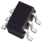
ICGOO电子元器件商城为您提供AD5247BKSZ5-RL7由Analog设计生产,在icgoo商城现货销售,并且可以通过原厂、代理商等渠道进行代购。 AD5247BKSZ5-RL7价格参考¥5.10-¥11.67。AnalogAD5247BKSZ5-RL7封装/规格:数据采集 - 数字电位器, Digital Potentiometer 5k Ohm 1 Circuit 128 Taps I²C Interface SC-70-6。您可以下载AD5247BKSZ5-RL7参考资料、Datasheet数据手册功能说明书,资料中有AD5247BKSZ5-RL7 详细功能的应用电路图电压和使用方法及教程。
AD5247BKSZ5-RL7 是由 Analog Devices Inc.(ADI)生产的一款数字电位器,属于数据采集系列中的数字电位器产品。其应用场景广泛,适用于需要可编程电阻调整的系统中。以下是该型号的主要应用场景:

1. 信号调节与增益控制
   AD5247 可用于放大器或滤波器电路中,作为可调分压器或增益控制器。通过数字接口调整电阻值,实现对信号幅度的动态控制,适用于音频设备、传感器信号调理等场景。

2. 电源管理
   在电源管理系统中,AD5247 可用作电压分压器,调节反馈网络以改变输出电压。例如,在 DC-DC 转换器或 LDO 中,通过数字控制实现动态电压调整。

3. 自动校准系统
   该器件支持非易失性存储器(EEPROM),可在断电后保存设置值。这使其非常适合需要自动校准的应用,如工业仪器、医疗设备和测试测量设备,能够补偿温度漂移或长期老化效应。

4. 用户界面调节
   在消费电子或工业设备中,AD5247 可用于实现用户可控的功能,例如音量调节、对比度/亮度调节或电机速度控制。通过 SPI 接口,微控制器可以轻松调整电位器值。

5. 滤波器调整
   数字电位器可用于有源滤波器设计中,动态调整滤波器的截止频率或品质因数(Q 值)。这种灵活性使得 AD5247 成为通信系统、音频处理和其他信号处理应用的理想选择。

6. 传感器接口与补偿
   在传感器信号链中,AD5247 可用于补偿传感器的非线性或温度变化引起的误差。通过调整电阻值,优化传感器的输出特性。

7. 便携式设备
   由于其低功耗特性和小型封装(SOT-23),AD5247 非常适合电池供电的便携式设备,如手持测量仪器、无线通信模块和健康监测设备。

总之,AD5247BKSZ5-RL7 的高精度、低功耗和非易失性特性,使其成为需要灵活电阻调整的各种应用的理想解决方案。
| 参数 | 数值 |
| 产品目录 | 集成电路 (IC) |
| 描述 | IC POT DGTL 5K 128POS SC70-6 |
| 产品分类 | |
| 品牌 | Analog Devices Inc |
| 数据手册 | |
| 产品图片 |
|
| 产品型号 | AD5247BKSZ5-RL7 |
| rohs | 无铅 / 符合限制有害物质指令(RoHS)规范要求 |
| 产品系列 | - |
| 供应商器件封装 | SC-70-6 |
| 其它名称 | AD5247BKSZ5-RL7DKR |
| 包装 | Digi-Reel® |
| 存储器类型 | 易失 |
| 安装类型 | 表面贴装 |
| 封装/外壳 | 6-TSSOP,SC-88,SOT-363 |
| 工作温度 | -40°C ~ 125°C |
| 抽头 | 128 |
| 接口 | I²C |
| 标准包装 | 1 |
| 温度系数 | 标准值 45 ppm/°C |
| 电压-电源 | 2.7 V ~ 5.5 V |
| 电路数 | 1 |
| 电阻(Ω) | 5k |
| 配用 | /product-detail/zh/AD5247EVAL/AD5247EVAL-ND/617335 |


- 商务部:美国ITC正式对集成电路等产品启动337调查
- 曝三星4nm工艺存在良率问题 高通将骁龙8 Gen1或转产台积电
- 太阳诱电将投资9.5亿元在常州建新厂生产MLCC 预计2023年完工
- 英特尔发布欧洲新工厂建设计划 深化IDM 2.0 战略
- 台积电先进制程称霸业界 有大客户加持明年业绩稳了
- 达到5530亿美元!SIA预计今年全球半导体销售额将创下新高
- 英特尔拟将自动驾驶子公司Mobileye上市 估值或超500亿美元
- 三星加码芯片和SET,合并消费电子和移动部门,撤换高东真等 CEO
- 三星电子宣布重大人事变动 还合并消费电子和移动部门
- 海关总署:前11个月进口集成电路产品价值2.52万亿元 增长14.8%


PDF Datasheet 数据手册内容提取
128-Position I2C-Compatible Digital Potentiometer Data Sheet AD5247 FEATURES FUNCTIONAL BLOCK DIAGRAM 128 positions VDD End-to-end resistance: 5 kΩ, 10 kΩ, 50 kΩ, 100 kΩ A Ultracompact, SC70-6 (2 mm × 2.1 mm) package SDA I2C-compatible interface I2C INTERFACE SCL Full read/write of wiper register W Power-on preset to midscale Single-supply 2.7 V to 5.5 V WIPER Rheostat mode temperature coefficient: 45 ppm/°C REGISTER B Low power, I = 0.9 µA at 3.3 V typical DD Wide operating temperature range: −40°C to +125°C GND 03876-001 APPLICATIONS Figure 1. Mechanical potentiometer replacement in new designs Transducer adjustment of pressure, temperature, position, chemical, and optical sensors RF amplifier-biasing LCD brightness and contrast adjustment Automotive electronics adjustment Gain control and offset adjustment have three hard-coded slave address options available to allow GENERAL DESCRIPTION users access to three of these devices on one I2C bus (see Table 8 for a full list of slave address locations). The AD5247 provides a compact, 2 mm × 2.1 mm, packaged solution for 128-position adjustment applications. This device The resistance between the wiper and either end point of performs the same electronic adjustment function as a mechanical the fixed resistor varies linearly with respect to the digital potentiometer or a variable resistor. Available in four different code transferred into the RDAC latch. Note the terms digital end-to-end resistance values (5 kΩ, 10 kΩ, 50 kΩ, and 100 kΩ), potentiometer, VR (variable resistor), and RDAC are used these low temperature coefficient devices are ideal for high interchangeably in this document. accuracy and stability variable resistance adjustments. Operating from a 2.7 V to 5.5 V power supply and consuming The wiper settings are controllable through the I2C-compatible 0.9 µA (3.3 V) allows the AD5247 to be used in portable digital interface, which can also be used to read back the present battery-operated applications. wiper register control word. The 10 kΩ and 100 kΩ options each Rev. F Information furnished by Analog Devices is believed to be accurate and reliable. However, no responsibility is assumed by Analog Devices for its use, nor for any infringements of patents or other One Technology Way, P.O. Box 9106, Norwood, MA 02062-9106, U.S.A. rights of third parties that may result from its use. Specifications subject to change without notice. No license is granted by implication or otherwise under any patent or patent rights of Analog Devices. Tel: 781.329.4700 www.analog.com Trademarks and registered trademarks are the property of their respective owners. Fax: 781.461.3113 ©2003–2012 Analog Devices, Inc. All rights reserved.
AD5247 Data Sheet TABLE OF CONTENTS Features .............................................................................................. 1 I2C Interface .................................................................................... 13 Applications ....................................................................................... 1 Theory of Operation ...................................................................... 14 Functional Block Diagram .............................................................. 1 Programming the Variable Resistor ......................................... 14 General Description ......................................................................... 1 Programming the Potentiometer Divider ............................... 15 Revision History ............................................................................... 2 I2C-Compatible 2-Wire Serial Bus ........................................... 15 Specifications ..................................................................................... 3 Level Shifting for Bidirectional Interface ................................ 16 Electrical Characteristics—5 kΩ Version .................................. 3 ESD Protection ........................................................................... 16 Electrical Characteristics—10 kΩ, 50 kΩ, and 100 kΩ Terminal Voltage Operating Range ......................................... 16 Versions .......................................................................................... 4 Maximum Operating Current .................................................. 16 Timing Characteristics—5 kΩ, 10 kΩ, 50 kΩ, and 100 kΩ Power-Up Sequence ................................................................... 16 Versions .......................................................................................... 5 Layout and Power Supply Bypassing ....................................... 17 Absolute Maximum Ratings ............................................................ 6 Constant Bias to Retain Resistance Setting ............................. 17 ESD Caution .................................................................................. 6 Outline Dimensions ....................................................................... 18 Pin Configuration and Function Descriptions ............................. 7 Ordering Guide .......................................................................... 18 Typical Performance Characteristics ............................................. 8 Test Circuits ..................................................................................... 12 REVISION HISTORY 5/12—Rev. E to Rev. F 3/07—Rev. A to Rev. B Changes to Features and General Description Sections .............. 1 Changes to General Description Section ....................................... 1 Changes to I Parameters, Table 1 ................................................ 3 Added Table 8 ................................................................................. 13 DD Changes to I Parameters, Table 2 ................................................ 4 Changes to I2C-Compatible 2-Wire Serial Bus Section ............ 15 DD Changes to Figure 15 ........................................................................ 9 Changes to Ordering Guide .......................................................... 18 Changes to Figure 16 ...................................................................... 10 7/06—Rev. 0 to Rev. A Removed Evaluation Board Section ............................................. 17 Updated Format .................................................................. Universal Changes to Ordering Guide .......................................................... 18 Changes to Absolute Maximum Ratings section .......................... 6 1/11—Rev. D to Rev. E Changes to Ordering Guide .......................................................... 18 Change to Table 1, Added Output Logic Low .............................. 3 9/03—Revision 0: Initial Version Change to Table 2, Added Output Logic Low .............................. 4 3/10—Rev. C to Rev. D Changes to Table 9 and Table 10 ................................................... 14 10/09—Rev. B to Rev. C Changes to Zero-Scale Error (10 kΩ) Parameter, Table 2 ........... 4 Changes to Ordering Guide .......................................................... 18 Rev. F | Page 2 of 20
Data Sheet AD5247 SPECIFICATIONS ELECTRICAL CHARACTERISTICS—5 kΩ VERSION V = 5 V ± 10% or 3 V ± 10%, V = V , −40°C < T < +125°C, unless otherwise noted. DD A DD A Table 1. Parameter Symbol Conditions Min Typ1 Max Unit DC CHARACTERISTICS—RHEOSTAT MODE Resistor Differential Nonlinearity2 R-DNL R , V = no connect −1.5 ±0.1 +1.5 LSB WB A Resistor Integral Nonlinearity2 R-INL R , V = no connect −4 ±0.75 +4 LSB WB A Nominal Resistor Tolerance3 ∆R −30 +30 % AB Resistance Temperature Coefficient3 ∆RAB/∆T 45 ppm/°C Output Resistance R Code = 0x00 75 300 Ω WB DC CHARACTERISTICS—POTENTIOMETER DIVIDER MODE Differential Nonlinearity4 DNL −1 ±0.1 +1 LSB Integral Nonlinearity4 INL −1 ±0.2 +1 LSB Voltage Divider Temperature Coefficient ∆V /∆T Code = 0x40 15 ppm/°C W Full-Scale Error V Code = 0x7F −3 −2 0 LSB WFSE Zero-Scale Error V Code = 0x00 0 1 2 LSB WZSE RESISTOR TERMINALS Voltage Range5 V V GND V V A, W DD Capacitance A6 C f = 1 MHz, measured to GND, A code = 0x40 45 pF Capacitance W6 C f = 1 MHz, measured to GND, W code = 0x40 60 pF Common-Mode Leakage I V = V /2 1 nA CM A DD DIGITAL INPUTS AND OUTPUTS Input Logic High V V = 5 V 2.4 V IH DD Input Logic Low V V = 5 V 0.8 V IL DD Input Logic High V V = 3 V 2.1 V IH DD Input Logic Low V V = 3 V 0.6 V IL DD Input Current I V = 0 V or 5 V ±1 μA IL IN Input Capacitance6 C 5 pF IL Output Logic Low (SDA) V I = 3 mA 0.4 V OL OL I = 6 mA 0.6 V OL POWER SUPPLIES Power Supply Range V 2.7 5.5 V DD RANGE Supply Current I V = 5.5 V; V = V or V = GND 3 7 μA DD DD IH DD IL V = 5 V; V = V or V = GND 2.5 5.2 μA DD IH DD IL V = 3.3 V; V = V or V = GND 0.9 2 μA DD IH DD IL Power Dissipation7 P V = 5 V or V = 0 V, V = 5 V 40 μW DISS IH IL DD Power Supply Sensitivity PSSR V = 5 V ± 10%, DD code = midscale ±0.003 ±0.05 %/% DYNAMIC CHARACTERISTICS6, 8 Bandwidth –3 dB BW_5 K R = 5 kΩ, code = 0x40 1.2 MHz AB Total Harmonic Distortion THD V = 1 V rms, V = 0 V, f = 1 kHz 0.05 % W A B V Settling Time t V = 5 V, ±1 LSB error band 1 μs W S A Resistor Noise Voltage Density e R = 2.5 kΩ, R = 0 Ω 6 nV/√Hz N_WB WB S 1 Typical specifications represent average readings at 25°C and VDD = 5 V. 2 Resistor position nonlinearity error R-INL is the deviation from an ideal value measured between the maximum resistance and the minimum resistance wiper positions. R-DNL measures the relative step change from ideal between successive tap positions. Parts are guaranteed monotonic. 3 VA = VDD, wiper (VW) = no connect. 4 INL and DNL are measured at VW, with the RDAC configured as a potentiometer divider similar to a voltage output DAC. VA = VDD and VB = 0 V. DNL specification limits of ±1 LSB maximum are guaranteed monotonic under operating conditions. 5 Resistor Terminal A and Resistor Terminal W have no limitations on polarity with respect to each other. 6 Guaranteed by design and not subject to production test. 7 PDISS is calculated from (IDD × VDD). CMOS logic level inputs result in minimum power dissipation. 8 All dynamic characteristics use VDD = 5 V. Rev. F | Page 3 of 20
AD5247 Data Sheet ELECTRICAL CHARACTERISTICS—10 kΩ, 50 kΩ, AND 100 kΩ VERSIONS V = 5 V ± 10% or 3 V ± 10%, V = V , −40°C < T < +125°C, unless otherwise noted. DD A DD A Table 2. Parameter Symbol Conditions Min Typ1 Max Unit DC CHARACTERISTICS—RHEOSTAT MODE Resistor Differential Nonlinearity2 R-DNL R , V = no connect −1 ±0.1 +1 LSB WB A Resistor Integral Nonlinearity2 R-INL R , V = no connect −2 ±0.25 +2 LSB WB A Nominal Resistor Tolerance3 ∆R −20 +20 % AB Resistance Temperature Coefficient3 ∆RAB/∆T 45 ppm/°C Output Resistance R Code = 0x00 75 300 Ω WB DC CHARACTERISTICS—POTENTIOMETER DIVIDER MODE Differential Nonlinearity4 DNL −1 ±0.1 +1 LSB Integral Nonlinearity4 INL −1 ±0.2 +1 LSB Voltage Divider Temperature Coefficient ∆V /∆T Code = 0x40 15 ppm/°C W Full-Scale Error (50 kΩ, 100 kΩ) V Code = 0x7F −1 −1 0 LSB WFSE Zero-Scale Error (50 kΩ, 100 kΩ) V Code = 0x00 0 0.4 1 LSB WZSE Full-Scale Error (10 kΩ) V Code = 0x7F −2 −0.5 0 LSB WFSE Zero-Scale Error (10 kΩ) V V = 4.5 V to 5.5 V, code = 0x00 0 0.5 1 LSB WZSE DD V = 2.7 V to 4.4 V, code = 0x00 0 0.5 1.2 LSB DD RESISTOR TERMINALS Voltage Range5 V V GND V V A, W DD Capacitance A6 C f = 1 MHz, measured to GND, A code = 0x40 45 pF Capacitance W6 C f = 1 MHz, measured to GND, W code = 0x40 60 pF Common-Mode Leakage I V = V /2 1 nA CM A DD DIGITAL INPUTS AND OUTPUTS Input Logic High V V = 5 V 2.4 V IH DD Input Logic Low V V = 5 V 0.8 V IL DD Input Logic High V V = 3 V 2.1 V IH DD Input Logic Low V V = 3 V 0.6 V IL DD Input Current I V = 0 V or 5 V ±1 µA IL IN Input Capacitance6 C 5 pF IL Output Logic Low (SDA) V I = 3 mA 0.4 V OL OL I = 6 mA 0.6 V OL POWER SUPPLIES Power Supply Range V 2.7 5.5 V DD RANGE Supply Current I V = 5.5 V; V = V or V = GND 3 7 µA DD DD IH DD IL V = 5 V; V = V or V = GND 2.5 5.2 µA DD IH DD IL V = 3.3 V; V = V or V = GND 0.9 2 µA DD IH DD IL Power Dissipation7 P V = 5 V or V = 0 V, V = 5 V 40 µW DISS IH IL DD Power Supply Sensitivity PSSR V = 5 V ± 10%, code = midscale ±0.01 ±0.02 %/% DD Rev. F | Page 4 of 20
Data Sheet AD5247 Parameter Symbol Conditions Min Typ1 Max Unit DYNAMIC CHARACTERISTICS6, 8 Bandwidth –3 dB BW R = 10 kΩ/50 kΩ/100 kΩ, 600/100/40 AB code = 0x40 kHz Total Harmonic Distortion THD V =1 V rms, f = 1 kHz, R = 10 kΩ 0.05 % W A AB V Settling Time (10 kΩ/50 kΩ/100 kΩ) t V = 5 V ±1 LSB error band 2 µs W S A Resistor Noise Voltage Density e R = 5 kΩ, R = 0 9 nV/√Hz N_WB WB S 1 Typical specifications represent average readings at 25°C and VDD = 5 V. 2 Resistor position nonlinearity error R-INL is the deviation from an ideal value measured between the maximum resistance and the minimum resistance wiper positions. R-DNL measures the relative step change from ideal between successive tap positions. Parts are guaranteed monotonic. 3 VA = VDD, wiper (VW) = no connect. 4 INL and DNL are measured at VW, with the RDAC configured as a potentiometer divider similar to a voltage output DAC. VA = VDD and VB = 0 V. DNL specification limits of ±1 LSB maximum are guaranteed monotonic operating conditions. 5 Resistor Terminal A and Resistor Terminal W have no limitations on polarity with respect to each other. 6 Guaranteed by design, not subject to production test. 7 PDISS is calculated from (IDD × VDD). CMOS logic level inputs result in minimum power dissipation. 8 All dynamic characteristics use VDD = 5 V. TIMING CHARACTERISTICS—5 kΩ, 10 kΩ, 50 kΩ, AND 100 kΩ VERSIONS V = 5 V ± 10% or 3 V ± 10%, V = V , −40°C < T < +125°C, unless otherwise noted. DD A DD A Table 3. Parameter1, 2, 3 Symbol Min Typ4 Max Unit SCL Clock Frequency f 400 kHz SCL Bus Free Time Between Stop and Start, t t 1.3 µs BUF 1 Hold Time (Repeated Start), t 5 t 0.6 µs HD;STA 2 Low Period of SCL Clock, t t 1.3 µs LOW 3 High Period of SCL Clock, t t 0.6 50 µs HIGH 4 Setup Time for Repeated Start Condition, t t 0.6 µs SU;STA 5 Data Hold Time, t t 0.9 µs HD;DAT 6 Data Setup Time, t t 100 ns SU;DAT 7 Fall Time of Both SDA and SCL Signals, t t 300 ns F 8 Rise Time of Both SDA and SCL Signals, t t 300 ns R 9 Setup Time for Stop Condition, t t 0.6 µs SU;STO 10 1 Specifications apply to all parts. 2 Guaranteed by design, not subject to production test. 3 See timing diagrams (Figure 2, Figure 33, and Figure 34) for locations of measured values. 4 Typical specifications represent average readings at 25°C and VDD = 5 V. 5 After this period, the first clock pulse is generated. t8 t9 t2 SCL t6 t5 t2 t3 t9 t4 t7 t10 t8 SDA P t1 S S P 03876-031 Figure 2. I2C Interface, Detailed Timing Diagram Rev. F | Page 5 of 20
AD5247 Data Sheet ABSOLUTE MAXIMUM RATINGS T = 25°C, unless otherwise noted. A Stresses above those listed under Absolute Maximum Ratings may cause permanent damage to the device. This is a stress Table 4. rating only; functional operation of the device at these or any Parameter Rating other conditions above those indicated in the operational V to GND –0.3 V to +7 V DD section of this specification is not implied. Exposure to absolute V , V to GND V A W DD maximum rating conditions for extended periods may affect Terminal Current, Ax to Bx, Ax to Wx, Bx to Wx device reliability. Pulsed1 ±20 mA Continuous ±5 mA ESD CAUTION Digital Inputs and Output Voltage to GND 0 V to V + 0.3 V DD Operating Temperature Range –40°C to +125°C Maximum Junction Temperature (T ) 150°C JMAX Storage Temperature Range –65°C to +150°C Thermal Resistance θ 2: (SC70-6) 340°C/W JA Reflow Soldering Peak Temperature SnPb 240°C Pb-Free 260°C 1 Maximum terminal current is bounded by the maximum current handling of the switches, maximum power dissipation of the package, and maximum applied voltage across any two of the A, B, and W terminals at a given resistance. 2 Package power dissipation = (TJMAX – TA)/θJA. Rev. F | Page 6 of 20
Data Sheet AD5247 PIN CONFIGURATION AND FUNCTION DESCRIPTIONS VDD 1 6 A AD5247 GND 2 TOPVIEW 5 W (NottoScale) SCL 3 4 SDA 03876-043 Figure 3. Pin Configuration Table 5. Pin Function Descriptions Pin No. Mnemonic Description 1 V Positive Power Supply. DD 2 GND Digital Ground and B Termination Voltage. 3 SCL Serial Clock Input; Positive Edge Triggered. 4 SDA Serial Data Input/Output. 5 W Terminal W. 6 A Terminal A. Rev. F | Page 7 of 20
AD5247 Data Sheet TYPICAL PERFORMANCE CHARACTERISTICS 1.0 0.25 0.8 RTAAB==251°0CkΩ 0.20 –+4205°°CC VRDADB==21.07kVΩ E INL (LSB)E INL (LSB) 000...264 VDD=2.7V ODE DNL (LSB) 000...011505 ++81525°C°C TA=–40°C,+25°C,+85°C,+125°C AT MODAT MOD –0.20 VDD=5.5V ETER M–0.050 TT M RHEOSRHEOS ––00..46 TENTIO––00..1150 O ––01..08 03876-002 P––00..2250 03876-005 0 16 32 48 64 80 96 112 128 0 16 32 48 64 80 96 112 128 CODE(Decimal) CODE(Decimal) Figure 4. R-INL vs. Code vs. Supply Voltages Figure 7. DNL vs. Code vs. Temperature 0.5 0.25 00..34 RTAAB==251°0CkΩ SB) 00..2105 TRAAB==251°0CkΩ DNL (LSB) 00..12 VDD=2.7V ODE INL (L 00..0150 VDD=2.7V E M OD 0 ER 0 M T OSTAT ––00..21 VDD=5.5V NTIOME––00..1005 VDD=5.5V E E H T R –0.3 O–0.15 P ––00..54 03876-003 ––00..2205 03876-006 0 16 32 48 64 80 96 112 128 0 16 32 48 64 80 96 112 128 CODE(Decimal) CODE(Decimal) Figure 5. R-DNL vs. Code vs. Supply Voltages Figure 8. INL vs. Code vs. Supply Voltages 0.25 0.25 ODE INL (LSB) 0000....01215005 TTTTAAAA====–+++42810552°5°°CCC°C TA=+25°C,+85°CVR,+DA1DB2==5°21C.07kVΩ ODE DNL (LSB) 0000....01215005 VVDDDDV==DD25..=75VV2.7V TRAAB==251°0CkΩ M M R 0 R 0 E E T T ME–0.05 ME–0.05 NTIO–0.10 TA=–40°C NTIO–0.10 VDD=5.5V E E OT–0.15 OT–0.15 P P ––00..2250 03876-004 ––00..2205 03876-007 0 16 32 48 64 80 96 112 128 0 16 32 48 64 80 96 112 128 CODE(Decimal) CODE(Decimal) Figure 6. INL vs. Code vs. Temperature Figure 9. DNL vs. Code vs. Supply Voltages Rev. F | Page 8 of 20
Data Sheet AD5247 1.0 1.50 0.8 TA=–40°C TA=+85°C 1.25 0.6 B) B) S 0.4 S MODE INL (L 0.20 TA=+25°C TA=+125°C E ERROR (L 01..0705 VDD = 5.5V, VA = 5.5V AT –0.2 CAL OST –0.4 O-S 0.50 HE TA=–40°C ER R –0.6 TA=+25°C Z ––10..08 TTAA==++81255°C°C 03876-008 0.250 VDD = 2.7V, VA = 2.7V 03876-011 0 16 32 48 64 80 96 112 128 –40 –25 –10 5 20 35 50 65 80 95 110 125 CODE(Decimal) TEMPERATURE (°C) Figure 10. R-INL vs. Code vs. Temperature Figure 13. Zero-Scale Error vs. Temperature 0.5 100 0.4 +–4205°°CC VRDADB==21.07kVΩ DCIOGDITEA=L 0IxN4P0UTS=0V E DNL (LSB) 000...123 ++81525°C°C TA=–40°C,+25°C,+85°C,+125°C RENT (µA) 10 VDD=5.5V D R O 0 U 1 M C EOSTAT ––00..12 SUPPLY VDD=2.7V H D, 0.1 R –0.3 ID ––00..54 03876-009 0.01 03876-012 0 16 32 48 64 80 96 112 128 –40 –25 –10 5 20 35 50 65 80 95 110 125 CODE(Decimal) TEMPERATURE(°C) Figure 11. R-DNL vs. Code vs. Temperature Figure 14. Supply Current vs. Temperature 0 100 5V 2.7V C) 90 NL (LSB)OR (LSB)––10..05 VDD = 5.5V, VA = 5.5V MPCO (ppm/° 678000 E IRR TE ODE E–1.5 DE 50 ML O EOSTAT ULL-SCA –2.0 VDD = 2.7V, VA = 2.7V OSTAT M 3400 HF S R E 20 –2.5 TH –3.0–40 –25 –10 5 T2E0MPE3R5ATU5R0E (°6C5) 80 95 110 12503876-010 R 1001IRWAB9B == 1 217000kµ2ΩA5 33 41 4C9O5D7E (6D5ec7im3al8)1 89 97 105113121 03876-013 Figure 12. Full-Scale Error vs. Temperature Figure 15. ∆RWB/∆T vs. Code Rev. F | Page 9 of 20
AD5247 Data Sheet 100 0 2.7V C) 80 5V –6 0x40 m/° 0x20 pp 60 –12 O ( 0x10 C 40 –18 P M 0x08 TE 20 B) –24 R MODE –200 GAIN (d ––3306 00xx0042 E T 0x01 ME –40 –42 O NTI –60 –48 E POT–1–08001 10 19 28 37 46CO55DE6 (4Dec7i3mal8)2 91 100VR1AA0 B=9 =V1 D1180Dk1Ω27 03876-014 ––56401k 10k FREQU1E00NkCY(Hz) 1M 10M03876-017 Figure 16. ∆VWB/∆T vs. Code Figure 19. Gain vs. Frequency vs. Code, RAB = 50 kΩ 0 0 0x40 0x40 –6 –6 0x20 0x20 –12 –12 0x10 0x10 –18 –18 0x08 0x08 AIN (dB) ––2340 00xx0042 AIN (dB) ––2340 0x04 G –36 0x01 G –36 0x02 0x01 –42 –42 –48 –48 ––6504 03876-015 ––5640 03876-018 1k 10k 100k 1M 10M 1k 10k 100k 1M 10M FREQUENCY(Hz) FREQUENCY(Hz) Figure 17. Gain vs. Frequency vs. Code, RAB = 5 kΩ Figure 20. Gain vs. Frequency vs. Code, RAB = 100 kΩ 0 0 0x40 –6 –6 5kΩ 0x20 –12 –12 10kΩ 0x10 –18 –18 100kΩ 0x08 50kΩ B) –24 B) –24 N (d –30 0x04 N (d –30 AI 0x02 AI G G –36 –36 0x01 –42 –42 –48 –48 ––5640 03876-016 ––6504 03876-019 1k 10k 100k 1M 10M 1k 10k 100k 1M 10M FREQUENCY(Hz) FREQUENCY(Hz) Figure 18. Gain vs. Frequency vs. Code, RAB = 10 kΩ Figure 21. −3 dB Bandwidth @ Code = 0x80 Rev. F | Page 10 of 20
Data Sheet AD5247 0.30 A - VCDODD =E 5=. 50Vx55 TA= 25°C VVVDABD == =50 .V50.V5V RTAA B= =2 51°0CkΩ 0.25 B-VDD = 5.5V CODE 0x40 TO CODE 0x3F CODE = 0x7F 0.20 C-VDD = 2.7V CODE = 0x55 A) (µD 0.15 D-VDD = 2.7V D CODE = 0x7F I VW 0.10 A B 0.05 0 CD 03876-020 03876-023 1k 10k 100k 1M 200ns/DIV FREQUENCY (Hz) Figure 22. IDD vs. Frequency Figure 25. Midscale Glitch, Code 0x40 to Code 0x3F 150 TRAAB==255°0CkΩ VVDAD = =5 .50.V5V TRAA B= =2 51°0CkΩ 125 VB = 0V CODE 0x00 TO CODE 0x7F Ω) E ( 100 C TAN VDD=2.7V VW SIS 75 E R R PE 50 WI 250 VDD=5.5V 03876-021 03876-024 0 16 32 48 64 80 96 112 128 4µs/DIV CODE(Decimal) Figure 23. Wiper Resistance vs. Code vs. VDD Figure 26. Large Signal Settling Time VDD=5.5V TA=25°C VA=5.0V RAB=10kΩ VB=0V FCLK=100kHz VW 5V CLK 0V 03876-022 1µs/DIV Figure 24. Digital Feedthrough Rev. F | Page 11 of 20
AD5247 Data Sheet TEST CIRCUITS Figure 27 to Figure 32 define the test conditions used in the Specifications section. VA V+ = VDD ± 10% V+ ADUTW V1L+S=BV=DDV+/2N V+ VDD ADUWT PSSR (%/%) =ΔΔVVMDDS%% B B VMS 03876-025 VMS 03876-028 Figure 27. Potentiometer Divider Nonlinearity Error (INL, DNL) Figure 30. Power Supply Sensitivity (PSS, PSSR) NOCONNECT DUT DUT A IW A +15V W VIN W B VMS B OP27 VOUT 03876-026 –15V 03876-029 Figure 28. Resistor Position Nonlinearity Error (R-INL, R-DNL) Figure 31. Gain vs. Frequency NC DUT DUT VMS2 A W VW IW=VDD/RNOMINAL VDD A W ICM B VMS1 RW=[VMS1–VMS2]/IW 03876-027 GNDNCB VCM 03876-030 Figure 29. Wiper Resistance Figure 32. Common-Mode Leakage Current Rev. F | Page 12 of 20
Data Sheet AD5247 I2C INTERFACE The following abbreviations are used in this section: • S = start condition • W = write • P = stop condition • R = read • A = acknowledge • A6, A5, A4, A3, A2, A1, A0 = address bits • X = don’t care • D6, D5, D4, D3, D2, D1, D0 = data bits Table 6. Write Mode S A6 A5 A4 A3 A2 A1 A0 W A X D6 D5 D4 D3 D2 D1 D0 A P Slave Address Byte Data Byte Table 7. Read Mode S A6 A5 A4 A3 A2 A1 A0 R A 0 D6 D5 D4 D3 D2 D1 D0 A P Slave Address Byte Data Byte 1 9 1 9 1 SCL SDA A6 A5 A4 A3 A2 A1 A0 R/W X D6 D5 D4 D3 D2 D1 D0 ACK ACK BY ACK BY STMAARSTT EBRY SLAVE FARDADMREE S1S BYTE AD5247 DFARTAAMBEYT2E AD5247 SMTAOSPT EBRY 03876-032 Figure 33. Writing to the RDAC Register 1 9 1 9 SCL S A6 A5 A4 A3 A2 A1 A0 R/W 0 D6 D5 D4 D3 D2 D1 D0 ACK BY NOACKBY STMAARSTT EBRY SLAVE FARDADMREE S1S BYTE AD5247 RDAFCR RAEMGEI S2TER MASTER SMTAOSPTEBRY 03876-033 Figure 34. Reading from the RDAC Register Table 8. I2C Slave Addresses Slave Addresses Slave Address Model A6 A5 A4 A3 A2 A1 A0 Model A6 A5 A4 A3 A2 A1 A0 AD5247BKS5-R2 0 1 0 1 1 1 0 AD5247BKS50-RL7 0 1 0 1 1 1 0 AD5247BKS5-RL7 0 1 0 1 1 1 0 AD5247BKSZ50-RL7 0 1 0 1 1 1 0 AD5247BKSZ5-RL7 0 1 0 1 1 1 0 AD5247BKS100-R2 0 1 0 1 1 1 0 AD5247BKS10-R2 0 1 0 1 1 1 0 AD5247BKSZ100-R2 0 1 0 1 1 1 0 AD5247BKS10-RL7 0 1 0 1 1 1 0 AD5247BKS100-RL7 0 1 0 1 1 1 0 AD5247BKSZ10-RL7 0 1 0 1 1 1 0 AD5247BKSZ100-RL7 0 1 0 1 1 1 0 AD5247BKSZ10-1RL7 0 0 1 0 1 1 1 AD5247BKSZ100-1RL7 0 0 1 0 1 1 1 AD5247BKSZ10-2RL7 0 0 1 0 1 1 0 AD5247BKSZ100-2RL7 0 0 1 0 1 1 0 AD5247BKS50-R2 0 1 0 1 1 1 0 Rev. F | Page 13 of 20
AD5247 Data Sheet THEORY OF OPERATION The AD5247 is a 128-position, digitally-controlled variable The general equation determining the digitally programmed resistor (VR) device. An internal power-on preset places the output resistance between W and B is wiper at midscale during power-on, which simplifies the D default condition recovery at power-up. RWB(D)=128×RAB +2×RW (1) PROGRAMMING THE VARIABLE RESISTOR where: Rheostat Operation D is the decimal equivalent of the binary code loaded in the The nominal resistance (R ) of the RDAC between Terminal A 7-bit RDAC register. AB and Terminal B is available in 5 kΩ, 10 kΩ, 50 kΩ, and 100 kΩ. The RAB is the end-to-end resistance. final two or three digits of the part number determine the nominal RW is the wiper resistance contributed by the on resistance of resistance value; for example, 10 kΩ = 10 and 50 kΩ = 50. The the internal switch. RAB of the VR has 128 contact points accessed by the wiper In summary, if RAB = 10 kΩ and the Terminal A is open-circuited, terminal, plus the B terminal contact. The 7-bit data in the the output resistance R , shown in Table 9, is set for the indicated WB RDAC latch is decoded to select one of the 128 possible settings. RDAC latch codes. Assuming a 10 kΩ part is used, the wiper’s first connection starts Table 9. Codes and Corresponding R Resistance WB at the B terminal for Data 0x00. Because there is a 50 Ω wiper D (Decimal) R (Ω) Output State contact resistance, such a connection yields a minimum of 100 Ω WB 127 10,072 Full scale (R + 2 × R ) (2 × 50 Ω) resistance between Terminal W and Terminal B. The AB W 64 5150 Midscale second connection is the first tap point, corresponding to 178 Ω 1 228 1 LSB (R = R /128 + R = 78 Ω + 2 × 50 Ω) for Data 0x01. The third WB AB W 0 150 Zero scale (wiper contact resistance) connection is the next tap point, representing 256 Ω (2 × 78 Ω + 2 × 50 Ω) for Data 0x02, and so on. Each LSB data value increase Note that in the zero-scale condition, a finite resistance of moves the wiper up the resistor ladder until the last tap point is 100 Ω between Terminal W and Terminal B is present. Care reached at 10,100 Ω (R + 2 × R ). should be taken to limit the current flow between W and B in AB W this state to a maximum pulse current of no more than 20 mA. Figure 35 shows a simplified diagram of the equivalent RDAC Otherwise, degradation or possible destruction of the internal circuit where the last resistor string is not accessed. switch contact can occur. Ax Similar to the mechanical potentiometer, the resistance of the RDAC between Wiper W and Terminal A also produces a digitally controlled complementary resistance, R . When WA DD65 RS these terminals are used, the Terminal B can be opened. Set the D4 DD23 RS resistance value for RWA to start at a maximum value of resistance D1 and to decrease the data loaded in the latch increases in value. D0 Wx The general equation for this operation is RDAC R (D)=128−D×R +2×R (2) LATCH WA 128 AB W DECAONDDER RS Bx If R = 10 kΩ and the B terminal is open-circuited, the output AB 03876-034 lraetscihst acnocdee,s R. WA, shown in Table 10, is set for the indicated RDAC Figure 35. AD5247 Equivalent RDAC Circuit Table 10. Codes and Corresponding R Resistance WA D (Decimal) R (Ω) Output State WA 127 228 Full scale 64 5150 Midscale 1 10,071 1 LSB 0 10,150 Zero scale Typical device-to-device matching is process lot dependent and can vary by up to ±30%. Because the resistance element is processed in thin film technology, the change in R with AB temperature has a very low 45 ppm/°C temperature coefficient. Rev. F | Page 14 of 20
Data Sheet AD5247 PROGRAMMING THE POTENTIOMETER DIVIDER The 2-wire I2C serial bus protocol operates as follows: Voltage Output Operation 1. The master initiates a data transfer by establishing a start The digital potentiometer easily generates a voltage divider at condition, which is when a high-to-low transition on the wiper-to-B and wiper-to-A, proportional to the input voltage SDA line occurs while SCL is high (see Figure 33). The at A-to-B. Unlike the polarity of V to GND, which must be following byte is the slave address byte, consisting of the DD positive, voltage across A-to-B, W-to-A, and W-to-B can be at 7-bit slave address followed by an R/W bit (this bit determines either polarity. whether data is read from or written to the slave device). The slave, whose address corresponds to the transmitted address, If ignoring the effect of the wiper resistance for approximation, responds by pulling the SDA line low during the ninth clock connecting the Terminal A to 5 V and the Terminal B to ground pulse (this is termed the acknowledge bit). At this stage, all produces an output voltage at the wiper-to-B starting at 0 V up other devices on the bus remain idle while the selected to 1 LSB less than 5 V. Each LSB of voltage is equal to the voltage device waits for data to be written to or read from its serial applied across Terminal A and Terminal B divided by the 128 register. If the R/W bit is high, the master reads from the positions of the potentiometer divider. The general equation slave device. If the R/W bit is low, the master writes to the defining the output voltage at V with respect to ground for any W slave device. valid input voltage applied to Terminal A and Terminal B is 2. In write mode, after acknowledgement of the slave address D VW(D)=128×VA (3) byte, the next byte is the data byte. Data is transmitted over the serial bus in sequences of nine clock pulses (eight data A more accurate calculation that includes the effect of wiper bits followed by an acknowledge bit). The transitions on resistance, V , is W the SDA line must occur during the low period of SCL R (D) and remain stable during the high period of SCL (see V (D)= WB ×V (4) W R A Figure 33). AB 3. In read mode, after acknowledgment of the slave address Operation of the digital potentiometer in the divider mode byte, data is received over the serial bus in sequences of results in a more accurate operation over temperature. Unlike nine clock pulses (a slight difference from write mode, rheostat mode, divider mode makes the output voltage mainly on where eight data bits are followed by an acknowledge bit). the ratio of Internal Resistor R to Internal Resistor R , and WA WB Similarly, the transitions on the SDA line must occur not the absolute values. Therefore, the temperature drift reduces during the low period of SCL and remain stable during to 15 ppm/°C. the high period of SCL (see Figure 34). I2C-COMPATIBLE 2-WIRE SERIAL BUS 4. When all data bits have been read or written, a stop con- The first byte of the AD5247 is a slave address byte (see the I2C dition is established by the master. A stop condition is Interface section). It has a 7-bit slave address and an R/W bit. defined as a low-to-high transition on the SDA line while The 5 kΩ and 50 kΩ options support one 7-bit slave address SCL is high. In write mode, the master pulls the SDA line while the 10 kΩ and 100 kΩ options each have three hard-coded high during the 10th clock pulse to establish a stop condition slave address options available (see Table 8 for a full list of slave (see Figure 33). In read mode, the master issues a no address locations). The extra hard coded slave addresses on the acknowledge for the ninth clock pulse (that is, the SDA 10 kΩ and 100 kΩ options allow users to employ up to three of line remains high). The master then brings the SDA line these devices on one I2C bus. The seven MSBs of the slave address low before the 10th clock pulse, which goes high to establish are followed by 0 for a write command or 1 to place the device a stop condition (see Figure 34). in read mode. A repeated write function gives the user flexibility to update the RDAC output a number of times after addressing the part only once. For example, after the RDAC has acknowledged its slave address in the write mode, the RDAC output updates on each successive byte. If different instructions are needed, the write/read mode has to start again with a new slave address and data byte. Similarly, a repeated read function of the RDAC is also allowed. Rev. F | Page 15 of 20
AD5247 Data Sheet LEVEL SHIFTING FOR BIDIRECTIONAL INTERFACE MAXIMUM OPERATING CURRENT While most legacy systems can be operated at one voltage, a At low code values, the user should be aware that, due to low new component can be optimized at another voltage. When resistance values, the current through the RDAC might exceed two systems operate the same signal at two different voltages, the 5 mA limit. In Figure 39, a 5 V supply is placed on the wiper, proper level shifting is needed. For instance, users can employ and the current through Terminal W and Terminal B is plotted a 3.3 V E2PROM to interface with a 5 V digital potentiometer. A with respect to code. A line is also drawn denoting the 5 mA level shifting scheme is needed to enable a bidirectional commu- current limit. Note that at low code values (particularly for the nication so that the setting of the digital potentiometer can be 5 kΩ and 10 kΩ options), the current level increases signifi- stored in and retrieved from the E2PROM. Figure 36 shows one cantly. Care should be taken to limit the current flow between of the level-shifting implementations. M1 and M2 can be any W and B in this state to a maximum continuous current of N-channel signal FETs, or if V falls below 2.5 V, M1 and M2 5 mA and a maximum pulse current of no more than 20 mA. DD can be low threshold FETs such as the FDV301N. Otherwise, degradation or possible destruction of the internal VDD1=3.3V VDD2=5V switch contacts can occur. 100 RP RP RP RP G S D SDA1 SDA2 10 G 5mA CURRENT LIMIT M1 S D A) SCL1 SCL2 m T ( RAB= 5kΩ M2 N 3.3V 5V E 1 R R E2PROM AD5247 03876-035 I CUWB RAB= 10kΩRAB= 50kΩ Figure 36. Level-Shifting for Operation at Different Potentials 0.1 EASll Ddi gPitRalO inTpEutCs TarIeO pNro tected with a series input resistor and 0.01 RAB= 100kΩ 03876-039 0 16 32 48 64 80 96 112 128 parallel Zener ESD structures as shown in Figure 37. This applies CODE (Decimal) to digital input pins (SDA and SCL). Figure 39. Maximum Operating Current SDA/ 340Ω LOGIC POWER-UP SEQUENCE SCL Because the ESD protection diodes limit the voltage compliance GND 03876-036 at Terminal A and Terminal W (see Figure 38), it is important to power V /GND before applying any voltage to Terminal A Figure 37. ESD Protection of Digital Pins DD and Terminal W; otherwise, the diode is forward-biased such TERMINAL VOLTAGE OPERATING RANGE that V is powered unintentionally and can affect the rest of the DD The AD5247 V and GND power supply defines the boundary user’s circuit. The ideal power-up sequence is in the following DD conditions for proper 3-terminal digital potentiometer operation. order: GND, VDD, digital inputs, VA, and VW. The relative order Supply signals present on Terminal A and Terminal W that exceed of powering VA and VW and the digital inputs is not important VDD or GND are clamped by the internal forward biased diodes as long as they are powered after VDD/GND. (see Figure 38). VDD A W GND 03876-038 Figure 38. Maximum Terminal Voltages Set by VDD and GND Rev. F | Page 16 of 20
Data Sheet AD5247 LAYOUT AND POWER SUPPLY BYPASSING AD5247. The measurement over time shows that the device draws approximately 1.3 µA and consumes negligible power. It is good practice to employ a compact, minimum lead-length Over a course of 30 days, the battery was depleted by less than layout design. The leads to the inputs should be as direct as pos- 2%, the majority of which was due to the intrinsic leakage sible with minimum conductor length. Ground paths should current of the battery itself. have low resistance and low inductance. 110% Similarly, it is good practice to bypass the power supplies with 108% quality capacitors for optimum stability. Supply leads to the device TA=25°C 106% should be bypassed with 0.01 µF to 0.1 µF disc or chip ceramic D capacitors. Low ESR 1 µF to 10 µF tantalum or electrolytic capaci- TE104% E tors should also be applied at the supplies to minimize any transient PL102% E disturbance and low frequency ripple (see Figure 40). Note that the E D100% F digital ground should also be joined remotely to the analog ground LI Y 98% at one point to minimize the ground bounce. ER TT 96% A B 94% VDD VDD 10CµF3 + 0.1CµF1 AD5247 9902%% 03876-041 0 5 10 15 20 25 30 DAYS Figure 41. Battery Operating Life Depletion GND 03876-040 Tish ai sp draecmtiocanls tarpapteros athchat. Mcoonsstt apnotrlyta bbilaes dinegv itchees pdoot nenotti oremquetierer Figure 40. Power Supply Bypassing the removal of batteries for charging. Although the resistance CONSTANT BIAS TO RETAIN RESISTANCE SETTING setting of the AD5247 is lost when the battery needs replace- ment, such events occur rather infrequently. As a result, this For users who desire nonvolatility but cannot justify the additional inconvenience is justified by the lower cost and smaller size cost for the EEMEM, the AD5247 can be considered a low cost offered by the AD5247. If total power is lost, the user should alternative because it maintains a constant bias to retain the be provided with a means to adjust the setting accordingly. wiper setting. The AD5247 is specifically designed with low power in mind, which allows low power consumption even in battery-operated systems. Figure 41 demonstrates the power consumption from a 3.4 V 450 mA/hr Li-Ion cell phone battery, which is connected to the Rev. F | Page 17 of 20
AD5247 Data Sheet OUTLINE DIMENSIONS 2.20 2.00 1.80 1.35 6 5 4 2.40 1.25 2.10 1.15 1 2 3 1.80 0.65BSC 1.30BSC 1.00 1.10 0.40 0.90 0.80 0.10 0.70 0.46 0.10MAX 0.30 SPELAATNIENG 00..2028 0.36 COPLANARITY 0.15 0.26 0.10 COMPLIANTTOJEDECSTANDARDSMO-203-AB 072809-A Figure 42. 6-Lead Thin Shrink Small Outline Transistor Package [SC70] (KS-6) Dimensions shown in millimeters ORDERING GUIDE Package Model1 R (kΩ) Temperature Range Package Description2 Option Branding AB AD5247BKSZ5-RL7 5 –40°C to +125°C 6-lead Thin Shrink Small Outline Transistor Package [SC70] KS-6 D96 AD5247BKSZ10-RL7 10 –40°C to +125°C 6-lead Thin Shrink Small Outline Transistor Package [SC70] KS-6 D95 AD5247BKSZ10-1RL7 10 –40°C to +125°C 6-lead Thin Shrink Small Outline Transistor Package [SC70] KS-6 D5E AD5247BKSZ10-2RL7 10 –40°C to +125°C 6-lead Thin Shrink Small Outline Transistor Package [SC70] KS-6 DAK AD5247BKSZ50-RL7 50 –40°C to +125°C 6-lead Thin Shrink Small Outline Transistor Package [SC70] KS-6 D97 AD5247BKSZ100-R2 100 –40°C to +125°C 6-lead Thin Shrink Small Outline Transistor Package [SC70] KS-6 D98 AD5247BKSZ100-RL7 100 –40°C to +125°C 6-lead Thin Shrink Small Outline Transistor Package [SC70] KS-6 D98 AD5247BKSZ100-1RL7 100 –40°C to +125°C 6-lead Thin Shrink Small Outline Transistor Package [SC70] KS-6 DAJ AD5247BKSZ100-2RL7 100 –40°C to +125°C 6-lead Thin Shrink Small Outline Transistor Package [SC70] KS-6 DAL EVAL-AD5247DBZ Evaluation Board 1 Z = RoHS compliant part. 2 The evaluation board is shipped with the 10 kΩ RAB resistor option; however, the board is compatible with all available resistor value options. Rev. F | Page 18 of 20
Data Sheet AD5247 NOTES Rev. F | Page 19 of 20
AD5247 Data Sheet NOTES I2C refers to a communications protocol originally developed by Philips Semiconductors (now NXP Semiconductors). ©2003–2012 Analog Devices, Inc. All rights reserved. Trademarks and registered trademarks are the property of their respective owners. D03876-0-5/12(F) Rev. F | Page 20 of 20