ICGOO在线商城 > 集成电路(IC) > 数据采集 - 数字电位器 > AD5175BRMZ-10
 Datasheet下载
- 型号: AD5175BRMZ-10
- 制造商: Analog
- 库位|库存: xxxx|xxxx
- 要求:
| 数量阶梯 | 香港交货 | 国内含税 |
| +xxxx | $xxxx | ¥xxxx |
查看当月历史价格
查看今年历史价格
AD5175BRMZ-10产品简介:
ICGOO电子元器件商城为您提供AD5175BRMZ-10由Analog设计生产,在icgoo商城现货销售,并且可以通过原厂、代理商等渠道进行代购。 AD5175BRMZ-10价格参考¥16.82-¥30.82。AnalogAD5175BRMZ-10封装/规格:数据采集 - 数字电位器, Digital Potentiometer 10k Ohm 1 Circuit 1024 Taps I²C Interface 10-MSOP。您可以下载AD5175BRMZ-10参考资料、Datasheet数据手册功能说明书,资料中有AD5175BRMZ-10 详细功能的应用电路图电压和使用方法及教程。
AD5175BRMZ-10 是由 Analog Devices Inc.(ADI)生产的一款数字电位器,属于数据采集类产品。它是一种非易失性、低功耗的 CMOS 数字电位器,具有 256 级抽头分辨率和 EEPROM 存储功能,能够在断电后保存设置值。以下是该型号的一些典型应用场景:

 1. 可调增益放大器
   - AD5175BRMZ-10 可用于调整运算放大器的增益。通过改变电阻值,用户可以动态调节放大器的增益,适用于需要灵活增益控制的信号处理系统,例如音频设备、传感器信号调理电路等。

 2. 电压分压器
   - 在电源管理系统中,AD5175BRMZ-10 可用作电压分压器,用于生成参考电压或调节输出电压。其非易失性特性使得设置值在断电后仍然保留,适合需要稳定电压输出的应用。

 3. 传感器校准
   - 在工业自动化和测量仪器中,数字电位器可用于校准传感器输出。通过调整电阻值,可以补偿传感器的偏差或非线性误差,从而提高系统的精度。

 4. 滤波器调节
   - 在模拟滤波器设计中,AD5175BRMZ-10 可用于动态调节滤波器的截止频率或品质因数(Q 值)。这种灵活性使得它非常适合需要自适应滤波的应用场景。

 5. 音频音量控制
   - 在音频设备中,AD5175BRMZ-10 可以用作音量控制器。相比传统的机械电位器,数字电位器具有更高的可靠性和更长的使用寿命,同时支持远程控制。

 6. 电机控制
   - 在电机驱动电路中,AD5175BRMZ-10 可用于调节电机的启动电流或速度控制回路中的电阻值,从而实现精确的速度调节和能耗管理。

 7. 便携式设备中的电源管理
   - 由于其低功耗特性,AD5175BRMZ-10 非常适合用于电池供电的便携式设备中,例如医疗设备、手持仪表等。它可以动态调整电源电压或电流,以优化能效。

 8. 通信系统中的阻抗匹配
   - 在射频(RF)和通信系统中,AD5175BRMZ-10 可用于动态调整阻抗匹配网络,以优化信号传输效率和减少反射损耗。

 特点总结:
- 非易失性存储:断电后仍能保存设置值。
- 高分辨率:256 级抽头提供精细的调节能力。
- 低功耗:适合便携式和电池供电设备。
- 小型封装:节省空间,便于集成到紧凑型设计中。

这些特点使得 AD5175BRMZ-10 成为一种多功能且可靠的数字电位器,广泛应用于各种需要动态电阻调节的场景。
| 参数 | 数值 |
| 产品目录 | 集成电路 (IC)半导体 |
| 描述 | IC DGTL POT 1024POS 10K 10MSOP数字电位计 IC 1024-pos 5v Digital Rstat 50-TP Mem |
| 产品分类 | |
| 品牌 | Analog Devices Inc |
| 产品手册 | |
| 产品图片 |
|
| rohs | 符合RoHS无铅 / 符合限制有害物质指令(RoHS)规范要求 |
| 产品系列 | 数字电位计 IC,Analog Devices AD5175BRMZ-10- |
| 数据手册 | |
| 产品型号 | AD5175BRMZ-10 |
| POT数量 | Single |
| 产品种类 | 数字电位计 IC |
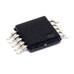
| 供应商器件封装 | 10-MSOP |
| 其它名称 | AD5175BRMZ10 |
| 包装 | 管件 |
| 商标 | Analog Devices |
| 存储器类型 | 非易失 |
| 安装类型 | 表面贴装 |
| 安装风格 | SMD/SMT |
| 容差 | 15 % |
| 封装 | Tube |
| 封装/外壳 | 10-TFSOP,10-MSOP(0.118",3.00mm 宽) |
| 封装/箱体 | MSOP-10 |
| 工作温度 | -40°C ~ 125°C |
| 工作电源电压 | 2.7 V |
| 工厂包装数量 | 50 |
| 弧刷存储器 | Non Volatile |
| 抽头 | 1024 |
| 接口 | I²C |
| 数字接口 | I2C |
| 最大工作温度 | + 125 C |
| 最小工作温度 | - 40 C |
| 标准包装 | 50 |
| 每POT分接头 | 1024 |
| 温度系数 | 标准值 35 ppm/°C |
| 电压-电源 | 2.7 V ~ 5.5 V, ±2.5 V ~ 2.75 V |
| 电源电压-最大 | 5.5 V |
| 电源电压-最小 | 2.7 V |
| 电源电流 | 0.3 uA |
| 电路数 | 1 |
| 电阻 | 10 kOhms |
| 电阻(Ω) | 10k |
| 系列 | AD5175 |


- 商务部:美国ITC正式对集成电路等产品启动337调查
- 曝三星4nm工艺存在良率问题 高通将骁龙8 Gen1或转产台积电
- 太阳诱电将投资9.5亿元在常州建新厂生产MLCC 预计2023年完工
- 英特尔发布欧洲新工厂建设计划 深化IDM 2.0 战略
- 台积电先进制程称霸业界 有大客户加持明年业绩稳了
- 达到5530亿美元!SIA预计今年全球半导体销售额将创下新高
- 英特尔拟将自动驾驶子公司Mobileye上市 估值或超500亿美元
- 三星加码芯片和SET,合并消费电子和移动部门,撤换高东真等 CEO
- 三星电子宣布重大人事变动 还合并消费电子和移动部门
- 海关总署:前11个月进口集成电路产品价值2.52万亿元 增长14.8%


PDF Datasheet 数据手册内容提取
Single-Channel, 1024-Position, Digital Rheostat with I2C Interface and 50-TP Memory AD5175 FEATURES FUNCTIONAL BLOCK DIAGRAM Single-channel, 1024-position resolution VDD 10 kΩ nominal resistance 50-times programmable (50-TP) wiper memory POWER-ON Rheostat mode temperature coefficient: 35 ppm/°C RESET AD5175 2.7 V to 5.5 V single-supply operation ±2.5 V to ±2.75 V dual-supply operation for ac or bipolar operations RDAC SCL REGISTER A I2C-compatible interface I2C 10 Wiper setting and memory readback SDA INSTEERRIFAALCE W Power on refreshed from memory ADDR 50-TP Resistor tolerance stored in memory MEMORY BLOCK Thin LFCSP, 10-lead, 3 mm × 3 mm × 0.8 mm package RESET Compact MSOP, 10-lead 3 mm × 4.9 mm × 1.1 mm package APPLICATIONS VSS EXT_CAP GND 08719-001 Figure 1. Mechanical rheostat replacements Op-amp: variable gain control Instrumentation: gain, offset adjustment Programmable voltage to current conversions Programmable filters, delays, time constants Programmable power supply Sensor calibration GENERAL DESCRIPTION The AD5175 is a single-channel, 1024-position digital rheostat voltage supply to facilitate fuse blow and there are 50 oppor- that combines industry leading variable resistor performance tunities for permanent programming. During 50-TP activation, with nonvolatile memory (NVM) in a compact package. a permanent blow fuse command freezes the resistance position (analogous to placing epoxy on a mechanical rheostat). This device supports both dual-supply operation at ±2.5 V to ±2.75 V and single-supply operation at 2.7 V to 5.5 V, and offers The AD5175 is available in a 3 mm × 3mm 10-lead LFCSP 50-times programmable (50-TP) memory. package and in a 10-lead MSOP package. The part is guaranteed to operate over the extended industrial temperature range of The AD5175 device wiper settings are controllable through the −40°C to +125°C. I2C–compatible digital interface. Unlimited adjustments are allowed before programming the resistance value into the 50-TP memory. The AD5175 does not require any external Rev. A Information furnished by Analog Devices is believed to be accurate and reliable. However, no responsibility is assumed by Analog Devices for its use, nor for any infringements of patents or other One Technology Way, P.O. Box 9106, Norwood, MA 02062-9106, U.S.A. rights of third parties that may result from its use. Specifications subject to change without notice. No license is granted by implication or otherwise under any patent or patent rights of Analog Devices. Tel: 781.329.4700 www.analog.com Trademarks and registered trademarks are the property of their respective owners. Fax: 781.461.3113 ©2010 Analog Devices, Inc. All rights reserved.
AD5175 TABLE OF CONTENTS Features .............................................................................................. 1 Shift Register ............................................................................... 12 Applications ....................................................................................... 1 Write Operation.......................................................................... 13 Functional Block Diagram .............................................................. 1 Read Operation........................................................................... 15 General Description ......................................................................... 1 RDAC Register ............................................................................ 16 Revision History ............................................................................... 2 50-TP Memory Block ................................................................ 16 Specifications ..................................................................................... 3 Write Protection ......................................................................... 16 Electrical Characteristics ............................................................. 3 50-TP Memory Write-Acknowledge Polling .......................... 18 Interface Timing Specifications .................................................. 4 Reset ............................................................................................. 18 Absolute Maximum Ratings ............................................................ 6 Shutdown Mode ......................................................................... 18 Thermal Resistance ...................................................................... 6 RDAC Architecture .................................................................... 18 ESD Caution .................................................................................. 6 Programming the Variable Resistor ......................................... 18 Pin Configuration and Function Descriptions ............................. 7 EXT_CAP Capacitor .................................................................. 19 Typical Performance Characteristics ............................................. 8 Terminal Voltage Operating Range ......................................... 19 Test Circuits ..................................................................................... 11 Power-Up Sequence ................................................................... 19 Theory of Operation ...................................................................... 12 Outline Dimensions ....................................................................... 20 Serial Data Interface ................................................................... 12 Ordering Guide .......................................................................... 20 REVISION HISTORY 7/10—Rev. 0 to Rev. A Changes to Ordering Guide .......................................................... 20 3/10—Revision 0: Initial Version Rev. A | Page 2 of 20
AD5175 SPECIFICATIONS ELECTRICAL CHARACTERISTICS V = 2.7 V to 5.5 V, V = 0 V; V = 2.5 V to 2.75 V, V = −2.5 V to −2.75 V; −40°C < T < +125°C, unless otherwise noted. DD SS DD SS A Table 1. Parameter Symbol Test Conditions/Comments Min Typ1 Max Unit DC CHARACTERISTICS—RHEOSTAT MODE Resolution 10 Bits Resistor Integral Nonlinearity2, 3 R-INL |V − V | = 3.6 V to 5.5 V −1 +1 LSB DD SS |V − V | = 3.3 V to 3.6 V −1 +1.5 LSB DD SS |V − V | = 2.7 V to 3.3 V −2.5 +2.5 LSB DD SS Resistor Differential Nonlinearity2 R-DNL −1 +1 LSB Nominal Resistor Tolerance ±15 % Resistance Temperature Coefficient4, 5 Code = full scale 35 ppm/°C Wiper Resistance Code = zero scale 35 70 Ω RESISTOR TERMINALS Terminal Voltage Range4, 6 V V V V TERM SS DD Capacitance A4 f = 1 MHz, measured to GND, code = half scale 90 pF Capacitance W4 f = 1 MHz, measured to GND, code = half scale 40 pF Common-Mode Leakage Current4 V = V 50 nA A W DIGITAL INPUTS Input Logic4 High V 2.0 V INH Low V 0.8 V INL Input Current I ±1 μA IN Input Capacitance4 C 5 pF IN DIGITAL OUTPUT Output Voltage4 High V R = 2.2 kΩ to V V − 0.1 V OH PULL_UP DD DD Low V R = 2.2 kΩ to V OL PULL_UP DD V = 2.7 V to 5.5 V, V = 0 V 0.4 V DD SS V = 2.5 V to 2.75 V, V = −2.5 V to −2.75 V 0.6 V DD SS Tristate Leakage Current −1 +1 μA Output Capacitance4 5 pF POWER SUPPLIES Single-Supply Power Range V = 0 V 2.7 5.5 V SS Dual-Supply Power Range ±2.5 ±2.75 V Supply Current Positive I 1 μA DD Negative I −1 μA SS 50-TP Store Current4, 7 Positive I 4 mA DD_OTP_STORE Negative I −4 mA SS_OTP_STORE 50-TP Read Current4, 8 Positive I 500 μA DD_OTP_READ Negative I −500 μA SS_OTP_READ Power Dissipation9 P V = V or V = GND 5.5 μW DISS IH DD IL Power Supply Rejection Ratio4 PSRR ΔV /ΔV = ±5 V ± 10% −50 −55 dB DD SS Rev. A | Page 3 of 20
AD5175 Parameter Symbol Test Conditions/Comments Min Typ1 Max Unit DYNAMIC CHARACTERISTICS4, 10 Bandwidth −3 dB, R = 5 kΩ, Terminal W, see Figure 23 700 kHz AW Total Harmonic Distortion V = 1 V rms, f = 1 kHz, R = 5 kΩ −90 dB A AW Resistor Noise Density R = 5 kΩ, T = 25°C, f = 10 kHz 13 nV/√Hz WB A 1 Typical specifications represent average readings at 25°C, VDD = 5 V, and VSS = 0 V. 2 Resistor position nonlinearity error (R-INL) is the deviation from the ideal value measured between the maximum resistance and the minimum resistance wiper positions. R-DNL measures the relative step change from ideal between successive tap positions. 3 The maximum current in each code is defined by IAW = (VDD − 1)/RAW. 4 Guaranteed by design and not subject to production test. 5 See Figure 8 for more details. 6 Resistor Terminal A and Resistor Terminal W have no limitations on polarity with respect to each other. Dual-supply operation enables ground referenced bipolar signal adjustment. 7 Different from operating current; the supply current for the fuse program lasts approximately 55 ms. 8 Different from operating current; the supply current for the fuse read lasts approximately 500 ns. 9 PDISS is calculated from (IDD × VDD) + (ISS × VSS). 10 All dynamic characteristics use VDD = +2.5 V, VSS = −2.5 V. INTERFACE TIMING SPECIFICATIONS V = 2.7 V to 5.5 V; all specifications T to T , unless otherwise noted. DD MIN MAX Table 2. Limit at T , T MIN MAX Parameter Conditions1 Min Max Unit Description f 2 Standard mode 100 kHz Serial clock frequency SCL Fast mode 400 kHz Serial clock frequency t Standard mode 4 μs t , SCL high time 1 HIGH Fast mode 0.6 μs t , SCL high time HIGH t Standard mode 4.7 μs t , SCL low time 2 LOW Fast mode 1.3 μs t , SCL low time LOW t Standard mode 250 ns t , data setup time 3 SU;DAT Fast mode 100 ns t , data setup time SU;DAT t Standard mode 0 3.45 μs t , data hold time 4 HD;DAT Fast mode 0 0.9 μs t , data hold time HD;DAT t Standard mode 4.7 μs t , set-up time for a repeated start condition 5 SU;STA Fast mode 0.6 μs t set-up time for a repeated start condition SU;STA, t Standard mode 4 μs t , hold time (repeated) start condition 6 HD;STA Fast mode 0.6 μs t , hold time (repeated) start condition HD;STA High speed mode 160 ns t , hold time (repeated) start condition HD;STA t Standard mode 4.7 μs t , bus free time between a stop and a start condition 7 BUF Fast mode 1.3 μs t , bus free time between a stop and a start condition BUF t Standard mode 4 μs t , setup time for a stop condition 8 SU;STO Fast mode 0.6 μs t , setup time for a stop condition SU;STO t Standard mode 1000 ns t , rise time of the SDA signal 9 RDA Fast mode 300 ns t , rise time of the SDA signal RDA t Standard mode 300 ns t , fall time of the SDA signal 10 FDA Fast mode 300 ns t , fall time of the SDA signal FDA t Standard mode 1000 ns t , rise time of the SCL signal 11 RCL Fast mode 300 ns t , rise time of the SCL signal RCL t Standard mode 1000 ns t , rise time of the SCL signal after a repeated start condition 11A RCL1 and after an acknowledge bit Fast mode 300 ns t , rise time of the SCL signal after a repeated start condition RCL1 and after an acknowledge bit t Standard mode 300 ns t , fall time of the SCL signal 12 FCL Fast mode 300 ns t , fall time of the SCL signal FCL t RESET pulse time 20 ns Minimum RESET low time 13 t 3 Fast mode 0 50 ns Pulse width of the spike is suppressed SP t 4, 5 500 ns Command execute time EXEC Rev. A | Page 4 of 20
AD5175 Limit at T , T MIN MAX Parameter Conditions1 Min Max Unit Description t 2 μs RDAC register write command execute time (R-Perf mode) RDAC_R-PERF t 600 ns RDAC register write command execute time (normal mode) RDAC_NORMAL t 6 μs Memory readback execute time MEMORY_READ t 350 ms Memory program time MEMORY_PROGRAM t 600 μs Reset 50-TP restore time RESET t 6 2 ms Power-on 50-TP restore time POWER-UP 1 Maximum bus capacitance is limited to 400 pF. 2 The SDA and SCL timing is measured with the input filters enabled. Switching off the input filters improves the transfer rate but has a negative effect on EMC behavior of the part. 3 Input filtering on the SCL and SDA inputs suppresses noise spikes that are less than 50 ns for fast mode. 4 Refer to tRDAC_R-PERF and tRDAC_NORMAL for RDAC register write operations. 5 Refer to tMEMORY_READ and tMEMORY_PROGRAM for memory commands operations. 6 Maximum time after VDD − VSS is equal to 2.5 V. Shift Register and Timing Diagrams DB9 (MSB) DB0 (LSB) 0 0 C3 C2 C1 C0 D9 D8 D7 D6 D5 D4 D3 D2 D1 D0 CONTROL BITS DATA BITS 08719-003 Figure 2. Shift Register Content t11 t12 t6 t8 t 2 SCL t6 t4 t1 t3 t5 t10 t9 SDA t 7 P S S P t 13 RESET 08719-002 Figure 3. 2-Wire I2C Timing Diagram Rev. A | Page 5 of 20
AD5175 ABSOLUTE MAXIMUM RATINGS T = 25°C, unless otherwise noted. A Stresses above those listed under Absolute Maximum Ratings may cause permanent damage to the device. This is a stress Table 3. rating only and functional operation of the device at these or Parameter Rating any other conditions above those indicated in the operational V to GND –0.3 V to +7.0 V DD section of this specification is not implied. Exposure to absolute V to GND +0.3 V to −7.0 V SS maximum rating conditions for extended periods may affect V to V 7 V DD SS device reliability. V , V to GND V − 0.3 V, V + 0.3 V A W SS DD Digital Input and Output Voltage to GND −0.3 V to V + 0.3 V THERMAL RESISTANCE DD EXT_CAP to V 7 V SS θ is defined by JEDEC specification JESD-51 and the value is JA IA, IW dependent on the test board and test environment. Pulsed1 Frequency > 10 kHz ±6 mA/d2 Table 4. Thermal Resistance Frequency ≤ 10 kHz ±6 mA/√d2 Package Type θJA θ JC Unit Continuous ±6 mA 10-Lead LFCSP 50 3 °C/W Operating Temperature Range3 −40°C to +125°C 10-Lead MSOP 1351 N/A °C/W Maximum Junction Temperature 150°C (T Maximum) 1 JEDEC 2S2P test board, still air (0 m/sec airflow). J Storage Temperature Range −65°C to +150°C Reflow Soldering ESD CAUTION Peak Temperature 260°C Time at Peak Temperature 20 sec to 40 sec Package Power Dissipation (T max − T )/θ J A JA 1 Maximum terminal current is bounded by the maximum current handling of the switches, maximum power dissipation of the package, and maximum applied voltage across any two of the A and W terminals at a given resistance. 2 Pulse duty factor. 3 Includes programming of 50-TP memory. Rev. A | Page 6 of 20
AD5175 PIN CONFIGURATION AND FUNCTION DESCRIPTIONS VDD 1 10ADDR A2 AD5175 9 SCL VDD 11 10 ADDR W3 8 SDA A 22 AD5175 9 SCL VSS 4 (EXPPAODS)*ED 7 RESET EXT_CVASWPS 33445 (NToOt Pto VSIEcaWle) 876 SGRDENSADET 08719-004 E*XLTE_ACVAEP FL5OATING OR CONNECTED TO6 VGSSN.D 08719-103 Figure 4. MSOP Pin Configuration Figure 5. LFCSP Pin Configuration Table 5. Pin Function Descriptions Pin No. Mnemonic Description 1 V Positive Power Supply. Decouple this pin with 0.1 μF ceramic capacitors and 10 μF capacitors. DD 2 A Terminal A of RDAC. V ≤ V ≤ V . SS A DD 3 W Wiper Terminal of RDAC. V ≤ V ≤ V . SS W DD 4 V Negative Supply. Connect to 0 V for single-supply applications. Decouple this pin with 0.1 μF ceramic capacitors SS and 10 μF capacitors. 5 EXT_CAP External Capacitor. Connect a 1 μF capacitor between EXT_CAP and V . This capacitor must have a voltage SS rating of ≥7 V. 6 GND Ground Pin, Logic Ground Reference. 7 RESET Hardware Reset Pin. Refreshes the RDAC register with the contents of the 50-TP memory register. Factory default loads midscale until the first 50-TP wiper memory location is programmed. RESET is active low. Tie RESET to V if not used. DD 8 SDA Serial Data Line. This pin is used in conjunction with the SCL line to clock data into or out of the 16-bit input registers. It is a bidirectional, open-drain data line that should be pulled to the supply with an external pull-up resistor. 9 SCL Serial Clock Line. This pin is used in conjunction with the SDA line to clock data into or out of the 16-bit input registers. 10 ADDR Tristate Address Input. Sets the two least significant bits (Bit A1, Bit A0) of the 7-bit slave address (see Table 6). EPAD Exposed Pad Leave floating or connected to V SS Rev. A | Page 7 of 20
AD5175 TYPICAL PERFORMANCE CHARACTERISTICS 0.8 0.7 +25°C VDD/VSS = 5V/0V 0.6 –+4102°5C°C 0.6 0.5 0.4 A) 0.4 LSB) 0.2 NT (m 0.3 INL ( 0 URRE 0.2 C –0.2 0.1 –0.4 0 –0.6 –0.1 0 128 256 38C4ODE 5(1D2ecima6l4)0 768 896 1023 08719-014 0 0.5 1.0 1.5 2.0VO2L.5TAG3E.0 (V)3.5 4.0 4.5 5.0 5.5 08719-038 Figure 6. R-INL in Normal Mode vs. Code vs. Temperature Figure 9. Supply Current (IDD) vs. Digital Input Voltage 0.4 500 +25°C –40°C 400 0.3 +125°C IDD = 5V 300 0.2 200 A) 100 IDD = 3V SB) 0.1 T (n DNL (L 0 URREN –1000 ISS = 3V C –200 –0.1 ISS = 5V –300 –0.2 –400 –0.3 –500 0 128 256 38C4ODE 5(1D2ecima6l4)0 768 896 1023 08719-015 –40 –30–20–10 0 10TEM20PE3R0AT4U0RE5 (0°C6)0 70 80 90 100110 08719-018 Figure 7. R-DNL in Normal Mode vs. Code vs. Temperature Figure 10. Supply Current (IDD, ISS) vs. Temperature 700 7 VDD/VSS = 5V/0V VDD/VSS = 5V/0V C) 600 6 pm/° A) O (p 500 (mX 5 C A P M M 400 A_ 4 E W ODE T 300 CAL l 3 M TI EOSTAT 200 THEORE 2 H R 100 1 00 128 256 38C4ODE 5(D12ecima6l4)0 768 896 1023 08719-019 00 85 170 255 340C4O2D5E 5(D10eci5m9a5l)680 765 850 935 1023 08719-028 Figure 8. Tempco ΔRWA/ΔT vs. Code Figure 11. Theoretical Maximum Current vs. Code Rev. A | Page 8 of 20
AD5175 0 –20 –5 0x200 –25 VCDODD/VES =S H=A 5LVF/0 SVCALE –10 0x100 –30 –15 0x080 –35 N (dB) ––2250 0x040 R (dB) –40 GAI –30 0x020 PSR –45 0x010 –35 0x008 –50 –40 0x004 0x002 –55 –45 0x001 VDD/VSS = 5V/0V –50 –60 1 10 100 FRE1QkUENC1Y0 (kHz) 100k 1M 10M 08719-031 10 100 FR1kEQUENCY 1(0Hkz) 100k 1M 08719-024 Figure 12. Bandwidth vs. Frequency vs. Code Figure 15. PSRR vs. Frequency 8 0 VDD/VSS = ±2.5V CODE = HALF SCALE –20 fNINO =IS 1EV B rWm s= 22kHz 7 –40 + N (dB) –60 TAGE (V) 6 HD OL T V –80 5 –100 4 –12010 100 F1RkEQUENCY1 (0Hkz) 100k 1M 08719-039 0.07 0.09 0T.1I1ME (Secon0d.1s3) 0.15 0.17 08719-029 Figure 13. THD + N vs. Frequency Figure 16. VEXT_CAP Waveform While Writing Fuse 0 20 10kΩ VDD/VSS = ±2.5V 10 IAW = 200µA –20 0 V) m E ( –10 N (dB) –40 LITUD –20 THD + –60 H AMP –30 TC –40 LI G –50 –80 VDD/VSS = ±2.5V CODE = HALF SCALE –60 fIN = 1kHz NOISE BW = 22kHz –1000.001 0.01AMPLITUDE (V 0rm.1s) 1 08719-026 –70–2 0 TIME (µs)2 4 08719-102 Figure 14. THD + N vs. Amplitude Figure 17. Maximum Glitch Energy Rev. A | Page 9 of 20
AD5175 1.0 0.006 VDD/VSS = 5V/0V IAW = 10µA 0.005 CODE = HALF SCALE 0.5 0.004 %) mV) 0 NCE (0.003 E ( TA G S0.002 VOLTA –0.5 RESIW0.001 A R Δ 0 –1.0 –0.001 VDD/VSS = ±2.5V IAW = 200µA –1.5–10 0 10 2T0IME (µs3)0 40 50 60 08719-100 –0.0020 100 200 O3P0E0RA4T0IO0N A50T0 1506°C00 (Ho7u0r0s) 800 900 1000 08719-101 Figure 18. Digital Feedthrough Figure 19. Long-Term Drift Accelerated Average by Burn-In Rev. A | Page 10 of 20
AD5175 TEST CIRCUITS Figure 20 to Figure 24 define the test conditions used in the Specifications section. DUT DUT IW W W 1GΩ A A V VMS 08719-033 VMS 08719-036 Figure 20. Resistor Position Nonlinearity Error Figure 23. Gain vs. Frequency (Rheostat Operation; R-INL, R-DNL) DUT GND RWA=VIMWS W ICM +2.75V DUT CODE = 0x00 IW RW =RW2A A –2.75V W GND A VMS 08719-034 N+C2.75V –2.7G5VND NC = NO CONNECT 08719-037 Figure 21. Wiper Resistance Figure 24. Common Leakage Current V+ = VDD ±10% PSRR (dB) = 20 log VMS VDD VDD W IW PSS (%/%) =ΔΔVVMDDS%% V+ A VMS 08719-035 Figure 22. Power Supply Sensitivity (PSS, PSRR) Rev. A | Page 11 of 20
AD5175 THEORY OF OPERATION The AD5175 is designed to operate as a true variable resistor for The 2-wire serial bus protocol operates as follows: The master analog signals within the terminal voltage range of V < V initiates a data transfer by establishing a start condition, which SS TERM < V . The RDAC register contents determine the resistor wiper is when a high-to-low transition on the SDA line occurs while DD position. The RDAC register acts as a scratchpad register, which SCL is high. The next byte is the address byte, which consists allows unlimited changes of resistance settings. The RDAC of the 7-bit slave address and a R/W bit. The slave device register can be programmed with any position setting using corresponding to the transmitted address responds by pulling the I2C interface. When a desirable wiper position is found, this SDA low during the ninth clock pulse (this is termed the acknowl- value can be stored in a 50-TP memory register. Thereafter, the edge bit). At this stage, all other devices on the bus remain idle wiper position is always restored to that position for subsequent while the selected device waits for data to be written to, or read power-up. The storing of 50-TP data takes approximately 350 ms; from, its shift register. during this time, the AD5175 is locked and does not acknowl- Data is transmitted over the serial bus in sequences of nine edge any new command thereby preventing any changes from clock pulses (eight data bits followed by an acknowledge bit). taking place. The acknowledge bit can be polled to verify that The transitions on the SDA line must occur during the low the fuse program command is complete. period of SCL and remain stable during the high period of SCL. SERIAL DATA INTERFACE When all data bits have been read or written, a stop condition is The AD5175 has a 2-wire I2C-compatible serial interface. established. In write mode, the master pulls the SDA line high It can be connected to an I2C bus as a slave device under the during the 10th clock pulse to establish a stop condition. In read control of a master device; see Figure 3 for a timing diagram mode, the master issues a no acknowledge for the ninth clock of a typical write sequence. pulse, that is, the SDA line remains high. The master then brings the SDA line low before the 10th clock pulse, and then The AD5175 supports standard (100 kHz) and fast (400 kHz) high during the 10th clock pulse to establish a stop condition. data transfer modes. Support is not provided for 10-bit addressing and general call addressing. SHIFT REGISTER The AD5175 has a 7-bit slave address. The five MSBs are 01011 For the AD5175, the shift register is 16 bits wide, as shown in and the two LSBs are determined by the state of the ADDR pin. Figure 2. The 16-bit word consists of two unused bits, which The facility to make hardwired changes to ADDR allows the should be set to 0, followed by four control bits and 10 RDAC data user to incorporate up to three of these devices on one bus, as bits, and data is loaded MSB first (Bit D9). The four control bits outlined in Table 6. determine the function of the software command (Table 7). Figure 25 shows a timing diagram of a typical AD5175 write sequence. The command bits (Cx) control the operation of the digital potentiometer and the internal 50-TP memory. The data bits (Dx) are the values that are loaded into the decoded register. Table 6. Device Address Selection ADDR Pin A1 A0 7-Bit I2C Device Address GND 1 1 0101111 V 0 0 0101100 DD NC (No Connection)1 1 0 0101110 1 Not available in bipolar mode. VSS < 0 V. Rev. A | Page 12 of 20
AD5175 WRITE OPERATION Two bytes of data are then written to the RDAC, the most significant byte followed by the least significant byte; both It is possible to write data for the RDAC register or the control of these data bytes are acknowledged by the AD5175. A stop register. When writing to the AD5175, the user must begin with condition follows. The write operations for the AD5175 are a start command followed by an address byte (R/W = 0), after shown in Figure 25. which the AD5175 acknowledges that it is prepared to receive data by pulling SDA low. A repeated write function gives the user flexibility to update the device a number of times after addressing the part only once, as shown in Figure 26. 1 9 1 9 SCL SDA 0 1 0 1 1 A1 A0 R/W 0 0 C3 C2 C1 C0 D9 D8 START BY ACK. BY ACK. BY MASTER AD5175 AD5175 FRAME 1 FRAME 2 SERIAL BUS ADDRESS BYTE MOST SIGNIFICANT DATA BYTE 9 1 9 SCL (CONTINUED) SDA (CONTINUED) D7 D6 D5 D4 D3 D2 D1 D0 ACK. BY STOP BY LEAST SIGNFIFRIACMAEN T3 DATA BYTE AD5175 MASTER 08719-005 Figure 25. Write Command Rev. A | Page 13 of 20
AD5175 1 9 1 9 SCL SDA 0 1 0 1 1 A1 A0 R/W 0 0 C3 C2 C1 C0 D9 D8 START BY ACK. BY ACK. BY MASTER AD5175 AD5175 FRAME 1 FRAME 2 SERIAL BUS ADDRESS BYTE MOST SIGNIFICANT DATA BYTE 9 1 9 SCL (CONTINUED) SDA (CONTINUED) D7 D6 D5 D4 D3 D2 D1 D0 ACK. BY AD5175 FRAME 3 LEAST SIGNIFICANT DATA BYTE 9 1 9 SCL (CONTINUED) SDA (CONTINUED) 0 0 C3 C2 C1 C0 D9 D8 ACK. BY AD5175 FRAME 4 MOST SIGNIFICANT DATA BYTE 9 1 9 SCL (CONTINUED) SDA (CONTINUED) D7 D6 D5 D4 D3 D2 D1 D0 ACK. BY STOP BY LEAST SIGNFIFRIACMAEN T5 DATA BYTE AD5175 MASTER 08719-006 Figure 26. Multiple Write Rev. A | Page 14 of 20
AD5175 READ OPERATION When reading data back from the AD5175, the user must first which enables readback of the RDAC register, 50-TP memory, issue a readback command to the device, this begins with a start or the control register. The user can then read back the data command followed by an address byte (R/W = 0), after which beginning with a start command followed by an address byte the AD5175 acknowledges that it is prepared to receive data by (R/W = 1), after which the device acknowledges that it is pulling SDA low. prepared to transmit data by pulling SDA low. Two bytes of data are then read from the device, as shown in Figure 27. A Two bytes of data are then written to the AD5175, the most stop condition follows. If the master does not acknowledge the significant byte followed by the least significant byte; both first byte, the second byte is not transmitted by the AD5175. of these data bytes are acknowledged by the AD5175. A stop condition follows. These bytes contain the read instruction, 1 9 1 9 SCL SDA 0 1 0 1 1 A1 A0 R/W 0 0 C3 C2 C1 C0 D9 D8 START BY ACK. BY ACK. BY MASTER AD5175 AD5175 FRAME 1 FRAME 2 SERIAL BUS ADDRESS BYTE MOST SIGNIFICANT DATA BYTE 9 1 9 SCL (CONTINUED) SDA (CONTINUED) D7 D6 D5 D4 D3 D2 D1 D0 ACK. BY STOP BY AD5175 MASTER FRAME 3 LEAST SIGNIFICANT DATA BYTE 1 9 1 9 SCL SDA 0 1 0 1 1 A1 A0 R/W 0 0 X X X X D9 D8 START BY ACK. BY ACK. BY MASTER AD5175 MASTER FRAME 1 FRAME 2 SERIAL BUS ADDRESS BYTE MOST SIGNIFICANT DATA BYTE 9 1 9 SCL (CONTINUED) SDA (CONTINUED) D7 D6 D5 D4 D3 D2 D1 D0 NO ACK. BYSTOP BY LEAST SIGNFIRFIACMAEN T3 DATA BYTE MASTER MASTER 08719-007 Figure 27. Read Command Rev. A | Page 15 of 20
AD5175 RDAC REGISTER Prior to 50-TP activation, the AD5175 presets to midscale on power-up. It is possible to read back the contents of any of the The RDAC register directly controls the position of the digital 50-TP memory registers through the I2C interface by using rheostat wiper. For example, when the RDAC register is loaded Command 5 in Table 7. The lower six LSB bits, D0 to D5 of with all 0s, the wiper is connected to Terminal A of the variable the data byte, select which memory location is to be read back. resistor. It is possible to both write to and read from the RDAC A binary encoded version address of the most recently pro- register using the I2C interface. The RDAC register is a standard grammed wiper memory location can be read back using logic register; there is no restriction on the number of changes Command 6 in Table 7. This can be used to monitor the allowed. spare memory status of the 50-TP memory block. 50-TP MEMORY BLOCK WRITE PROTECTION The AD5175 contains an array of 50-TP programmable On power-up, serial data input register write commands for memory registers, which allow the wiper position to be pro- both the RDAC register and the 50-TP memory registers are grammed up to 50 times. Table 11 shows the memory map. disabled. The RDAC write protect bit (Bit C1) of the control Command 3 in Table 7 programs the contents of the RDAC register (see Table 9 and Table 10), is set to 0 by default. This register to memory. The first address to be programmed is disables any change of the RDAC register content regardless Location 0x01, see Table 11, and the AD5175 increments the of the software commands, except that the RDAC register can 50-TP memory address for each subsequent program until be refreshed from the 50-TP memory using the software reset, the memory is full. Programming data to 50-TP consumes Command 4, or through the hardware by the RESET pin. To approximately 4 mA for 55 ms, and takes approximately enable programming of the variable resistor wiper position 350 ms to complete, during which time the shift register is (programming the RDAC register), the write protect bit locked preventing any changes from taking place. Bit C2 of (Bit C1) of the control register must first be programmed. the control register in Table 10 can be polled to verify that the This is accomplished by loading the serial data input register fuse program command was successful. No change in supply with Command 7 (see Table 7). To enable programming of the voltage is required to program the 50-TP memory; however, a 50-TP memory block, Bit C0 of the control register, which is set 1 μF capacitor on the EXT_CAP pin is required as shown in to 0 by default, must first be set to 1. Figure 29. Table 7. Command Operation Truth Table Command Command[DB13:DB10] Data[DB9:DB0]1 Number C3 C2 C1 C0 D9 D8 D7 D6 D5 D4 D3 D2 D1 D0 Operation 0 0 0 0 0 X X X X X X X X X X NOP: do nothing. 1 0 0 0 1 D9 D8 D7 D6 D5 D4 D3 D2 D1 D Write contents of serial register data to RDAC. 2 0 0 1 0 X X X X X X X X X X Read contents of RDAC wiper register. 3 0 0 1 1 X X X X X X X X X X Store wiper setting: store RDAC setting to 50-TP. 4 0 1 0 0 X X X X X X X X X X Software reset: refresh RDAC with the last 50-TP memory stored value. 52 0 1 0 1 X X X X D5 D4 D3 D2 D1 D0 Read contents of 50-TP from the SDO output in the next frame. 6 0 1 1 0 X X X X X X X X X X Read address of the last 50-TP programmed memory location. 73 0 1 1 1 X X X X X X X X D1 D0 Write contents of the serial register data to the control register. 8 1 0 0 0 X X X X X X X X X X Read contents of the control register. 9 1 0 0 1 X X X X X X X X X D0 Software shutdown. D0 = 0; normal mode. D0 = 1; shutdown mode. 1 X is don’t care. 2 See Table 11 for the 50-TP memory map. 3 See Table 10 for bit details. Rev. A | Page 16 of 20
AD5175 Table 8. Write and Read to RDAC and 50-TP Memory DIN SDO1 Action 0x1C03 0xXXXX Enable update of wiper position and 50-TP memory contents through digital interface. 0x0500 0x1C03 Write 0x100 to the RDAC register, wiper moves to ¼ full-scale position. 0x0800 0x0500 Prepare data read from RDAC register. 0x0C00 0x100 Stores RDAC register content into 50-TP memory. 16-bit word appears out of SDO, where the last 10-bits contain the contents of the RDAC Register 0x100. 0x1800 0x0C00 Prepare data read of the last programmed 50-TP memory monitor location. 0x0000 0xXX19 NOP Instruction 0 sends a 16-bit word out of SDO, where the six LSBs (that is, the last 6 bits) contain the binary address of the last programmed 50-TP memory location, for example, 0x19 (see Table 11). 0x1419 0x0000 Prepares data read from Memory Location 0x19. 0x2000 0x0100 Prepare data read from the control register. Sends a 16-bit word out of SDO, where the last 10-bits contain the contents of Memory Location 0x19. 0x0000 0xXXXX NOP Instruction 0 sends a 16-bit word out of SDO, where the last four bits contain the contents of the control register. If Bit C2 = 1, fuse program command successful. 1 X is don’t care. Table 9. Control Register Bit Map DB9 DB8 DB7 DB6 DB5 DB4 DB3 DB2 DB1 DB0 0 0 0 0 0 0 C2 0 C1 C0 Table 10. Control Register Description Bit Name Description C0 50-TP program enable 0 = 50-TP program disabled (default) 1 = enable device for 50-TP program C1 RDAC register write protect 0 = wiper position frozen to value in OTP memory (default)1 1 = allow update of wiper position through a digital interface C2 50-TP memory program success bit 0 = fuse program command unsuccessful (default) 1 = fuse program command successful 1 Wiper position is frozen to the last value programmed in the 50-TP memory. Wiper freezes to midscale if 50-TP memory has not been previously programmed. Table 11. Memory Map Data Byte[DB9:DB0]1 Command Number D9 D8 D7 D6 D5 D4 D3 D2 D1 D0 Register Contents 5 X X X 0 0 0 0 0 0 0 Reserved X X X 0 0 0 0 0 0 1 1st programmed wiper location (0x01) X X X 0 0 0 0 0 1 0 2nd programmed wiper location (0x02) X X X 0 0 0 0 0 1 1 3rd programmed wiper location (0x03) X X X 0 0 0 0 1 0 0 4th programmed wiper location (0x04) … … … … … … … … … … … X X X 0 0 0 1 0 1 0 10th programmed wiper location (0xA) … … … … … … … … … … … X X X 0 0 1 0 1 0 0 20th programmed wiper location (0x14) … … … … … … … … … … … X X X 0 0 1 1 1 1 0 30th programmed wiper location (0x1E) … … … … … … … … … … … X X X 0 1 0 1 0 0 0 40th programmed wiper location (0x28) … … … … … … … … … … … X X X 0 1 1 0 0 1 0 50th programmed wiper location (0x32) … … … … … … … … … … … X X X 0 1 1 1 0 0 1 MSB resistance tolerance (0x39) X X X 0 1 1 1 0 1 0 LSB resistance tolerance (0x3A) 1 X is don’t care. Rev. A | Page 17 of 20
AD5175 50-TP MEMORY WRITE-ACKNOWLEDGE POLLING RDAC ARCHITECTURE After each write operation to the 50-TP registers, an internal To achieve optimum performance, Analog Devices, Inc., has write cycle begins. The I2C interface of the device is disabled. patented the RDAC segmentation architecture for all the To determine if the internal write cycle is complete and the digital potentiometers. In particular, the AD5175 employs a I2C interface is enabled, interface polling can be executed. I2C three-stage segmentation approach, as shown in Figure 28. The AD5175 wiper switch is designed with the transmission interface polling can be conducted by sending a start condition followed by the slave address and the write bit. If the I2C inter- gate CMOS topology. face responds with an acknowledge (ACK), the write cycle is A complete and the interface is ready to proceed with further operations. Otherwise, I2C interface polling can be repeated RL until it completes. RESET RL RM The AD5175 can be reset through software by executing Command 4 (see Table 7) or through hardware on the low 10-BIT RM SW pulse of the RESET pin. The reset command loads the RDAC ADDRESS DECODER RW register with the contents of the most recently programmed 50-TP memory location. The RDAC register loads with W midscale if no 50-TP memory location has been previously RW pSrHogUrTamDmOeWd. NTi Me ROEDSEET to VDD if the RESET pin is not used. 08719-008 Figure 28. Simplified RDAC Circuit The AD5175 can be shut down by executing the software PROGRAMMING THE VARIABLE RESISTOR shutdown command, Command 9 (see Table 7), and setting Rheostat Operation the LSB to 1. This feature places the RDAC in a zero-power- The nominal resistance between Terminal W and Terminal A, consumption state where Terminal A is disconnected from the R , is available in 10 kΩ and has 1024-tap points accessed by wiper terminal. It is possible to execute any command from WA the wiper terminal. The 10-bit data in the RDAC latch is decoded Table 7 while the AD5175 is in shutdown mode. The part can to select one of the 1024 possible wiper settings. As a result, the be taken out of shutdown mode by executing Command 9 and general equation for determining the digitally programmed setting the LSB to 0, or by issuing a software or hardware reset. output resistance between the W terminal and A terminal is D R (D)= ×R (1) WA 1024 WA where: D is the decimal equivalent of the binary code loaded in the 10-bit RDAC register. R is the end-to-end resistance. WA In the zero-scale condition, a finite total wiper resistance of 120 Ω is present. Regardless of which setting the part is oper- ating in, take care to limit the current between the A terminal to W terminal, and W terminal to B terminal, to the maximum continuous current of ±6 mA, or the pulse current specified in Table 3. Otherwise, degradation or possible destruction of the internal switch contact can occur. Rev. A | Page 18 of 20
AD5175 Calculate the Actual End-to-End Resistance TERMINAL VOLTAGE OPERATING RANGE The resistance tolerance is stored in the internal memory The positive V and negative V power supplies of the AD5175 DD SS during factory testing. The actual end-to-end resistance define the boundary conditions for proper 2-terminal digital can, therefore, be calculated (which is valuable for calibration, resistor operation. Supply signals present on Terminal A and tolerance matching, and precision applications). Terminal W that exceed V or V are clamped by the internal DD SS The resistance tolerance in percentage is stored in fixed-point forward-biased diodes (see Figure 30). format, using a 16-bit sign magnitude binary. The sign bit(0 = VDD negative and 1 = positive) and the integer part is located in Address 0x39, as shown in Table 11. Address 0x3A contains the fractional part, as shown in Table 12. A That is, if the data readback from Address 0x39 is 0000001010 W and data from Address 0x3A is 0010110000, then the end-to-end resistance can be calculated as follows. For Memory Location 0x39, DB[9:8]: XX = don’t care VSS 08719-109 DB[7]: 0 = negative Figure 30. Maximum Terminal Voltages Set by VDD and VSS DB[6:0]: 0001010 = 10 The ground pin of the AD5175 is primarily used as a digital ground reference. To minimize the digital ground bounce, join For Memory Location 0x3A, the AD5175 ground terminal remotely to the common ground. DB[9:8]: XX = don’t care The digital input control signals to the AD5175 must be refe- DB[7:0]: 10110000 = 176 × 2−8 = 0.6875 renced to the device ground pin (GND) and satisfy the logic level defined in the Specifications section. An internal level Therefore, tolerance = −10.6875% and R (1023)= 8.931 kΩ. WA shift circuit ensures that the common-mode voltage range of EXT_CAP CAPACITOR the three terminals extends from V to V , regardless of the SS DD A 1 μF capacitor to V must be connected to the EXT_CAP pin digital input level. SS (see Figure 29) on power-up and throughout the operation of POWER-UP SEQUENCE the AD5175. Because there are diodes to limit the voltage compliance at AD5175 Terminal A and Terminal W (see Figure 30), it is important to power V /V first before applying any voltage to Terminal A DD SS 50-TP and Terminal W; otherwise, the diode is forward-biased such EXT_CACP1 MBELMOOCRKY that VDD/VSS are powered unintentionally. The ideal power-up 1µF sequence is V , GND, V , digital inputs, V , and V . The VSS SS DD A W order of powering V , V , and digital inputs is not important VSS 08719-009 as long as they are poAwerWed after VDD/VSS. Figure 29. EXT_CAP Hardware Setup As soon as V is powered, the power-on preset activates, DD which first sets the RDAC to midscale and then restores the last programmed 50-TP value to the RDAC register. Table 12. End-to-End Resistance Tolerance Bytes Data Byte1 Memory Map Address DB9 DB8 DB7 DB6 DB5 DB4 DB3 DB2 DB1 DB0 0x39 X X Sign 26 2 5 2 4 2 3 2 2 2 1 2 0 0x3A X X 2−1 2 −2 2 −3 2 −4 2 −5 2 −6 2 −7 2 −8 1 X is don’t care. Rev. A | Page 19 of 20
AD5175 OUTLINE DIMENSIONS 2.48 2.38 3.10 2.23 3.00SQ 2.90 0.50BSC 6 10 PIN1INDEX EXPOSED 1.74 AREA PAD 1.64 0.50 1.49 0.40 0.30 5 1 PIN1 TOPVIEW BOTTOMVIEW INDICATOR (R0.15) 0.80 FORPROPERCONNECTIONOF 0.75 0.05MAX THEEXPOSEDPAD,REFERTO THEPINCONFIGURATIONAND 0.70 0.02NOM FUNCTIONDESCRIPTIONS SECTIONOFTHISDATASHEET. SEATING 0.30 PLANE 00..2250 0.20REF 121009-A Figure 31. 10-Lead Frame Chip Scale Package [LFCSP_WD] 3 mm × 3 mm Body, Very Thin, Dual Lead (CP-10-9) Dimensions shown in millimeters 3.10 3.00 2.90 10 6 5.15 3.10 4.90 3.00 4.65 2.90 1 5 PIN1 IDENTIFIER 0.50BSC 0.95 15°MAX 0.85 1.10MAX 0.75 0.70 0.15 0.30 6° 0.23 0.55 CO0P.0L5ANARITY 0.15 0° 0.13 0.40 0.10 COMPLIANTTOJEDECSTANDARDSMO-187-BA 091709-A Figure 32. 10-Lead Mini Small Outline Package [MSOP] (RM-10) Dimensions shown in millimeters ORDERING GUIDE Model1 R (kΩ) Resolution Temperature Range Package Description Package Option Branding AB AD5175BRMZ-10 10 1,024 −40°C to +125°C 10-Lead MSOP RM-10 DDR AD5175BRMZ-10-RL7 10 1,024 −40°C to +125°C 10-Lead MSOP RM-10 DDR AD5175BCPZ-10-RL7 10 1,024 −40°C to +125°C 10-Lead LFCSP_WD CP-10-9 DEG 1 Z = RoHS Compliant Part. I2C refers to a communications protocol originally developed by Philips Semiconductors (now NXP Semiconductors). ©2010 Analog Devices, Inc. All rights reserved. Trademarks and registered trademarks are the property of their respective owners. D08719-0-7/10(A) Rev. A | Page 20 of 20
Mouser Electronics Authorized Distributor Click to View Pricing, Inventory, Delivery & Lifecycle Information: A nalog Devices Inc.: AD5175BCPZ-10-RL7 AD5175BRMZ-10 AD5175BRMZ-10-RL7