ICGOO在线商城 > 集成电路(IC) > 数据采集 - 数字电位器 > AD5160BRJZ5-RL7
 Datasheet下载
- 型号: AD5160BRJZ5-RL7
- 制造商: Analog
- 库位|库存: xxxx|xxxx
- 要求:
| 数量阶梯 | 香港交货 | 国内含税 |
| +xxxx | $xxxx | ¥xxxx |
查看当月历史价格
查看今年历史价格
AD5160BRJZ5-RL7产品简介:
ICGOO电子元器件商城为您提供AD5160BRJZ5-RL7由Analog设计生产,在icgoo商城现货销售,并且可以通过原厂、代理商等渠道进行代购。 AD5160BRJZ5-RL7价格参考。AnalogAD5160BRJZ5-RL7封装/规格:数据采集 - 数字电位器, Digital Potentiometer 5k Ohm 1 Circuit 256 Taps SPI Interface SOT-23-8。您可以下载AD5160BRJZ5-RL7参考资料、Datasheet数据手册功能说明书,资料中有AD5160BRJZ5-RL7 详细功能的应用电路图电压和使用方法及教程。
AD5160BRJZ5-RL7 是由 Analog Devices Inc.(现为 Analog Devices, Inc., ADI)生产的一款数字电位器,属于数据采集类产品。它广泛应用于需要精确控制和调节电阻值的场景中。以下是该型号的主要应用场景:

 1. 自动化控制系统
在工业自动化系统中,AD5160BRJZ5-RL7 可用于调节传感器信号的增益或偏置电压。例如,在温度、压力或流量传感器的应用中,通过调整电位器的阻值,可以实现对传感器输出信号的线性化或校准,确保系统的精度和稳定性。

 2. 音频设备
在音频设备中,数字电位器常用于音量控制、均衡器调节等场景。AD5160BRJZ5-RL7 可以替代传统的机械电位器,提供更稳定的阻值调节,并且可以通过数字接口进行远程控制,适合用于家庭影院、音响系统或专业音频设备中。

 3. 电源管理
在电源管理系统中,AD5160BRJZ5-RL7 可用于调节输出电压或电流。例如,在可调稳压电源中,通过改变电位器的阻值,可以动态调整输出电压,满足不同负载的需求。此外,它还可以用于电池充电电路中,调节充电电流或电压,确保电池的安全和寿命。

 4. 医疗设备
在医疗设备中,精确的电阻调节至关重要。AD5160BRJZ5-RL7 可用于心电图仪、血压计等设备中的信号调理电路,帮助优化信号的质量。它还可以用于便携式医疗设备中,通过数字控制实现更小体积和更低功耗的设计。

 5. 通信设备
在通信设备中,AD5160BRJZ5-RL7 可用于调节滤波器的截止频率或放大器的增益。例如,在射频前端模块中,通过调整电位器的阻值,可以优化信号的传输性能,减少干扰,提高通信质量。

 6. 测试与测量仪器
在测试与测量仪器中,如示波器、信号发生器等,AD5160BRJZ5-RL7 可用于调节输入或输出信号的幅度、偏置等参数。它的高精度和稳定性使得它成为这些精密仪器的理想选择。

总之,AD5160BRJZ5-RL7 由于其高精度、低功耗和数字可控性,适用于多种需要精确电阻调节的场合,特别是在自动化、音频、电源管理和医疗等领域表现出色。
| 参数 | 数值 |
| 产品目录 | 集成电路 (IC)半导体 |
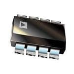
| 描述 | IC POT DGTL 5K 256POS SOT23-8数字电位计 IC IC 8-Bit SPI |
| DevelopmentKit | EVAL-AD5160EBZ |
| 产品分类 | |
| 品牌 | Analog Devices Inc |
| 产品手册 | |
| 产品图片 |
|
| rohs | 符合RoHS无铅 / 符合限制有害物质指令(RoHS)规范要求 |
| 产品系列 | 数字电位计 IC,Analog Devices AD5160BRJZ5-RL7- |
| 数据手册 | |
| 产品型号 | AD5160BRJZ5-RL7 |
| POT数量 | Single |
| 产品目录页面 | |
| 产品种类 | 数字电位计 IC |
| 供应商器件封装 | SOT-23-8 |
| 其它名称 | AD5160BRJZ5-RL7CT |
| 包装 | 剪切带 (CT) |
| 商标 | Analog Devices |
| 存储器类型 | 易失 |
| 安装类型 | 表面贴装 |
| 安装风格 | SMD/SMT |
| 容差 | 15 % |
| 封装 | Reel |
| 封装/外壳 | SOT-23-8 |
| 封装/箱体 | SOT-23-8 |
| 工作温度 | -40°C ~ 125°C |
| 工作电源电压 | 5.5 V |
| 工厂包装数量 | 3000 |
| 弧刷存储器 | Volatile |
| 抽头 | 256 |
| 接口 | 3 线 SPI(芯片选择) |
| 数字接口 | SPI |
| 最大工作温度 | + 125 C |
| 最小工作温度 | - 40 C |
| 标准包装 | 1 |
| 每POT分接头 | 256 |
| 温度系数 | 标准值 45 ppm/°C |
| 电压-电源 | 2.7 V ~ 5.5 V |
| 电源电压-最大 | 5.5 V |
| 电源电压-最小 | 2.7 V |
| 电源电流 | 3 uA |
| 电路数 | 1 |
| 电阻 | 5 kOhms |
| 电阻(Ω) | 5k |
| 系列 | AD5160 |


- 商务部:美国ITC正式对集成电路等产品启动337调查
- 曝三星4nm工艺存在良率问题 高通将骁龙8 Gen1或转产台积电
- 太阳诱电将投资9.5亿元在常州建新厂生产MLCC 预计2023年完工
- 英特尔发布欧洲新工厂建设计划 深化IDM 2.0 战略
- 台积电先进制程称霸业界 有大客户加持明年业绩稳了
- 达到5530亿美元!SIA预计今年全球半导体销售额将创下新高
- 英特尔拟将自动驾驶子公司Mobileye上市 估值或超500亿美元
- 三星加码芯片和SET,合并消费电子和移动部门,撤换高东真等 CEO
- 三星电子宣布重大人事变动 还合并消费电子和移动部门
- 海关总署:前11个月进口集成电路产品价值2.52万亿元 增长14.8%


PDF Datasheet 数据手册内容提取
256-Position SPI-Compatible Digital Potentiometer Data Sheet AD5160 FEATURES FUNCTIONAL BLOCK DIAGRAM 256-position VDD End-to-end resistance: 5 kΩ, 10 kΩ, 50 kΩ, 100 kΩ Compact SOT-23-8 (2.9 mm × 3 mm) package A CS SPI-compatible interface SPI INTERFACE SDI Power-on preset to midscale CLK W Single supply: 2.7 V to 5.5 V Low temperature coefficient: 45 ppm/°C WIPER B Low power, I = 8 μA REGISTER DD Wide operating temperature: –40°C to +125°C Evaluation board available GND Figure 1. APPLICATIONS Mechanical potentiometer replacement in new designs PIN CONFIGURATION Transducer adjustment of pressure, temperature, position, chemical, and optical sensors W 1 8 A RF amplifier biasing VDD 2 AD5160 7 B Gain control and offset adjustment GND 3 TOP VIEW 6 CS CLK 4 (Not to Scale) 5 SDI Figure 2. GENERAL DESCRIPTION The AD5160 provides a compact 2.9 mm × 3 mm packaged The wiper settings are controllable through an SPI-compatible solution for 256-position adjustment applications. These digital interface. The resistance between the wiper and either devices perform the same electronic adjustment function as end point of the fixed resistor varies linearly with respect to the mechanical potentiometers1 or variable resistors but with digital code transferred into the RDAC latch. enhanced resolution, solid-state reliability, and superior low Operating from a 2.7 V to 5.5 V power supply and consuming temperature coefficient performance. less than 5 μA allows for usage in portable battery-operated applications. 1 The terms digital potentiometer, VR, and RDAC are used interchangeably. Rev. C Document Feedback Information furnished by Analog Devices is believed to be accurate and reliable. However, no responsibility is assumed by Analog Devices for its use, nor for any infringements of patents or other One Technology Way, P.O. Box 9106, Norwood, MA 02062-9106, U.S.A. rights of third parties that may result from its use. Specifications subject to change without notice. No license is granted by implication or otherwise under any patent or patent rights of Analog Devices. Tel: 781.329.4700 ©2003–2014 Analog Devices, Inc. All rights reserved. Trademarks and registered trademarks are the property of their respective owners. Technical Support www.analog.com
AD5160 Data Sheet TABLE OF CONTENTS Features .............................................................................................. 1 Typical Performance Characteristics ..............................................8 Applications ....................................................................................... 1 Test Circuits ..................................................................................... 12 Functional Block Diagram .............................................................. 1 SPI Interface .................................................................................... 13 Pin Configuration ............................................................................. 1 Theory of Operation ...................................................................... 14 General Description ......................................................................... 1 Programming the Variable Resistor ......................................... 14 Revision History ............................................................................... 2 Programming the Potentiometer Divider ............................... 15 Specifications ..................................................................................... 3 SPI-Compatible 3-Wire Serial Bus ........................................... 15 Electrical Characteristics—5 kΩ Version .................................. 3 ESD Protection ........................................................................... 15 10 kΩ, 50 kΩ, 100 kΩ Versions .................................................. 4 Power-Up Sequence ................................................................... 15 Timing Characteristics—All Versions ....................................... 5 Layout and Power Supply Bypassing ....................................... 15 Absolute Maximum Ratings ............................................................ 6 Outline Dimensions ....................................................................... 16 ESD Caution .................................................................................. 6 Ordering Guide .......................................................................... 16 Pin Configuration and Function Descriptions ............................. 7 REVISION HISTORY 11/14—Rev. B to Rev. C Changes to Ordering Guide .......................................................... 16 5/09—Rev. A to Rev. B Changes to Ordering Guide .......................................................... 16 1/09—Rev. 0 to Rev. A Deleted Shutdown Supply Current Parameter and Endnote 7, Table 1 ............................................................................ 3 Changes to Resistor Noise Voltage Density Parameter, Table 1 ................................................................................................ 3 Deleted Shutdown Supply Current Parameter and Endnote 7, Table 2 ............................................................................ 4 Changes to Resistor Noise Voltage Density Parameter, Table 2 ................................................................................................ 4 Added Endnote to Table 3 ............................................................... 5 Changes to Table 4 ............................................................................ 6 Changes to the Rheostat Operation Section ............................... 14 Deleted Terminal Voltage Operating Range Section and Figure 41, Renumbered Figures Sequentially ............................. 13 Changes to Figure 40 and Figure 41 ............................................. 15 Changes to Ordering Guide .......................................................... 16 5/03—Revision 0: Initial Version Rev. C | Page 2 of 16
Data Sheet AD5160 SPECIFICATIONS ELECTRICAL CHARACTERISTICS—5 kΩ VERSION V = 5 V ± 10%, or 3 V ± 10%; V = +V ; V = 0 V; –40°C < T < +125°C; unless otherwise noted. DD A DD B A Table 1. Parameter Symbol Conditions Min Typ1 Max Unit DC CHARACTERISTICS Rheostat Mode Resistor Differential Nonlinearity2 R-DNL R , V = no connect −1.5 ±0.1 +1.5 LSB WB A Resistor Integral Nonlinearity2 R-INL R , V = no connect −4 ±0.75 +4 LSB WB A Nominal Resistor Tolerance3 ∆R T = 25°C −20 +20 % AB A Resistance Temperature Coefficient ∆R /∆T V = V , wiper = no connect 45 ppm/°C AB AB DD Wiper Resistance R 50 120 Ω W Potentiometer Divider Mode Specifications apply to all VRs Resolution N 8 Bits Differential Nonlinearity4 DNL −1.5 ±0.1 +1.5 LSB Integral Nonlinearity4 INL −1.5 ±0.6 +1.5 LSB Voltage Divider Temperature Coefficient ∆V /∆T Code = 0x80 15 ppm/°C W Full-Scale Error V Code = 0xFF −6 −2.5 0 LSB WFSE Zero-Scale Error V Code = 0x00 0 +2 +6 LSB WZSE RESISTOR TERMINALS Voltage Range5 V V V GND V V A, B, W DD Capacitance A, Capacitance B6 C f = 1 MHz, measured to GND, code = 0x80 45 pF A,B Capacitance W6 C f = 1 MHz, measured to GND, code = 0x80 60 pF W Common-Mode Leakage I V = V = V /2 1 nA CM A B DD DIGITAL INPUTS Input Logic High V 2.4 V IH Input Logic Low V 0.8 V IL Input Logic High V V = 3 V 2.1 V IH DD Input Logic Low V V = 3 V 0.6 V IL DD Input Current I V = 0 V or 5 V ±1 µA IL IN Input Capacitance6 C 5 pF IL POWER SUPPLIES Power Supply Range V 2.7 5.5 V DD RANGE Supply Current I V = 5 V or V = 0 V 3 8 µA DD IH IL Power Dissipation7 P V = 5 V or V = 0 V, V = 5 V 0.2 mW DISS IH IL DD Power Supply Sensitivity PSS ∆V = +5 V ± 10%, code = midscale ±0.02 ±0.05 %/% DD DYNAMIC CHARACTERISTICS6, 8 Bandwidth –3 dB BW_5K R = 5 kΩ, code = 0x80 1.2 MHz AB Total Harmonic Distortion THD V = 1 V rms, V = 0 V, f = 1 kHz 0.05 % W A B V Settling Time t V = 5 V, V = 0 V, ±1 LSB error band 1 µs W S A B Resistor Noise Voltage Density e R = 2.5 kΩ 6 nV/√Hz N_WB WB 1 Typical specifications represent average readings at +25°C and VDD = 5 V. 2 Resistor position nonlinearity error (R-INL) is the deviation from an ideal value measured between the maximum resistance and the minimum resistance wiper positions. R-DNL measures the relative step change from ideal between successive tap positions. Parts are guaranteed monotonic. 3 VAB = VDD, wiper (VW) = no connect. 4 INL and DNL are measured at VW with the RDAC configured as a potentiometer divider similar to a voltage output digital-to-analog converter (DAC). VA = VDD and VB = 0 V. DNL specification limits of ±1 LSB maximum are guaranteed monotonic operating conditions. 5 Resistor Terminal A, Resistor Terminal B, and Resistor Terminal W have no limitations on polarity with respect to each other. 6 Guaranteed by design and not subject to production test. 7 PDISS is calculated from (IDD × VDD). CMOS logic level inputs result in minimum power dissipation. 8 All dynamic characteristics use VDD = 5 V. Rev. C | Page 3 of 16
AD5160 Data Sheet 10 kΩ, 50 kΩ, 100 kΩ VERSIONS V = 5 V ± 10%, or 3 V ± 10%; V = V ; V = 0 V; −40°C < T < +125°C; unless otherwise noted. DD A DD B A Table 2. Parameter Symbol Conditions Min Typ1 Max Unit DC CHARACTERISTICS Rheostat Mode Resistor Differential Nonlinearity2 R-DNL R , V = no connect −1 ±0.1 +1 LSB WB A Resistor Integral Nonlinearity2 R-INL R , V = no connect −2 ±0.25 +2 LSB WB A Nominal Resistor Tolerance3 ∆R T = 25°C −15 +15 % AB A Resistance Temperature Coefficient ∆R /∆T V = V , 45 ppm/°C AB AB DD Wiper = no connect Wiper Resistance R V = 5 V 50 120 Ω W DD Potentiometer Divider Mode Specifications apply to all VRs Resolution N 8 Bits Differential Nonlinearity4 DNL −1 ±0.1 +1 LSB Integral Nonlinearity4 INL −1 ±0.3 +1 LSB Voltage Divider Temperature ∆V /∆T Code = 0x80 15 ppm/°C W Coefficient Full-Scale Error V Code = 0xFF −3 −1 0 LSB WFSE Zero-Scale Error V Code = 0x00 0 1 3 LSB WZSE RESISTOR TERMINALS Voltage Range5 V GND V V A,B,W DD Capacitance A, Capacitance B6 C f = 1 MHz, measured to GND, code = 45 pF A,B 0x80 Capacitance W6 C f = 1 MHz, measured to GND, code = 60 pF W 0x80 Common-Mode Leakage I V = V = V /2 1 nA CM A B DD DIGITAL INPUTS Input Logic High V 2.4 V IH Input Logic Low V 0.8 V IL Input Logic High V V = 3 V 2.1 V IH DD Input Logic Low V V = 3 V 0.6 V IL DD Input Current I V = 0 V or 5 V ±1 µA IL IN Input Capacitance6 C 5 pF IL POWER SUPPLIES Power Supply Range V 2.7 5.5 V DD RANGE Supply Current I V = 5 V or V = 0 V 3 8 µA DD IH IL Power Dissipation7 P V = 5 V or V = 0 V, V = 5 V 0.2 mW DISS IH IL DD Power Supply Sensitivity PSS ∆V = +5 V ± 10%, code = midscale ±0.02 ±0.05 %/% DD DYNAMIC CHARACTERISTICS6, 8 Bandwidth –3 dB BW R = 10 kΩ/50 kΩ/100 kΩ, Code = 0x80 600/100/40 kHz AB Total Harmonic Distortion THD V = 1 V rms, V = 0 V, f = 1 kHz, R = 0.05 % W A B AB 10 kΩ V Settling Time (10 kΩ/50 kΩ/100 kΩ) t V = 5 V, V = 0 V, 2 µs W S A B ±1 LSB error band Resistor Noise Voltage Density e R = 5 kΩ 9 nV/√Hz N_WB WB 1 Typical specifications represent average readings at +25°C and VDD = 5 V. 2 Resistor position nonlinearity error (R-INL) is the deviation from an ideal value measured between the maximum resistance and the minimum resistance wiper positions. R-DNL measures the relative step change from ideal between successive tap positions. Parts are guaranteed monotonic. 3 VAB = VDD, wiper (VW) = no connect. 4 INL and DNL are measured at VW with the RDAC configured as a potentiometer divider similar to a voltage output digital-to-analog converter (DAC). VA = VDD and VB = 0 V. DNL specification limits of ±1 LSB maximum are guaranteed monotonic operating conditions. 5 Resistor Terminal A, Resistor Terminal B, and Resistor Terminal W have no limitations on polarity with respect to each other. 6 Guaranteed by design and not subject to production test. 7 PDISS is calculated from (IDD × VDD). CMOS logic level inputs result in minimum power dissipation. 8 All dynamic characteristics use VDD = 5 V. Rev. C | Page 4 of 16
Data Sheet AD5160 TIMING CHARACTERISTICS—ALL VERSIONS V = +5V ± 10%, or +3V ± 10%; V = V ; V = 0 V; –40°C < T < +125°C; unless otherwise noted. DD A DD B A Table 3. Parameter Symbol Conditions Min Typ1 Max Unit SPI INTERFACE TIMING CHARACTERISTICS1, 2 Specifications apply to all parts Clock Frequency f 25 MHz CLK Input Clock Pulse Width t , t Clock level high or low 20 ns CH CL Data Setup Time t 5 ns DS Data Hold Time t 5 ns DH CS Setup Time tCSS 15 ns CS High Pulse Width tCSW 40 ns CLK Fall to CS Fall Hold Time tCSH0 0 ns CLK Fall to CS Rise Hold Time tCSH1 0 ns 1 See the timing diagram, Figure 38, for location of measured values. All input control voltages are specified with tR = tF = 2 ns (10% to 90% of 3 V) and timed from a voltage level of 1.5 V. 2 Guaranteed by design and not subject to production test. Rev. C | Page 5 of 16
AD5160 Data Sheet ABSOLUTE MAXIMUM RATINGS T = +25°C, unless otherwise noted. A Stresses at or above those listed under Absolute Maximum Table 4. Ratings may cause permanent damage to the product. This is a Parameter Rating stress rating only; functional operation of the product at these V to GND −0.3 V to +7 V DD or any other conditions above those indicated in the operational V , V , V to GND V A B W DD section of this specification is not implied. Operation beyond Maximum Current I 1 MAX the maximum operating conditions for extended periods may I , I Pulsed ±20 mA WB WA affect product reliability. I , I Continuous WB WA 5 kΩ, 10 kΩ 4.7 mA ESD CAUTION 50 kΩ 0.95 mA 100 kΩ 0.48 mA Digital Inputs and Output Voltage to GND 0 V to +7 V Temperature Operating Temperature Range −40°C to +125°C Maximum Junction Temperature (T ) 150°C JMAX Storage Temperature −65°C to +150°C Thermal Resistance (SOT-23 Package)2 θ Thermal Impedance 206ºC/W JA θ Thermal Impedance 91°C/W JC Reflow Soldering (Pb-Free) Peak Temperature 260°C Time at Peak Temperature 10 sec to 40 sec 1 Maximum terminal current is bounded by the maximum current handling of the switches, maximum power dissipation of the package, and applied voltage across any two of the A, B, and W terminals at a given resistance. 2 Package power dissipation = (TJMAX − TA)/θJA. Rev. C | Page 6 of 16
Data Sheet AD5160 PIN CONFIGURATION AND FUNCTION DESCRIPTIONS W 1 8 A VDD 2 AD5160 7 B GND 3 TOP VIEW 6 CS CLK 4 (Not to Scale) 5 SDI Figure 3. Pin Configuration Table 5. Pin Function Descriptions Pin Mnemonic Description 1 W W Terminal. 2 V Positive Power Supply. DD 3 GND Digital Ground. 4 CLK Serial Clock Input. Positive edge triggered. 5 SDI Serial Data Input. 6 CS Chip Select Input, Active Low. When CS returns high, data loads into the DAC register. 7 B B Terminal. 8 A A Terminal. Rev. C | Page 7 of 16
AD5160 Data Sheet TYPICAL PERFORMANCE CHARACTERISTICS 1.0 1.0 0.8 5V 0.8 –40°C 3V +25°C B) 0.6 B) 0.6 ++18255°°CC NL (LS 0.4 NL (LS 0.4 MODE I 00.2 MODE D 00.2 RHEOSTAT ––00..42 TIOMETER ––00..42 –0.6 EN–0.6 T O –0.8 P–0.8 –1.0 –1.0 0 32 64 96 128 160 192 224 256 0 32 64 96 128 160 192 224 256 CODE (Decimal) CODE (Decimal) Figure 4. R-INL vs. Code vs. Supply Voltages Figure 7. DNL vs. Code, VDD = 5 V 1.0 1.0 0.8 0.8 5V 5V SB) 0.6 3V SB) 0.6 3V L L NL ( 0.4 NL ( 0.4 RHEOSTAT MODE D––000..420.2 NTIOMETER MODE I––000..420.2 E T –0.6 O–0.6 P –0.8 –0.8 –1.0 –1.0 0 32 64 96 128 160 192 224 256 0 32 64 96 128 160 192 224 256 CODE (Decimal) CODE (Decimal) Figure 5. R-DNL vs. Code vs. Supply Voltages Figure 8. INL vs. Code vs. Supply Voltages 1.0 1.0 0.8 _40°C 0.8 5V B) 0.6 +++1282555°°°CCC LSB) 0.6 3V NL (LS 0.4 E DNL( 0.4 MODE I 00.2 R MOD 0.20 R TE TE–0.2 ME–0.2 NTIOME–0.4 TENTIO–0.4 E–0.6 O–0.6 OT P P–0.8 –0.8 –1.0 –1.0 0 32 64 96 128 160 192 224 256 0 32 64 96 128 160 192 224 256 CODE (Decimal) CODE (Decimal) Figure 6. INL vs. Code, VDD = 5 V Figure 9. DNL vs. Code vs. Supply Voltages Rev. C | Page 8 of 16
Data Sheet AD5160 1.0 2.5 –40°C 0.8 +25°C NL (LSB) 00..46 ++18255°°CC µOR (A)2.0 DE I 0.2 ERR1.5 VDD = 5.5V TAT MO 0 SCALE VDD = 2.7V RHEOS––00..42 E, ZERO-1.0 S –0.6 Z0.5 –0.8 –1.0 0 0 32 64 96 128 160 192 224 256 ––4400 00 4400 8800 112200 CODE (Decimal) TEMPERATURE (°C) Figure 10. R-INL vs. Code, VDD = 5 V Figure 13. Zero-Scale Error vs. Temperature 1.0 10 _40°C 0.8 +25°C B) +85°C S 0.6 +125°C DNL (L 0.4 µT (A) T MODE 00.2 CURREN 1 VDD = 5.5V OSTA–0.2 PPLY E U RH–0.4 SD D –0.6 I VDD = 2.7V –0.8 –1.0 0.1 0 32 64 96 128 160 192 224 256 –40 0 40 80 120 CODE (Decimal) TEMPERATURE (°C) Figure 11. R-DNL vs. Code, VDD = 5 V Figure 14. Supply Current vs. Temperature 2.5 70 60 SB)2.0 A) L n R ( T ( 50 O N R E R1.5 R ALE E VDD = 2.7V N CUR 40 C W L-S1.0 DO 30 E, FUL VDD = 5.5V SHUT 20 VDD = 5V FS0.5 IA 10 0 0 ––4400 00 4400 8800 112200 –40 0 40 80 120 TEMPERATURE (°C) TEMPERATURE (°C) Figure 12. Full-Scale Error vs. Temperature Figure 15. Shutdown Current vs. Temperature Rev. C | Page 9 of 16
AD5160 Data Sheet 200 REF LEVEL /DIV MARKER 510 634.725Hz 0.000dB 6.000dB MAG (A/R) –9.049dB 0 C) m/° 150 –6 0x80 p O (p –12 0x40 C MP 100 –18 0x20 E E T –24 0x10 D MO 50 –30 0x08 T 0x04 STA –36 0x02 EO 0 –42 0x01 H R –48 –50 –54 0 32 64 96 128 160 192 224 256 CODE (Decimal) –60 1k 10k 100k 1M START 1 000.000Hz STOP 1 000 000.000Hz Figure 16. Rheostat Mode Tempco ∆RWB/∆T vs. Code Figure 19. Gain vs. Frequency vs. Code, RAB = 10 kΩ 160 REF LEVEL /DIV MARKER 100 885.289Hz 0.000dB 6.000dB MAG (A/R) –9.014dB m/°C)140 0 (pp120 –6 0x80 CO –12 0x40 P100 M ODE TE 80 ––1284 00xx2100 M 60 R –30 0x08 E ET 40 0x04 M –36 O NTI 20 –42 0x02 OTE 0 –48 0x01 P –20 –54 0 32 64 96 128 160 192 224 256 CODE (Decimal) –60 1k 10k 100k 1M START 1 000.000Hz STOP 1 000 000.000Hz Figure 17. Potentiometer Mode Tempco ∆VWB/∆T vs. Code Figure 20. Gain vs. Frequency vs. Code, RAB = 50 kΩ REF LEVEL /DIV MARKER 1 000 000.000Hz REF LEVEL /DIV MARKER 54 089.173Hz 0.000dB 6.000dB MAG (A/R) –8.918dB 0.000dB 6.000dB MAG (A/R) –9.052dB 0 0 –6 0x80 –6 0x80 –12 0x40 –12 0x40 –18 0x20 –18 0x20 –24 0x10 –24 0x10 0x08 –30 0x04 –30 0x08 –36 00xx0021 –36 0x04 –42 –42 0x02 –48 –48 0x01 –54 –54 –60 –60 1k 10k 100k 1M 1k 10k 100k 1M START 1 000.000Hz STOP 1 000 000.000Hz START 1 000.000Hz STOP 1 000 000.000Hz Figure 18. Gain vs. Frequency vs. Code, RAB = 5 kΩ Figure 21. Gain vs. Frequency vs. Code, RAB = 100 kΩ Rev. C | Page 10 of 16
Data Sheet AD5160 REF LEVEL /DIV –5.000dB 0.500dB –5.5 –6.0 5k– 1.026 MHz 10k– 511 MHz –6.5 50k– 101 MHz 100k– 54 MHz –7.0 1 VW –7.5 –8.0 CLK –8.5 R = 50k R = 5k 2 –9.0 –9.5 R = 100k R = 10k Ch 1 200mV BWCh 2 5.00 V BWM 100ns A CH2 3.00 V –10.0 –10.5 10k 100k 1M 10M START 1 000.000Hz STOP 1 000 000.000Hz Figure 22. –3 dB Bandwidth @ Code = 0x80 Figure 25. Digital Feedthrough 60 CODE = 0x80, VA= VDD, VB = 0V VA = 5V VB = 0V 40 B) RR (d PSRR @ VDD = 3V DC± 10% p-p AC 1 VW S P 20 CS 2 PSRR @ VDD = 5V DC± 10% p-p AC Ch 1 100mV BWCh 2 5.00 V BWM 200ns A CH1 152mV 0 100 1k 10k 100k 1M FREQUENCY (Hz) Figure 23. PSRR vs. Frequency Figure 26. Midscale Glitch, Code 0x80 to Code 0x7F 900 VDD= 5V 800 VA = 5V VB = 0V 700 600 500 1 VW A) (D 400 CODE = 0x55 D I CS 300 CODE = 0xFF 2 200 100 Ch 1 5.00V BWCh 2 5.00 V BWM 200ns A CH1 3.00 V 0 10k 100k 1M 10M FREQUENCY (Hz) Figure 24. IDD vs. Frequency Figure 27. Large Signal Settling Time, Code 0xFF to Code 0x00 Rev. C | Page 11 of 16
AD5160 Data Sheet TEST CIRCUITS Figure 28 to Figure 36 illustrate the test circuits that define the test conditions used in the product specification tables. 5V DUT 1VL+S=B V =D DV+/2N OP279 VOUT V+ A W VIN W B OFFSET VMS GND A DUT B OFFSET BIAS Figure 28. Test Circuit for Potentiometer Divider Nonlinearity Error (INL, DNL) Figure 33. Test Circuit for Noninverting Gain NO CONNECT A DUT +15V A IW VIN DUT W W OFFSET AD8610 VOUT B GND B VMS 2.5V –15V Figure 29. Test Circuit for Resistor Position Nonlinearity Error Figure 34. Test Circuit for Gain vs. Frequency (Rheostat Operation; R-INL, R-DNL) 0.1V DUT DUT RSW= ISW VMS2 A W VW IW= VDD/RNOMINAL W CODE = 0x00 B B ISW 0.1V VMS1 RW= [VMS1– VMS2]/IW VSS TO VDD Figure 30. Test Circuit for Wiper Resistance Figure 35. Test Circuit for Incremental On Resistance VA NC V+ VDD A W PPV+SS SR= RV(% D(dD/%B))1 ==0 %2∆0V LMOS%G( ∆∆ VV MD DS ) VDD DUT AW ICM B ∆VDD% VSS GND B VCM VMS NC NC = NO CONNECT Figure 31. Test Circuit for Power Supply Sensitivity (PSS, PSSR) Figure 36. Test Circuit for Common-Mode Leakage Current A DUT B 5V VIN W OFFSET OP279 VOUT GND OFFSET BIAS Figure 32. Test Circuit for Inverting Gain Rev. C | Page 12 of 16
Data Sheet AD5160 SPI INTERFACE Table 6. Serial Data-Word Format 1 SDI D7 D6 D5 D4 D3 D2 D1 D0 0 B7 B6 B5 B4 B3 B2 B1 B0 1 CLK D7 D6 D5 D4 D3 D2 D1 D0 0 MSB LSB CS 1 RDAC REGISTER LOAD 0 27 20 1 VOUT 0 Figure 37. SPI Interface Timing Diagram (VA = 5 V, VB = 0 V, VW = VOUT) 1 SDI (DATA IN) Dx Dx 0 1 tCH tDS tCH tCS1 CLK 0 tCSHO tCL tCSH1 tCSS 1 CS tCSW 0 tS VDD VOUT ±1LSB 0 Figure 38. SPI Interface Detailed Timing Diagram (VA = 5 V, VB = 0 V, VW = VOUT) Rev. C | Page 13 of 16
AD5160 Data Sheet THEORY OF OPERATION The AD5160 is a 256-position digitally controlled variable The general equation determining the digitally programmed resistor (VR) device. output resistance between W and B is An internal power-on preset places the wiper at midscale D R (D) R R (1) during power-on, which simplifies the fault condition recovery WB 256 AB W at power-up. where: PROGRAMMING THE VARIABLE RESISTOR D is the decimal equivalent of the binary code loaded in the Rheostat Operation 8-bit RDAC register. R is the end-to-end resistance. The nominal resistance of the RDAC between Terminal A and AB R is the wiper resistance contributed by the on resistance of Terminal B is available in 5 kΩ, 10 kΩ, 50 kΩ, and 100 kΩ. The W the internal switch. final two or three digits of the model number as listed in the Ordering Guide section determine the nominal resistance value, In summary, if RAB = 10 kΩ and the A terminal is open for example, in model AD5160BRJZ10, the 10 represents 10 kΩ; circuited, the following output resistance RWB is set for the and in AD5160BRJZ50, the 50 represents 50 kΩ. indicated RDAC latch codes. The nominal resistance (RAB) of the VR has 256 contact points Table 7. Codes and Corresponding RWB Resistance accessed by the wiper terminal, plus the B terminal contact. The D (Dec.) R (Ω) Output State WB 8-bit data in the RDAC latch is decoded to select one of the 256 255 9961 Full Scale (R − 1 LSB + R ) AB W possible settings. 128 5060 Midscale Assuming a 10 kΩ part is used, the first connection of the wiper 1 99 1 LSB starts at the B terminal for Data 0x00. Because there is a 60 Ω 0 60 Zero Scale (Wiper Contact Resistance) wiper contact resistance, such connection yields a minimum of Note that in the zero-scale condition, a finite wiper resistance of 60 Ω resistance between Terminal W and Terminal B. 60 Ω is present. Take care to limit the current flow between W The second connection is the first tap point, which corresponds and B in this state to a maximum pulse current of no more than to 99 Ω (R = R /256 + R = 39 Ω + 60 Ω) for Data 0x01. 20 mA. Otherwise, degradation or possible destruction of the WB AB W internal switch contact can occur. The third connection is the next tap point, representing 138 Ω (2 × 39 Ω + 60 Ω) for Data 0x02, and so on. Each LSB data Similar to the mechanical potentiometer, the resistance of the value increase moves the wiper up the resistor ladder until the RDAC between the Wiper W and Terminal A also produces a last tap point is reached at 9961 Ω (R − 1 LSB + R ). Figure 39 digitally controlled complementary resistance (R ). When AB W WA shows a simplified diagram of the equivalent RDAC circuit these terminals are used, the B terminal can be opened. Setting where the last resistor string is not accessed; therefore, there is the resistance value for R starts at a maximum value of WA 1 LSB less of the nominal resistance at full scale in addition to resistance and decreases as the data loaded in the latch increases the wiper resistance. in value. The general equation for this operation is A 256D R (D) R R (2) WA AB W 256 RS For R = 10 kΩ and the B terminal is open circuited, the AB D7 DD65 RS following output resistance RWA is set for the indicated RDAC D4 latch codes. D3 D2 RS D1 Table 8. Codes and Corresponding R Resistance D0 W WA D (Dec.) R (Ω) Output State WA 255 99 Full Scale RDAC 128 5060 Midscale LATCH AND RS B 1 9961 1 LSB DECODER 0 10,060 Zero Scale Typical device-to-device matching is process lot dependent and Figure 39. Equivalent RDAC Circuit may vary by up to ±30%. Because the resistance element is processed in thin film technology, the change in R with AB temperature has a very low 45 ppm/°C temperature coefficient. Rev. C | Page 14 of 16
Data Sheet AD5160 PROGRAMMING THE POTENTIOMETER DIVIDER ESD PROTECTION Voltage Output Operation All digital inputs are protected with a series input resistor and The digital potentiometer easily generates a voltage divider at parallel Zener ESD structures are shown in Figure 40 and wiper-to-B and wiper-to-A proportional to the input voltage at Figure 41. This applies to SDI, CLK, and CS, which are the A-to-B. Unlike the polarity of V to GND, which must be digital input pins. DD positive, voltage across A to B, W to A, and W to B can be at 340Ω either polarity. LOGIC If ignoring the effect of the wiper resistance for approximation, GND connecting the A terminal to 5 V and the B terminal to ground Figure 40. ESD Protection of Digital Pins produces an output voltage at the wiper-to-B starting at 0 V up A,B,W to 1 LSB less than 5 V. Each LSB of voltage is equal to the voltage applied across Terminal A and Terminal B divided by GND the 256 positions of the potentiometer divider. The general Figure 41. ESD Protection of Resistor Terminals equation defining the output voltage at V with respect to W POWER-UP SEQUENCE ground for any valid input voltage applied to Terminal A and Terminal B is Because the ESD protection diodes limit the voltage compliance D 256D at the A, B, and W terminals, it is important to power VDD/GND V (D) V V (3) W A B before applying any voltage to the A, B, and W terminals; 256 256 otherwise, the diode forward biases such that V is powered DD For a more accurate calculation, which includes the effect of unintentionally and may affect the rest of the user’s circuit. The wiper resistance, V can be found as W ideal power-up sequence is in the following order: GND, V , DD R (D) R (D) digital inputs, and then V . The relative order of powering V (D) WB V WA V (4) A/B/W W 256 A 256 B VA, VB, VW, and the digital inputs is not important as long as they are powered after V /GND. Operation of the digital potentiometer in the divider mode DD results in a more accurate operation over temperature. Unlike LAYOUT AND POWER SUPPLY BYPASSING the rheostat mode, the output voltage is dependent mainly on It is a good practice to employ compact, minimum lead length the ratio of the internal resistors (R and R ) and not the WA WB layout design. Keep the leads to the inputs as direct as possible absolute values. Therefore, the temperature drift reduces to with a minimum conductor length. Ground paths should have 15 ppm/°C. low resistance and low inductance. SPI-COMPATIBLE 3-WIRE SERIAL BUS Similarly, it is also a good practice to bypass the power supplies The AD5160 contains a 3-wire SPI-compatible digital interface with quality capacitors for optimum stability. Bypass supply (SDI, CS, and CLK). The 8-bit serial word must be loaded MSB leads to the device with disc or chip ceramic capacitors of first. The format of the word is shown in Table 6. 0.01 μF to 0.1 μF. To minimize any transient disturbance and low frequency ripple, apply low ESR 1 μF to 10 μF tantalum or The positive-edge sensitive CLK input requires clean transitions electrolytic capacitors at the supplies (see Figure 42). To to avoid clocking incorrect data into the serial input register. minimize the ground bounce, join the digital ground remotely Standard logic families work well. If mechanical switches are to the analog ground at a single point. used for product evaluation, they should be debounced by a flip-flop or other suitable means. When CS is low, the clock loads data into the serial register on each positive clock edge (see Figure 37). VDD VDD The data setup and data hold times in the specification table C3 + C1 10F 0.1F determine the valid timing requirements. The AD5160 uses an AD5160 8-bit serial input data register word that is transferred to the internal RDAC register when the CS line returns to logic high. GND Extra MSB bits are ignored. Figure 42. Power Supply Bypassing Rev. C | Page 15 of 16
AD5160 Data Sheet OUTLINE DIMENSIONS 3.00 2.90 2.80 1.70 8 7 6 5 3.00 1.60 2.80 1.50 2.60 1 2 3 4 PIN1 INDICATOR 0.65BSC 1.95 BSC 1.30 1.15 0.90 1.45MAX 0.22MAX 0.95MIN 0.08MIN 0.60 0.15MAX 8° 0.45 0.05MIN 0.38MAX SPLEAATNIENG 4° B0S.6C0 0.30 0.22MIN 0° COMPLIANTTOJEDECSTANDARDSMO-178-BA 12-16-2008-A Figure 43. 8-Lead Small Outline Transistor Package [SOT-23] (RJ-8) Dimensions shown in millimeters ORDERING GUIDE Model1, 2, 3 R (Ω) Temperature Package Description Package Option Branding AB AD5160BRJZ5-R2 5 k −40°C to +125°C 8-Lead SOT-23 RJ-8 D6Q AD5160BRJZ5-RL7 5 k −40°C to +125°C 8-Lead SOT-23 RJ-8 D6Q AD5160BRJZ10-R2 10 k −40°C to +125°C 8-Lead SOT-23 RJ-8 D09 AD5160BRJZ10-RL7 10 k −40°C to +125°C 8-Lead SOT-23 RJ-8 D09 AD5160BRJZ50-R2 50 k −40°C to +125°C 8-Lead SOT-23 RJ-8 D8J AD5160BRJZ50-RL7 50 k −40°C to +125°C 8-Lead SOT-23 RJ-8 D8J AD5160BRJZ100-R2 100 k −40°C to +125°C 8-Lead SOT-23 RJ-8 D0B AD5160BRJZ100-RL7 100 k −40°C to +125°C 8-Lead SOT-23 RJ-8 D0B EVAL-AD5160DBZ Evaluation Board 1 The AD5160 contains 2532 transistors. Die size: 30.7 mil × 76.8 mil = 2358 sq. mil. 2 Z = RoHS Compliant Part. 3 The EVAL-AD5160DBZ board is shipped with the 10 kΩ RAB resistor option; however, the board is compatible with all available resistor value options. ©2003–2014 Analog Devices, Inc. All rights reserved. Trademarks and registered trademarks are the property of their respective owners. D03434-0-11/14(C) Rev. C | Page 16 of 16
Mouser Electronics Authorized Distributor Click to View Pricing, Inventory, Delivery & Lifecycle Information: A nalog Devices Inc.: AD5160BRJZ100-R2 AD5160BRJZ100-RL7 AD5160BRJZ10-R2 AD5160BRJZ10-RL7 AD5160BRJZ50-RL7 AD5160BRJZ5-R2 AD5160BRJZ5-RL7 EVAL-AD5160DBZ