ICGOO在线商城 > 集成电路(IC) > 时钟/计时 - 可编程计时器和振荡器 > AD2S99BP
 Datasheet下载
- 型号: AD2S99BP
- 制造商: Analog
- 库位|库存: xxxx|xxxx
- 要求:
| 数量阶梯 | 香港交货 | 国内含税 |
| +xxxx | $xxxx | ¥xxxx |
查看当月历史价格
查看今年历史价格
AD2S99BP产品简介:
ICGOO电子元器件商城为您提供AD2S99BP由Analog设计生产,在icgoo商城现货销售,并且可以通过原厂、代理商等渠道进行代购。 AD2S99BP价格参考。AnalogAD2S99BP封装/规格:时钟/计时 - 可编程计时器和振荡器, Oscillator, Sinusoidal IC 2kHz ~ 20kHz 20-PLCC (9x9)。您可以下载AD2S99BP参考资料、Datasheet数据手册功能说明书,资料中有AD2S99BP 详细功能的应用电路图电压和使用方法及教程。
AD2S99BP是由Analog Devices Inc.(ADI公司)生产的一款时钟/计时 - 可编程计时器和振荡器,其主要应用场景包括:

1. 工业自动化与控制:
   AD2S99BP可用于工业设备中的精密定时控制,例如机器人运动控制、电机驱动器以及数据采集系统。它能够提供稳定的时钟信号,确保系统同步性和精度。

2. 通信设备:
   在通信领域中,该器件适用于基站、路由器或交换机等需要精确时钟源的设备。通过可编程功能,可以灵活调整输出频率以满足不同协议需求。

3. 仪器仪表:
   用于测试测量仪器(如示波器、频谱分析仪)中作为参考时钟源,保证信号采样率的一致性及准确性。

4. 消费电子:
   在一些高端家用电器或多媒体播放器里也可能用到此芯片,为音频/视频处理单元提供高质量的时钟支持。

5. 汽车电子:
   随着汽车智能化发展,AD2S99BP还可以应用于车载信息系统、导航设备以及娱乐系统当中,为其提供可靠的时间基准。

6. 航空航天与国防:
   对于要求极高稳定性和可靠性的应用环境,比如卫星通信、雷达系统等领域,这款产品同样表现出色。

总之,AD2S99BP凭借其卓越性能和灵活性,在众多需要精准计时与同步控制的应用场合发挥着重要作用。
| 参数 | 数值 |
| 产品目录 | 集成电路 (IC)无源元件 |
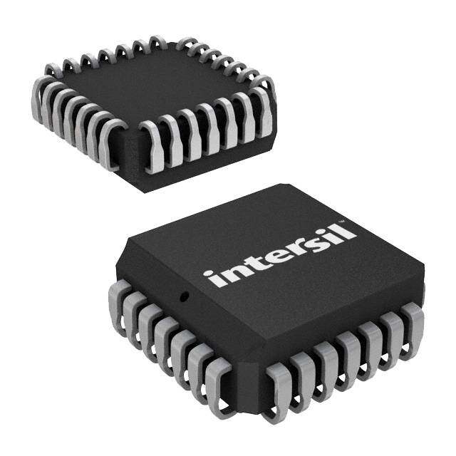
| 描述 | IC OSC SINUSOIDAL PROG 20-PLCC可编程振荡器 IC PROGRAMMABLE OSCILLATOR |
| 产品分类 | |
| 品牌 | Analog Devices Inc |
| 产品手册 | |
| 产品图片 |
|
| rohs | 否无铅 / 不符合限制有害物质指令(RoHS)规范要求 |
| 产品系列 | 振荡器,可编程振荡器,Analog Devices AD2S99BP- |
| 数据手册 | |
| 产品型号 | AD2S99BP |
| 产品 | Programmable |
| 产品种类 | |
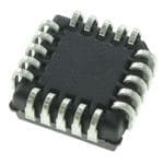
| 供应商器件封装 | 20-PLCC(9x9) |
| 包装 | 管件 |
| 商标 | Analog Devices |
| 安装类型 | 表面贴装 |
| 安装风格 | SMD/SMT |
| 封装 | Tube |
| 封装/外壳 | 20-LCC(J 形引线) |
| 封装/箱体 | PLCC-20 |
| 尺寸 | 9.04 mm W x 9.04 mm L x 4.57 mm H |
| 工作温度 | -40°C ~ 85°C |
| 工厂包装数量 | 49 |
| 最大工作温度 | + 85 C |
| 最小工作温度 | - 40 C |
| 标准包装 | 1 |
| 电压-电源 | ±4.75 V ~ 5.25 V |
| 电流-电源 | 8mA |
| 电源电压 | 4.75 V to 5.25 V |
| 电源电压-最大 | 5.25 V |
| 电源电压-最小 | 4.75 V |
| 端接类型 | SMD/SMT |
| 类型 | 振荡器 - 正弦 |
| 系列 | AD2S99 |
| 计数 | - |
| 负载电容 | 1000 pF |
| 输出格式 | Sinewave |
| 频率 | 2kHz ~ 20kHz |


- 商务部:美国ITC正式对集成电路等产品启动337调查
- 曝三星4nm工艺存在良率问题 高通将骁龙8 Gen1或转产台积电
- 太阳诱电将投资9.5亿元在常州建新厂生产MLCC 预计2023年完工
- 英特尔发布欧洲新工厂建设计划 深化IDM 2.0 战略
- 台积电先进制程称霸业界 有大客户加持明年业绩稳了
- 达到5530亿美元!SIA预计今年全球半导体销售额将创下新高
- 英特尔拟将自动驾驶子公司Mobileye上市 估值或超500亿美元
- 三星加码芯片和SET,合并消费电子和移动部门,撤换高东真等 CEO
- 三星电子宣布重大人事变动 还合并消费电子和移动部门
- 海关总署:前11个月进口集成电路产品价值2.52万亿元 增长14.8%


PDF Datasheet 数据手册内容提取
a Programmable Oscillator AD2S99 FEATURES FUNCTIONAL BLOCK DIAGRAM Programmable Sinusoidal Oscillator Synthesized Synchronous Reference Output ProgrammableOutputFrequencyRange: 2kHz–20 kHz PUSH/ EXC “Loss-of-Signal” Indicator PULL TTORANSDUCER O/P STAGE EXC 20-Pin PLCC Package Low Cost FBIAS APPLICATIONS SEL1 FRSEEQLUEECNTCY GSEINNEE RWAATVOER Excitation Source for: SEL2 Resolvers SYNREF SYNCHRONOUS Synchros PHASE REFERENCE DETECT LVDTs AD2S99 LOGIC LOS RVDTs Pressure Transducers SIN COS Load Cells AC Bridges FROM TRANSDUCER GENERAL DESCRIPTION PRODUCT HIGHLIGHTS The AD2S99 programmable sinusoidal oscillator provides sine Dynamic Phase Compensation wave excitation for resolvers and a wide variety of ac transduc- The AD2S99 dynamically compensates for any phase variation ers. The AD2S99 also provides a synchronous reference output in a transducer by phase locking its synchronous reference out- signal (3 V p-p square wave) that is phase locked to its SIN and put to the transducer’s secondary windings. COS inputs. In an application, the SIN and COS inputs are Programmable Excitation Frequency connected to the transducer’s secondary windings. The excitation frequency is easily programmed to 2 kHz, 5 kHz, The synchronous reference output compensates for temperature 10 kHz, or 20 kHz by using the frequency select pins. Interme- and cabling dependent phase shifts and eliminates the need for diate frequencies are available by adding an external resistor. external preset phase compensation circuits. The synchronous Signal Loss Detection reference output can be used as a zero crossing reference for The AD2S99 has the ability to detect if both the transducer sec- resolver-to-digital converters such as Analog Devices’ AD2S80A, ondary winding connections become disconnected from its SIN AD2S82A, AD2S83 and AD2S90. and COS inputs. The “LOS” output pin pulls high when a sig- The AD2S99 is packaged in a 20-pin PLCC and operates over nal loss is detected. –40(cid:176) C to +85(cid:176) C. Integration The AD2S99 integrates the transducer excitation, synchronous reference, and loss of signal detection functions into a small, cost effective package. REV.B Information furnished by Analog Devices is believed to be accurate and © Analog Devices, Inc., 1995 reliable. However, no responsibility is assumed by Analog Devices for its use, nor for any infringements of patents or other rights of third parties which may result from its use. No license is granted by implication or One Technology Way, P.O. Box 9106, Norwood. MA 02062-9106, U.S.A. otherwise under any patent or patent rights of Analog Devices. Tel: 617/329-4700 Fax: 617/326-8703
AD2S99–SPECIFICATIONS (V = (cid:54)4.75V to (cid:54)5.25 V @ –40(cid:56)C to +85(cid:56)C unless otherwise noted) S Parameter Min Typ Max Units Test Conditions FREQUENCY OUTPUT RANGE SEL1 SEL2 2 kHz 2000 Hz V V SS SS 5 kHz 5000 Hz V GND SS 10 kHz 10000 Hz GND V SS 20 kHz 20000 Hz GND GND ACCURACY Frequency – 10 % AP Grade @ +25(cid:176) C – 20 % AP Grade –40(cid:176) C to +85(cid:176) C – 5 % BP Grade @ +25(cid:176) C – 10 % BP Grade –40(cid:176) C to +85(cid:176) C Amplitude – 3 – 10 % AP Grade @ +25(cid:176) C – 20 % AP Grade –40(cid:176) C to +85(cid:176) C – 3 – 5 % BP Grade @ +25(cid:176) C – 10 % BP Grade –40(cid:176) C to +85(cid:176) C Power Supply Rejection Ratio 0.002 V p-p/V Output Variation as Function of Change in Power Supply Voltage ANALOG OUTPUTS Amplitude EXC, EXC 2 V rms EXC to GND, EXC to GND SYNREF – 3 V p-p Square Wave SYNREF OFFSET – 200 mV Current Drive Capability EXC, EXC V = – 5 V 8 mA rms R = 500 W EXC to EXC S LOAD C = 1000 pF LOAD Capacitive Drive 1000 pF Total Harmonic Distortion EXC, EXC –25 dB ANALOG INPUTS SIN, COS Amplitude 1.8 2.0 2.2 V rms Phase Lock Range –45 +45 Degrees Additional Phase Delay – 10 Degrees AP Grade – 10 Degrees BP Grade FREQUENCY SELECT INPUTS SEL1, SEL21 V AGND V dc SS LOS OUTPUT Output Low Voltage 0.7 V dc I = 400 m A OL Output High Voltage V V dc 50 kW Pull Up to V (Open DD DD Drain Output) SIN, COS LOS Threshold 0.5 0.6 0.8 V rms POWER SUPPLIES V +4.75 +5.25 V dc DD V –4.75 –5.25 V dc SS Quiescent Current I , I – 8 – 15 mA No Load DD SS TEMPERATURE RANGE Operating –40 +85 (cid:176) C Storage –65 +150 (cid:176) C NOTES 1Frequency select pins SEL1 and SEL2 must be connected to appropriate voltage levels before power is applied. Specifications subject to change without notice. –2– REV. B
AD2S99 ABSOLUTE MAXIMUM RATINGS* PIN DESIGNATIONS V . . . . . . . . . . . . . . . . . . . . . . . . . . . . . . . . . . . . . . . . . +7 V DD Pin V . . . . . . . . . . . . . . . . . . . . . . . . . . . . . . . . . . . . . . . . . . –7 V SS Operating Temperature . . . . . . . . . . . . . . . . . .–40(cid:176) C to +85(cid:176) C No. Mnemonic Description Storage Temperature . . . . . . . . . . . . . . . . . . .–65(cid:176) C to +150(cid:176) C 1 SEL2 Frequency Select 2 Analog Input Voltages (SIN and COS) . . . . . . . . . V – 0.3 V SS 2 SEL1 Frequency Select 1 . . . . . . . . . . . . . . . . . . . . . . . . . . . . . . . . . . . .to V + 0.3 V DD Frequency Select (SEL1, SEL2) . . . . . . . . . . . . . . V – 0.4 V 3 FBIAS External Frequency Adjust Pin SS . . . . . . . . . . . . . . . . . . . . . . . . . . . . . . . . . to AGND + 0.4 V 5 SIN Resolver Output SIN *Stresses above those listed under “Absolute Maximum Ratings” may cause 61 DGND Digital Ground permanent damage to the device. This is a stress rating only and functional 7 COS Resolver Output COS operation of the device at these or any other conditions above those indicated in the operational section of this specification is not implied. Exposure to absolute 10 SYNREF Synthesized Reference Output maximum rating conditions for extended periods may affect device reliability. 11 LOS Indicates When Both the SIN and COS Are Below the Threshold. RECOMMENDED OPERATING CONDITIONS 12 VDD Positive Power Supply Power Supply Voltage (VDD to VSS) . . . . . . – 4.75 V to – 5.25 V 161 AGND Analog Ground Analog Input Voltage (SIN and COS) . . . . . . . . 2 V rms – 10% 17 EXC Resolver Reference One Frequency Select (SEL1 and SEL2) . . . . . . . . .V to AGND Operating Temperature Range . . . . . . . . . . . . .–40S(cid:176)SC to +85(cid:176) C 18 EXC Resolver Reference Two3 192 V Negative Power Supply SS 202 V Negative Power Supply SS ORDERING GUIDE NOTES 1Pins 6 and 16 must be connected together. Model Temperature Range Package Option* 2Pins 19 and 20 must be connected together. 3Resolver Reference two (EXC) is 180(cid:176) phase advanced with respect to Resolver AD2S99AP –40(cid:176) C to +85(cid:176) C P-20A Reference one (EXC). AD2S99BP –40(cid:176) C to +85(cid:176) C P-20A PIN CONFIGURATION *P = PLCC. BIAS EL1 EL2 SS SS F S S V V 3 2 1 20 19 NC 4 18 EXC SIN 5 AD2S99 17 EXC DGND 6 TOP VIEW 16 AGND (Not to Scale) COS 7 15 NC NC 8 14 NC 9 10 11 12 13 C F S D C N RE LO VD N N Y S NC = NO CONNECT CAUTION ESD (electrostatic discharge) sensitive device. Electrostatic charges as high as 4000V readily WARNING! accumulate on the human body and test equipment and can discharge without detection. Although the AD2S99 features proprietary ESD protection circuitry, permanent damage may occur on devices subjected to high energy electrostatic discharges. Therefore, proper ESD precautions are recommended to avoid performance degradation or loss of functionality. ESD SENSITIVE DEVICE REV. B –3–
AD2S99 CONNECTING THE AD2S99 OSCILLATOR 20 Refer to Figure 1. Positive supply voltage V should be con- DD 18 nected to Pin 12 and negative supply voltage V should be con- SS nected to both Pins 19 and 20. Reversal of these power supplies will 16 destroy the device. The appropriate voltage level for the power 14 supplies is – 5 V dc – 5%. Both V Pins (19 and 20) must be Hz connected together, and Digital GSrSound (Pin 6) must be con- Y – k12 C nected to Analog Ground (Pin 16) locally at the AD2S99. N10 E U Q 8 E R V F 6 SS 4.7m F 0.1m F 4 FBIAS SEL1 SEL2 VSS VSS 2 3 2 1 20 19 RESOLVER 00 4 8 12 16 20 24 28 SNICN 4 18 EEXXCC REF SIN RESIASDTODIRT IPOUNLALLU RPE TSOIS VTDADN FCREO –M k FW BIAS 5 17 DGND 6 AD2S99 16 AGND Figure 2.Typical Added Resistance Value COS 7 15 NC COS AD2S99 OSCILLATOR OUTPUT STAGE NC 8 14 NC The output of the AD2S99 oscillator consists of two sinusoidal 9 10 11 12 13 signals, EXC, and EXC. EXC is 180(cid:176) phase advanced with re- ... RX* NCREF LOS VDD NC spect to EXC. The excitation winding of a transducer should be YN 100nF TO AD2S80/ connected across EXC (Pin 17) and EXC (Pin 18). S AD2S90 REF INPUT 50kW 100kW With low impedance transducers, it may be necessary to in- crease the output current drive of the AD2S99. In such an in- 0.1m F 4.7m F SEL2 = GND ] stance, an external buffer amplifier can be used to provide gain V –5kHz MODE DD SEL1 = VSS ] (as needed), and additional current drive for the excitation out- INCREASE R TO LOWER NC = NO CONNECT OUTPUT FREQXUENCY put (either EXC or EXC) of the AD2S99, providing a single (SEE GRAPH) ended drive to the transducer. Refer to Figures 6, 7 and 8 for *RX IS ONLY REQUIRED FOR INTERMEDIATE FREQUENCIES. sample buffer configurations. FIXED FREQUENCIES ONLY REQUIRE A LINK. Figure 1.Typical Configuration The amplitude modulated SIN and COS output signals from a re- solver should be connected as feedback signals to the AD2S99. It is recommended that decoupling capacitors are connected in The SYNREF output compensates for any primary to secondary parallel between V and Analog Ground and V and Analog DD SS phase errors in the resolver. These errors can degrade the accuracy Ground in close proximity to the AD2S99. The recommended of a Resolver-to-Digital Converter (R/D Converter). values for the decoupling capacitors are 100 nF (ceramic) and 4.7 m F (tantalum). When multiple AD2S99s are used, separate SIN, from the resolver, should be connected to the AD2S99 SIN decoupling capacitors should be used for each AD2S99. input and COS should be connected to the AD2S99 COS input. The SIN Lo, COS Lo (resolver signal returns) should be con- FREQUENCY ADJUSTMENT nected to AGND and the R/D Converter as applicable. The output frequency of the AD2S99 is programmable to four The synthesized reference (SYNREF) from the AD2S99 should standard frequencies (2, 5, 10, or 20 kHz) using the SEL1 and be connected to the reference input pin of the R/D Converter. SEL2 pins. The output can also be adjusted to provide interme- The SYNREF signal is a square wave at the oscillator frequency diate frequencies by connecting a resistor from the FBIAS pin to of amplitude – 3 V p-p and is phase coherent with the SIN and the positive supply V . The FBIAS pin is connected directly to DD COS inputs. If this signal is used to drive the reference input of V during normal operation. A graph showing the typical DD the AD2S90 R/D Converter, a coupling capacitor and resistor to added resistance values for various intermediate frequencies is GND must be connected between the SYNREF output of the provided in Figure 2. The procedure for obtaining an intermedi- AD2S99 and the REF input of the R/D Converter (see Figure ate frequency is: 3). Please read the appropriate R/D Converter data sheets for 1. Set the output frequency via the SEL1, SEL2 pins to the fre- further clarification. quency immediately above the required intermediate frequency. LOSS OF SIGNAL 2. Connect the frequency adjust pin FBIAS to V via an exter- DD During normal operation when both the SIN and COS signals nal resistor. on the resolver secondary windings are connected to the For example: to obtain an output frequency of 8 kHz, set the AD2S99, the LOS output pin of the AD2S99 (Pin 11) is at a nominal output frequency to 10 kHz by connecting SEL1 to Logic Lo (<0.7 V). If both the SIN and COS signals on the re- GND and SEL2 to VSS. Connect FBIAS to VDD via a 6 kW solver secondary windings fall below the LOS threshold level of resistor (refer to Figure 2). the AD2S99, the LOS pin of the AD2S99 will pull up to a Logic Hi (V ) level. DD –4– REV. B
AD2S99 AD2S99/AD2S90 TYPICAL CONFIGURATION shields should also be terminated at the AD2S90 AGND pin. Figure 3 shows a typical circuit configuration for the AD2S99 The SYNREF output of the AD2S99 should be connected to Oscillator and the AD2S90 Resolver-to-Digital Converter. The the REF input pin of the AD2S90 via a 0.1 m F capacitor with a maximum level of the SIN and COS input signals to the 100 kW resistor to GND. This is to block out any dc offset in AD2S90 should be 2 V rms – 10%. All the analog ground sig- the SYNREF signal. For more detailed information please refer nals should be star connected to the AD2S90 AGND pin. If to the AD2S90 data sheet. shielded twisted pair cables are used for the resolver signals, the VDD VSS 0.1µF 4.7µF FBIAS SEL1 SEL2 VSS VSS NC = NO CONNECT 3 2 1 20 19 EXC NC 4 18 SIN EXC 5 17 DGND AD2S99 AGND 6 TOP VIEW 16 SEL2 = GND COS (Not to Scale) SEL1 = VSS 7 15 NC FOUT = 5kHz NC 8 14 NC 9 10 11 12 13 NCREF LOS VDD NC N SY 50kW VDD 0.1µF 4.7µF 0.1µF 100kW 18 17 16 15 14 VDD 0.1µF 4.7µF S4 REF VDD 19 COS LO VDD 13 0.1µF 4.7µF 20 COS VSS 12 VSS S2 1 AGND DGND 11 S2 COS S4 S3 2 SIN AD2S90 10 R2 S3 3 SIN LO TOP VIEW 9 (Not to Scale) REF SIN S1 4 5 6 7 8 R4 RESOLVER S1 POWER RETURN Figure 3.AD2S99 and AD2S90 Example Configuration REV. B –5–
AD2S99 Coupling capacitor C3, and resistor to GND R3, between the AD2S99/AD2S82A TYPICAL CONFIGURATION SYNREF output of the AD2S99 and the REF input pin of the Figure 4 shows a typical circuit configuration for the AD2S99 AD2S82A are optional. For additional information on selecting Oscillator and the AD2S82A Resolver-to-Digital Converter. component values for the AD2S82A, please refer to the The maximum level of the SIN and COS input signals to the AD2S82A should be 2 V rms – 10%. All the analog ground sig- AD2S82A data sheet or the application note “Passive Compo- nent Selection and Dynamic Modeling for the AD2S80 Series nals should be star connected to the AD2S82A AGND pin. If Resolver-to-Digital Converters” (AN-266). shielded twisted pair cables are used for the resolver signals, the shields should also be terminated at the AD2S82A AGND pin. R3, C3 OPTIONAL VELOCITY SYNREF C3 OUTPUT C5 COS R5 R3 COS R2 C4 –5V REF SIN C1 C2 4.7µF RESOLVER R1 R4 AG0VND SIN R6 AGND 6 5 4 3 2 1 44 43 42 41 40 0.1µF 10µF SIN DCGSONNINCSD 456 FBIASFBIAS3(NTASEL12oOtD PtoSEL22 1V SSIEc92VaWSS90le)1VSS90.1111µ876FAEEXGXCCND 1+01µ2FV 0.1MµSFB D+DNVBIB/CPS211178910 SIG GND A GND COS I/P AC ERROR O/P DEMOD I/P REFERENCE I/P DEMOD O/P INTEGRATOR O/P INTEGRATOR I/P VCO O/P VCO I/P 3333398576 R–DBDVCAUIRSTSAY LO–1A2DV 7 F 15 NC NC 8 NC SYNRE LOS VDD NC 14 NC DDBB341123 ATDO2P SV8IE2WA 3343 CSCO2MP (Not to Scale) 9 10 11 12 13 DB514 32 SC1 DIGITAL GND DB615 31 NC = NO CONNECT 50k 0.1µF 4.7µF +5V DDBB781167 DB9 DB10 DB11 DB12 DB13 DB14 DB15 LSB DB16 +VL ENABLEBYTESELECT 3209 INNCHIBIT LOS DIGITAL 18 19 20 21 22 23 24 25 26 27 28 OUTPUT DATA +5V SEL1 = GND SEL2 = VSS DGND 0.1µF 10µF FOUT = 10kHz Figure 4.AD2S99 and AD2S82A Example Configuration –6– REV. B
AD2S99 AD2S99/AD2S93 TYPICAL CONFIGURATION shields should also be terminated at the AD2S93 AGND pin. Figure 5 shows a typical circuit configuration for the AD2S99 The SYNREF output of the AD2S99 cannot be used as the Oscillator and the AD2S93 LVDT-to-Digital Converter. The REF input signal for the AD2S93. The zero crossing reference maximum level of the A and B transducer input signals to the for the AD2S93 should be taken from the primary winding of AD2S93 should be 1 V rms – 20%. All the analog ground sig- the LVDT through a phase lead or lag network. The phase com- nals should be star connected to the AD2S93 AGND pin. If pensation network ensures that the REF input is phase coherent shielded twisted pair cables are used for the LVDT signals, the with the A and B input signals to the AD2S93. VDD VSS 0.1µF 4.7µF FBIAS SEL1 SEL2 VSS VSS NC = NO CONNECT 3 2 1 20 19 EXC NC 4 18 SIN EXC 5 AD2S99 17 DGND AGND 6 TOP VIEW 16 COS (Not to Scale) 7 15 NC NC 8 14 NC SEL2 = GND SFOEULT1 == 5VkSHSz 9 10 11 12 13 NC REFLOS VDD NC N SY 50kW VDD 0.1µF 4.7µF LOS C1 C4 R2 C2 R6 C3 R5 PHASE COMP 25 24 23 22 21 20 19 R7 B 2267 BNC NC REF VEL INTIN VGAIN ACERROR DMODIN VDD 1187 DMO0D.1OµUFT 4.7µFVDD PRI 28 A AD2S93 VSS 16 SEC 1 AGND TOP VIEW DGND 15 0.1µF 4.7µF (Not to Scale) VSS 2 DIFF DIR 14 A 3 GAIN NULL 13 LVDT 4 LOS OVR 12 5 6 7 8 9 10 11 DATA SCLK CS NC UNR KOUT NC NC = NO CONNECT L C Figure 5.AD2S99 and AD2S93 Example Configuration REV. B –7–
AD2S99 FBIAS SEL1 SEL2 VSS VSS VOUT = 2VRMS FBIAS SEL1 SEL2 VSS VSS +VS 3 2 1 20 19 3 2 1 20 19 * NC 4 18 EXC VOUT NC 4 18 EXC EXC 6 DGCSONINDS 567 (NTAoOtD Pto2 V SSIEc9aW9le) 111765 EANXGCCND REF COS SIN DGCSONINDS 567 (NTAoOtD Pto2 V SSIEc9aW9le) 111765 ANGCND 43SS5M21724281 RESOLVER 6/95 NC 8 14 NC – NC 8 14 NC * 0 1 – 9 10 11 12 13 b 9 10 11 12 13 8 NC SYNREF LOSNCV =DD NNCO CONNECT NC SYNREF LOSNCV DD= NNCO CONNECT –VS C197 *OPTIONAL; CONSULT APPROPRIATE ANALOG DEVICES DATA SHEET. Figure 6.Sample Buffer Configuration Figure 8.The SSM2142 as a Single Ended to Differential Driver R2 PIN 17 VIN R1 VOUT EXC OUTLINE DIMENSIONS PIN 16 AGND RESOLVER Dimensions shown in inches and (mm). ( R2) VOUT = 2VRMS x ––R–1– PLCC (P-20A) R2 PIN 1E8XCVIN R1 OP279 VOUT 00..004482 ((11..2017)) 0.056 (1.42) 00..118605 ((44..5179)) 0.042 (1.07) 0.025 (0.63) 0.015 (0.38) 0.048 (1.21) PIN 16 0.042 (1.07) 3 19 0.021 (0.53) AGND OP279 RESOLVER 4 IDEPNITNIF 1IER 18 0.013 (0.33) EXC R1 0.330 (8.38) PIN 17 0.050 TOP VIEW 0.290 (7.37) R2 (1.27) 0.032 (0.81) BSC 0.026 (0.66) 8 14 ( R2) VOUT = 2VRMS x 2 x ––R–1– 0.020 9 13 0.040 (1.01) A SUITABLE AMPLIFIER FOR ABOVE IS THE OP279 (0.50R) 00..335560 ((98..0849)) SQ 0.025 (0.64) 0.110 (2.79) 0.395 (10.02) 0.385 (9.78) SQ 0.085 (2.16) Figure 7.Sample Buffer Configurations A. S. U. N D I E T N RI P –8– REV. B
Mouser Electronics Authorized Distributor Click to View Pricing, Inventory, Delivery & Lifecycle Information: A nalog Devices Inc.: AD2S99AP AD2S99BPZ AD2S99BP AD2S99APZ