ICGOO在线商城 > 传感器,变送器 > 磁性传感器 - 线性,罗盘(IC) > AD22151YRZ
 Datasheet下载
- 型号: AD22151YRZ
- 制造商: Analog
- 库位|库存: xxxx|xxxx
- 要求:
| 数量阶梯 | 香港交货 | 国内含税 |
| +xxxx | $xxxx | ¥xxxx |
查看当月历史价格
查看今年历史价格
AD22151YRZ产品简介:
ICGOO电子元器件商城为您提供AD22151YRZ由Analog设计生产,在icgoo商城现货销售,并且可以通过原厂、代理商等渠道进行代购。 AD22151YRZ价格参考¥39.07-¥40.82。AnalogAD22151YRZ封装/规格:磁性传感器 - 线性,罗盘(IC), Hall Effect Sensor Single Axis 8-SOIC。您可以下载AD22151YRZ参考资料、Datasheet数据手册功能说明书,资料中有AD22151YRZ 详细功能的应用电路图电压和使用方法及教程。
AD22151YRZ 是由 Analog Devices Inc. 生产的线性磁性传感器 IC,具有高精度和低功耗的特点。它广泛应用于需要精确测量磁场强度和方向的场合,以下是其主要应用场景:

 1. 汽车电子
   - 防抱死制动系统(ABS):通过检测车轮转速的变化,帮助车辆在紧急刹车时保持稳定。
   - 电子转向助力(EPS):用于检测方向盘的角度和转速,提供适当的助力,提升驾驶体验。
   - 电动助力转向(EPAS):监测电机的位置和速度,确保转向系统的精确控制。

 2. 工业自动化
   - 位置检测:在自动化生产线中,AD22151YRZ 可以用于检测机械臂、滑轨等设备的位置,确保精确的运动控制。
   - 角度传感器:用于检测旋转部件的角度变化,如风力发电机的叶片角度或机器人关节的角度。
   - 无刷直流电机(BLDC)控制:通过检测电机转子的位置,实现高效的电机控制,适用于各种工业驱动系统。

 3. 消费电子
   - 智能手机和平板电脑:作为电子罗盘的一部分,帮助设备确定方位,支持导航应用和增强现实(AR)功能。
   - 智能家居设备:用于检测门窗的开合状态,结合智能安防系统,提供更安全的居住环境。

 4. 医疗设备
   - 医疗器械定位:在一些医疗设备中,如手术机器人或影像设备,AD22151YRZ 可以用于精确的定位和姿态检测,确保设备的安全性和准确性。

 5. 航空航天
   - 飞行器姿态控制:在无人机、卫星等飞行器中,AD22151YRZ 可以用于检测飞行器的姿态和航向,确保稳定的飞行控制。
   - 惯性导航系统:结合其他传感器,如加速度计和陀螺仪,提供高精度的导航解决方案。

总之,AD22151YRZ 凭借其高精度、低功耗和广泛的温度适应性,适用于多种需要精确磁场检测的应用场景,尤其在汽车、工业、消费电子等领域表现出色。
| 参数 | 数值 |
| 产品目录 | |
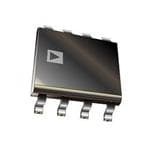
| 描述 | IC MAGNETIC FIELD SNSR LIN 8SOIC板机接口霍耳效应/磁性传感器 IC Linear Output Magnetic Field Sensr |
| 产品分类 | 磁性传感器 - 霍尔效应,数字开关,线性,罗盘 (IC)磁性传感器 |
| 品牌 | Analog Devices Inc |
| 产品手册 | |
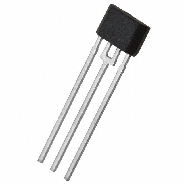
| 产品图片 |
|
| rohs | 符合RoHS无铅 / 符合限制有害物质指令(RoHS)规范要求 |
| 产品系列 | 板机接口霍耳效应/磁性传感器,Analog Devices AD22151YRZ- |
| 数据手册 | |
| 产品型号 | AD22151YRZ |
| 产品目录页面 | |
| 产品种类 | 板机接口霍耳效应/磁性传感器 |
| 供应商器件封装 | 8-SOIC |
| 功率耗散 | 25 mW |
| 包装 | 管件 |
| 商标 | Analog Devices |
| 安装风格 | SMD/SMT |
| 封装 | Tube |
| 封装/外壳 | 8-SOIC(0.154",3.90mm 宽) |
| 封装/箱体 | SOIC-8 |
| 工作温度 | -40°C ~ 150°C |
| 工作电源电压 | 5 V |
| 工厂包装数量 | 98 |
| 感应范围 | 无限制 |
| 最大工作温度 | + 150 C |
| 最大输出电流 | 0.001 A |
| 最小工作温度 | - 40 C |
| 标准包装 | 98 |
| 特性 | - |
| 电压-电源 | 4.5 V ~ 6 V |
| 电流-电源 | 10mA |
| 电流-输出(最大值) | 15mA |
| 电源电压-最大 | 6 V |
| 电源电压-最小 | 4.5 V |
| 电源电流 | 0.006 A |
| 类型 | 线性 - 单极,双极 |
| 系列 | AD22151G |
| 输出电压 | 1 V |
| 输出类型 | 模拟,比率 |


- 商务部:美国ITC正式对集成电路等产品启动337调查
- 曝三星4nm工艺存在良率问题 高通将骁龙8 Gen1或转产台积电
- 太阳诱电将投资9.5亿元在常州建新厂生产MLCC 预计2023年完工
- 英特尔发布欧洲新工厂建设计划 深化IDM 2.0 战略
- 台积电先进制程称霸业界 有大客户加持明年业绩稳了
- 达到5530亿美元!SIA预计今年全球半导体销售额将创下新高
- 英特尔拟将自动驾驶子公司Mobileye上市 估值或超500亿美元
- 三星加码芯片和SET,合并消费电子和移动部门,撤换高东真等 CEO
- 三星电子宣布重大人事变动 还合并消费电子和移动部门
- 海关总署:前11个月进口集成电路产品价值2.52万亿元 增长14.8%


PDF Datasheet 数据手册内容提取
Linear Output Magnetic Field Sensor AD22151 FEATURES FUNCTIONAL BLOCK DIAGRAM Adjustable Offset to Unipolar or Bipolar Operation Low Offset Drift over Temperature Range Gain Adjustable over Wide Range REF Low Gain Drift over Temperature Range VCC/2 Adjustable First Order Temperature Compensation TEMP REF Ratiometric to VCC OUT AMP AD22151 APPLICATIONS Automotive ISOURCE Throttle Position Sensing Pedal Position Sensing Suspension Position Sensing SWITCHES DEMOD Valve Position Sensing Industrial Absolute Position Sensing Proximity Sensing VCC GENERAL DESCRIPTION NC The AD22151 is a linear magnetic field transducer. The sensor output is a voltage proportional to a magnetic field applied R1 R2 perpendicularly to the package top surface. The sensor combines integrated bulk Hall cell technology and 0.1(cid:1)F instrumentation circuitry to minimize temperature related drifts associated with silicon Hall cell characteristics. The architecture R3 maximizes the advantages of a monolithic implementation while OUTPUT allowing sufficient versatility to meet varied application require- ments with a minimum number of components. NC = NO CONNECT AD22151 Principal features include dynamic offset drift cancellation GND and a built-in temperature sensor. Designed for single 5 V Figure 1.Typical Bipolar Configuration with Low supply operation, the AD22151 achieves low drift offset and (< –500 ppm) Compensation gain operation over –40∞C to +150∞C. Temperature compensa- tion can accommodate a number of magnetic materials commonly utilized in economic position sensor assemblies. VCC The transducer can be configured for specific signal gains to R1 meet various application requirements. Output voltage can be adjusted from fully bipolar (reversible) field operation to fully R4 unipolar field sensing. NC R2 The voltage output achieves near rail-to-rail dynamic range, 0.1(cid:1)F capable of supplying 1 mA into large capacitive loads. The R3 signal is ratiometric to the positive supply rail in all configurations. OUTPUT NC = NO CONNECT AD22151 GND Figure 2.Typical Unipolar Configuration with High ((cid:1) –2000 ppm) Compensation REV.A Information furnished by Analog Devices is believed to be accurate and reliable. However, no responsibility is assumed by Analog Devices for its use, nor for any infringements of patents or other rights of third parties that may result from its use. No license is granted by implication or otherwise One Technology Way, P.O. Box 9106, Norwood, MA 02062-9106, U.S.A. under any patent or patent rights of Analog Devices. Trademarks and Tel: 781/329-4700 www.analog.com registered trademarks are the property of their respective companies. Fax: 781/326-8703 © 2003 Analog Devices, Inc. All rights reserved.
AD22151–SPECIFICATIONS (T = 25(cid:2)C and V+ = 5 V, unless otherwise noted.) A Parameter Min Typ Max Unit OPERATION V Operating 4.5 5.0 6.0 V CC I Operating 6.0 10 mA CC INPUT TC3 (Pin 3) Sensitivity/Volt 160 mV/G/V V Input Range1 CC ±0.5 V 2 OUTPUT2 Sensitivity (External Adjustment, Gain = +1) 0.4 mV/G Linear Output Range 10 90 % of V CC Output Min 5.0 % of V CC Output Max (Clamp) 93 % of V CC Drive Capability 1.0 mA V Offset @ 0 Gauss CC V 2 Offset Adjust Range 5.0 95 % of V CC Output Short Circuit Current 5.0 mA ACCURACIES Nonlinearity (10% to 90% Range) 0.1 % FS Gain Error (Over Temperature Range) ±1 % Offset Error (Over Temperature Range) ±6.0 G Uncompensated Gain TC (G ) 950 ppm TCU RATIOMETRICITY ERROR 1.0 %V/V CC 3 dB ROLL-OFF (5 mV/G) 5.7 kHz OUTPUT NOISE FIGURE (6 kHz BW) 2.4 mV/rms PACKAGE 8-Lead SOIC OPERATING TEMPERATURE RANGE –40 +150 ∞C NOTES 1–40∞C to +150∞C. 2RL = 4.7 kW. Specifications subject to change without notice. ABSOLUTE MAXIMUM RATINGS* ORDERING GUIDE Supply Voltage . . . . . . . . . . . . . . . . . . . . . . . . . . . . . . . . . .12 V Temperature Package Package Package Power Dissipation . . . . . . . . . . . . . . . . . . . . . .25 mW Model Range Description Option Storage Temperature . . . . . . . . . . . . . . . . . . .–50∞C to +160∞C Output Sink Current, IO . . . . . . . . . . . . . . . . . . . . . . . . 15 mA AD22151YR –40∞C to +150∞C 8-Lead SOIC R-8 Magnetic Flux Density . . . . . . . . . . . . . . . . . . . . . . Unlimited AD22151YR-REEL –40∞C to +150∞C 8-Lead SOIC R-8 Lead Temperature (Soldering 10 sec) . . . . . . . . . . . . . . 300∞C *Stresses above those listed under Absolute Maximum Ratings may cause perma- nent damage to the device. This is a stress rating only; functional operation of the device at these or any other conditions above those indicated in the operational sections of this specification is not implied. Exposure to the absolute maximum rating conditions for extended periods may affect device reliability. CAUTION ESD (electrostatic discharge) sensitive device. Electrostatic charges as high as 4000 V readily accumulate on the human body and test equipment and can discharge without detection. Although the AD22151 features proprietary ESD protection circuitry, permanent damage may occur on devices subjected to high energy electrostatic discharges. Therefore, proper ESD precautions are recommended to avoid performance degradation or loss of functionality. –2– REV. A
AD22151 PIN CONFIGURATION PIN FUNCTION DESCRIPTIONS Pin No. Description Connection TC1 1 8 VCC 1 Temperature Compensation 1 Output TC2 2 AD22151 7 REF TOP VIEW 2 Temperature Compensation 2 Output TC3 3 (Not to Scale) 6 GAIN GND 4 5 OUTPUT 3 Temperature Compensation 3 Input/Output 4 Ground AREA OF SENSITIVITY* 5 Output Output 1 8 6 Gain Input 2 7 7 Reference Output 3 6 (Not to Scale) 8 Positive Power Supply 4 5 *SHADED AREA REPRESENTS MAGNETIC FIELD AREA OF SENSITIVITY (20MILS (cid:3) 20MILS) POSITIVE B FIELD INTO TOP OF PACKAGE RESULTS IN A POSITIVE VOLTAGE RESPONSE CIRCUIT OPERATION “valleys” of the silicon crystal. Mechanical force on the sensor is The AD22151 consists of epi Hall plate structures located at the attributable to package-induced stress. The package material center of the die. The Hall plates are orthogonally sampled by acts to distort the encapsulated silicon, altering the Hall cell commutation switches via a differential amplifier. The two gain by ±2% and GTCU by ±200 ppm. amplified Hall signals are synchronously demodulated to provide a Figure 4 shows the typical G characteristic of the AD22151. resultant offset cancellation (see Figure 3). The demodulated TCU This is the observable alteration of gain with respect to tempera- signal passes through a noninverting amplifier to provide final ture with Pin 3 (TC3) held at a constant 2.5 V (uncompensated). gain and drive capability. The frequency at which the output If a permanent magnet source used in conjunction with the signal is refreshed is 50 kHz. sensor also displays an intrinsic TC (B ), it will require factoring TC 0.005 into the total temperature compensation of the sensor assembly. Figures 5 and 6 represent typical overall temperature/gain per- 0.004 formance for a sensor and field combination (B = –200 ppm). TC 0.003 Figure 5 is the total drift in volts over a –40∞C to +150∞C tem- 0.002 perature range with respect to applied field. Figure 6 represents T – V 0.001 tsyhpoiwca sli mpeilracre dnatatag efo gra ain B var i=a t–io2n00 f0ro pmp m25.∞C. Figures 7 and 8 E TC S F 0 F O 14 –0.001 12 –0.002 10 –0.003 8 –0.004 6 140 120 100 80 60 40 20 0 –20 –40 N TEMPERATURE – (cid:2)C GAI 4 % Figure 3.Relative Quiescent Offset vs. Temperature 2 0 TEMPERATURE DEPENDENCIES The uncompensated gain temperature coefficient (G ) of the –2 TCU AD22151 is the result of fundamental physical properties asso- –4 ciated with silicon bulk Hall plate structures. Low doped Hall –6 plates operated in current bias mode exhibit a temperature –40 10 60 110 160 relationship determined by the action of scattering mechanisms TEMPERATURE – (cid:2)C and doping concentration. Figure 4.Uncompensated Gain Variation (from The relative value of sensitivity to magnetic field can be altered 25∞C) vs. Temperature by the application of mechanical force upon silicon. The mecha- nism is principally the redistribution of electrons throughout the REV. A –3–
AD22151 0.025 2.0 1.8 0.020 1.6 1.4 V – 1.2 L 0.015 A N A SIGN % GAI 10..08 ELT0.010 0.6 D 0.4 0.005 0.2 0 0 –0.2 –600 –400 –200 0 200 400 600 –40 10 60 110 160 FIELD – Gauss TEMPERATURE – (cid:2)C Figure 5.Signal Drift over Temperature (–40∞C to Figure 8.Gain Variation (from 25∞C) vs. Temperature +150∞C) vs. Field (–200 ppm); 5 V Supply (–2000 ppm Field; R1 = 12 kW) 0.25 TEMPERATURE COMPENSATION The AD22151 incorporates a “thermistor” transducer that 0.20 detects relative chip temperature within the package. This function provides a compensation mechanism for the various temperature dependencies of the Hall cell and magnet combina- 0.15 tions. The temperature information is accessible at Pins 1 and AIN 0.10 2 ((cid:1) +2900 ppm/∞C) and Pin 3 ((cid:1) –2900 ppm/∞C), as repre- G sented by Figure 9. The compensation voltages are trimmed % to converge at VCC/2 at 25∞C. Pin 3 is internally connected to 0.05 the negative TC voltage via an internal resistor (see the Func- tional Block Diagram). An external resistor connected between 0 Pin 3 and Pins 1 or 2 will produce a potential division of the two complementary TC voltages to provide optimal compensa- –0.05 tion. The Pin 3 internal resistor provides a secondary TC –40 10 60 110 160 TEMPERATURE – (cid:2)C designed to reduce second order Hall cell temperature sensitivity. Figure 6.Gain Variation from 25∞C vs. Temperature 1.0 (–200 ppm) Field; R1 –15 kW 0.8 0.045 0.6 TC1, TC2 VOLTS 0.040 0.4 e c 0.035 eren 0.2 SIGNAL – V00..003205 VOLTS – Ref––00..024 TC3 VOLTS A 0.020 LT –0.6 E D0.015 –0.8 0.010 –1.0 150 112 74 36 –2 –40 0.005 TEMPERATURE – (cid:2)C 0 Figure 9.TC1, TC2, and TC3 with Respect to Reference –800 –600 –400 –200 0 200 400 600 800 FIELD – Gauss vs. Temperature Figure 7.Signal Drift over Temperature (–40∞C to The voltages present at Pins 1, 2, and 3 are proportional to the +150∞C) vs. Field (–2000 ppm); 5 V Supply supply voltage. The presence of the Pin 2 internal resistor dis- tinguishes the effective compensation ranges of Pins 1 and 2. (See temperature configuration in Figures 1 and 2, and typical resistor values in Figures 10 and 11.) Variation occurs in the operation of the gain temperature com- pensation for two reasons. First, the die temperature within the package is somewhat higher than the ambient temperature due –4– REV. A
AD22151 to self-heating as a function of power dissipation. Second, pack- 800 age stress effect alters the specific operating parameters of the gain compensation, particularly the specific crossover tempera- 600 ture of TC1, TC3 ( (cid:1) ±10∞C). 400 CONFIGURATION AND COMPONENT SELECTION m There are three areas of sensor operation that require external pp 200 – component selection: temperature compensation (R1), signal T gain (R2 and R3), and offset (R4). RIF 0 D Temperature –200 If the internal gain compensation is used, an external resistor is required to complete the gain TC circuit at Pin 3. A number of –400 factors contribute to the value of this resistor: –600 a. The intrinsic Hall cell sensitivity TC (cid:1) 950 ppm. 0 5 10 15 20 25 30 35 40 45 50 b. Package induced stress variation in a. (cid:1) ±150 ppm. R1 – k(cid:4) c. Specific field TC (cid:1) –200 ppm (Alnico), –2000 ppm Figure 11.Drift Compensation (Pins 2 and 3) vs. (Ferrite), 0 ppm (electromagnet), and so on. Typical Resistor Value R1 d. R1, TC. GAIN AND OFFSET The final value of target compensation also dictates the use of The operation of the AD22151 can be bipolar (i.e., 0 Gauss = either Pin 1 or Pin 2. Pin 1 is provided to allow for large nega- V /2), or a ratiometric offset can be implemented to position tive field TC devices such as ferrite magnets; thus, R1 would be CC Zero Gauss point at some other potential (i.e., 0.25 V). connected to Pins 1 and 3. The gain of the sensor can be set by the appropriate R2 and R3 Pin 2 uses an internal resistive TC to optimize smaller field resistor values (see Figure 1) such that: coefficients such as Alnico down to 0 ppm coefficients when only the sensor gain TC itself is dominant. Because the TC of R3 R1 itself will also affect the compensation, a low TC resistor G ain=1+ R2 ¥0.4mV /G (1) (±50 ppm) is recommended. However, if an offset is required to position the quiescent out- Figures 10 and 11 indicate R1 resistor values and their associ- put at some other voltage, the gain relationship is modified to: ated effectiveness for Pins 1 and 2, respectively. Note that the indicated drift response in both cases incorporates the intrinsic R3 Hall sensitivity TC (BTCU). G ain=1+ (R2R4)¥0.4mV /G (2) For example, the AD22151 sensor is to be used in conjunction The offset that R4 introduces is: with an Alnico material permanent magnet. The TC of such mag- nets is (cid:1) –200 ppm (see Figures 5 and 6). Figure 11 indicates R3 that a compensating drift of 200 ppm at Pin 3 requires a nomi- O ffset =1+ (R2+R4)¥(VCC –VOUT) (3) nal value of R1 = 18 kW (assuming negligible drift of R1 itself). For example, at V = 5 V at room temperature, the internal gain of CC 3500 the sensor is approximately 0.4 mV/Gauss. If a sensitivity of 6 mV/Gauss is required with a quiescent output voltage of 1 V, 3000 the calculations below apply (see Figure 2). A value would be selected for R3 that complied with the various 2500 considerations of current and power dissipation, trim ranges (if m applicable), and so on. For the purpose of example, assume a p2000 – p value of 85 kW. T RIF1500 To achieve a quiescent offset of 1 V requires a value for R4 as: D 1000 ÊVCCˆ –1 500 ËÁ 2 ¯˜ =0.375 (4) V CC 0 Thus: 0 5 10 15 20 25 30 R1 – k(cid:4) Ê85kWˆ Figure 10.Drift Compensation (Pins 1 and 3) vs. R4=Á ˜ –85kW=141.666kW (5) Typical Resistor Value R1 Ë0.375¯ The gain required would be 6/0.4 (mV/Gauss) = 15. REV. A –5–
AD22151 Knowing the values of R3 and R4 and noting Equation 2, the 7 parallel combination of R2 and R4 required is: 6 85kΩ ( ) =6.071kΩ 3dB FREQUENCY (kHz) 15–1 5 Hz k Thus: Y – 4 C N E QU 3 E R2= 1 =6.342kΩ FR 2 1 1 – 1 6.071kΩ 141.666kΩ 0 1 2 3 4 5 6 NOISE GAIN – mV/Gauss The principal noise component in the sensor is thermal noise Figure 13.Small Signal Gain Bandwidth vs. Gain from the Hall cell. Clock feedthrough into the output signal is largely suppressed with application of a supply bypass capacitor. 3ACQS TEK STOP: 25.0 kS/s [ T [ Figure 12 shows the power spectral density (PSD) of the output signal for a gain of 5 mV/Gauss. The effective bandwidth of the sensor is approximately 5.7 kHz, as shown in Figure 13. The CH2 p-p 19.2mV PSD indicates an rms noise voltage of 2.8 mV within the 3 dB bandwidth of the sensor. A wideband measurement of 250 MHz indicates 3.2 mV rms (see Figure 14a). In many position sensing applications, bandwidth requirements can be as low as 100 Hz. Passing the output signal through a 100 Hz LP filter, for example, would reduce the rms noise volt- age to (cid:1)1 mV. A dominant pole may be introduced into the output amplifier response by connection of a capacitor across feedback resistor R3 as a simple means of reducing noise at the expense of bandwidth. Figure 14b indicates the output signal of CH2 10.0mV BW M2.00ms a 5 mV/G sensor bandwidth limited to 180 Hz with a 0.01 µF Figure 14a.Peak-to-Peak Full Bandwidth (10 mV/Division) feedback capacitor. Note: Measurements were taken with a 0.1 µF decoupling 7ACQS capacitor between V and GND at 25°C. TEK STOP: 25.0 kS/s [ T [ CC B MARKER (cid:2) 64Hz Y: 3.351(cid:1)H CH2 p-p 100(cid:1)H 4.4mV LOGMAG 5 dB/div CH2 10.0mV BWM2.00ms Figure 14b.Peak-to-Peak 180 Hz Bandwidth (10 mV/Division) 1(cid:1)H START: 64Hz STOP: 25.6kHz NOISE: PSD (8mV/GAUSS) RMS: 64 Figure 12.Power Spectral Density (5 mV/G) –6– REV. A
AD22151 0.06 2.496 0.05 2.494 0.04 0.03 2.492 0.02 R O 0.01 S % ERR 0 VOLT 2.490 GAIN = 3.78mV/G –0.01 2.488 –0.02 –0.03 2.486 –0.04 –0.05 2.484 –600 –400 –200 0 200 400 600 140 120 100 80 60 40 20 0 –20 –40 FIELD – Gauss TEMPERATURE – (cid:2)C Figure 15.Integral Nonlinearity vs. Field Figure 16.Absolute Offset Volts vs. Temperature OUTLINE DIMENSIONS 8-Lead Standard Small Outline Package [SOIC] Narrow Body (R-8) Dimensions shown in millimeters and (inches) 5.00 (0.1968) 4.80 (0.1890) 8 5 4.00 (0.1574) 6.20 (0.2440) 3.80 (0.1497) 1 4 5.80 (0.2284) 1.27B (0S.C0500) 1.75 (0.0688) 00..5205 ((00..00109969))(cid:3) 45(cid:2) 0.25 (0.0098) 1.35 (0.0532) 0.10 (0.0040) 0.51 (0.0201) 8(cid:2) COPLANARITY 0.33 (0.0130) 0.25 (0.0098)0(cid:2) 1.27 (0.0500) 0.10 SEPALTAINNGE 0.19 (0.0075) 0.41 (0.0160) COMPLIANT TO JEDEC STANDARDS MS-012AA CONTROLLING DIMENSIONS ARE IN MILLIMETERS; INCH DIMENSIONS (IN PARENTHESES) ARE ROUNDED-OFF MILLIMETER EQUIVALENTS FOR REFERENCE ONLY AND ARE NOT APPROPRIATE FOR USE IN DESIGN REV. A –7–
AD22151 Revision History Location Page 2/03—Data Sheet changed from REV. 0 to REV. A. Change to ORDERING GUIDE . . . . . . . . . . . . . . . . . . . . . . . . . . . . . . . . . . . . . . . . . . . . . . . . . . . . . . . . . . . . . . . . . . . . . . . . . . . .2 Updated OUTLINE DIMENSIONS . . . . . . . . . . . . . . . . . . . . . . . . . . . . . . . . . . . . . . . . . . . . . . . . . . . . . . . . . . . . . . . . . . . . . . . .7 A) 3( 0 2/ – 0 – 5 7 6 0 0 C A. S. U. N D I E T N RI P –8– REV. A
Mouser Electronics Authorized Distributor Click to View Pricing, Inventory, Delivery & Lifecycle Information: A nalog Devices Inc.: AD22151YRZ AD22151YRZ-RL