ICGOO在线商城 > 分立半导体产品 > 晶闸管 - TRIAC > ACST410-8BTR

 Datasheet下载
- 型号: ACST410-8BTR
- 制造商: STMicroelectronics
- 库位|库存: xxxx|xxxx
- 要求:
| 数量阶梯 | 香港交货 | 国内含税 |
| +xxxx | $xxxx | ¥xxxx |
查看当月历史价格
查看今年历史价格
ACST410-8BTR产品简介:
ICGOO电子元器件商城为您提供ACST410-8BTR由STMicroelectronics设计生产,在icgoo商城现货销售,并且可以通过原厂、代理商等渠道进行代购。 ACST410-8BTR价格参考¥6.28-¥6.28。STMicroelectronicsACST410-8BTR封装/规格:晶闸管 - TRIAC, TRIAC Logic - Sensitive Gate 800V 4A Surface Mount DPAK。您可以下载ACST410-8BTR参考资料、Datasheet数据手册功能说明书,资料中有ACST410-8BTR 详细功能的应用电路图电压和使用方法及教程。
STMicroelectronics的ACST410-8BTR是一款800V高阻断电压的TRIAC,属于晶闸管器件,专为交流电源控制设计。该器件采用SOT-223封装,具有良好的热性能和紧凑尺寸,适用于空间受限的高可靠性应用。

典型应用场景包括:家用电器中的交流负载控制,如电饭煲、电磁炉、洗衣机和空调的加热或电机驱动模块;工业自动化中的固态继电器(SSR)、小型电机调速与开关控制;照明系统中用于调光器电路,特别是白炽灯或卤素灯的相位控制调光;还可用于电源开关、温控器及智能插座等需要直接控制交流市电的场合。

ACST410-8BTR具备高抗干扰能力和良好的dV/dt性能,适合在存在电压瞬变的电网环境中稳定工作。其无铅环保设计符合RoHS标准,适用于现代绿色电子产品。由于其灵敏栅极触发特性,可直接由微控制器或光耦驱动,简化了驱动电路设计,提升了系统集成度与可靠性。

综上,ACST410-8BTR广泛应用于需安全、高效控制交流负载的消费电子、工业控制和智能家居系统中。
| 参数 | 数值 |
| 产品目录 | |
| 描述 | TRIAC SENS GATE 800V 4A DPAK双向可控硅 Overvoltage Triac Low <10mA 1500 rms |
| 产品分类 | 双向可控硅分离式半导体 |
| GateTriggerCurrent-Igt | 10 mA |
| GateTriggerVoltage-Vgt | 1 V |
| 品牌 | STMicroelectronics |
| 产品手册 | |
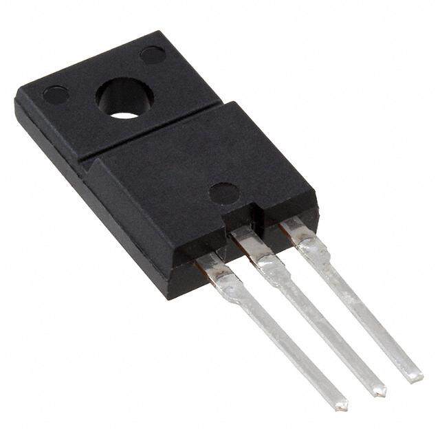
| 产品图片 |
|
| rohs | 符合RoHS无铅 / 符合限制有害物质指令(RoHS)规范要求 |
| 产品系列 | 晶体闸流管,双向可控硅,STMicroelectronics ACST410-8BTRACS™/A.S.D® |
| 数据手册 | |
| 产品型号 | ACST410-8BTR |
| 三端双向可控硅类型 | 逻辑 - 灵敏栅极 |
| 产品培训模块 | http://www.digikey.cn/PTM/IndividualPTM.page?site=cn&lang=zhs&ptm=26297http://www.digikey.cn/PTM/IndividualPTM.page?site=cn&lang=zhs&ptm=26298 |
| 产品种类 | 双向可控硅 |
| 供应商器件封装 | D-Pak |
| 保持电流Ih最大值 | 20 mA |
| 关闭状态漏泄电流(在VDRMIDRM下) | 40 mA |
| 其它名称 | 497-10557-6 |
| 其它有关文件 | http://www.st.com/web/catalog/sense_power/FM144/CL1208/SC1420/PF62672?referrer=70071840 |
| 包装 | Digi-Reel® |
| 商标 | STMicroelectronics |
| 安装类型 | 表面贴装 |
| 安装风格 | SMD/SMT |
| 封装 | Reel |
| 封装/外壳 | TO-252-3,DPak(2 引线+接片),SC-63 |
| 封装/箱体 | DPAK |
| 工厂包装数量 | 2500 |
| 开启状态RMS电流-ItRMS | 4 A |
| 栅极触发电压-Vgt | 1 V |
| 栅极触发电流-Igt | 10 mA |
| 标准包装 | 1 |
| 电压-断态 | 800V |
| 电压-栅极触发(Vgt)(最大值) | 1V |
| 电流-不重复浪涌50、60Hz(Itsm) | 30A,32A |
| 电流-保持(Ih)(最大值) | 20mA |
| 电流-栅极触发(Igt)(最大值) | 10mA |
| 电流-通态(It(RMS))(最大值) | 4A |
| 系列 | ACST4 |
| 配置 | 单一 |
| 额定重复关闭状态电压VDRM | 800 V |


- 商务部:美国ITC正式对集成电路等产品启动337调查
- 曝三星4nm工艺存在良率问题 高通将骁龙8 Gen1或转产台积电
- 太阳诱电将投资9.5亿元在常州建新厂生产MLCC 预计2023年完工
- 英特尔发布欧洲新工厂建设计划 深化IDM 2.0 战略
- 台积电先进制程称霸业界 有大客户加持明年业绩稳了
- 达到5530亿美元!SIA预计今年全球半导体销售额将创下新高
- 英特尔拟将自动驾驶子公司Mobileye上市 估值或超500亿美元
- 三星加码芯片和SET,合并消费电子和移动部门,撤换高东真等 CEO
- 三星电子宣布重大人事变动 还合并消费电子和移动部门
- 海关总署:前11个月进口集成电路产品价值2.52万亿元 增长14.8%

PDF Datasheet 数据手册内容提取
ACST4 Overvoltage protected AC switch Datasheet - production data Description The ACST4 series belongs to the ACS / ACST OUT power switch family. This high performance device is suited to home appliances or industrial systems and drives loads up to 4 A. This ACST4 switch embeds a Triac structure with G COM OUT a high voltage clamping device to absorb the G COM inductive turn-off energy and withstand line DPAK TO-220FPAB transients such as those described in the IEC61000-4-5 standards. The ACST410 needs a low gate current to be activated (I < 10 mA) and GT still shows a high electrical noise immunity Features complying with IEC standards such as IEC61000-4-4 (fast transient burst test). • Triac with overvoltage protection • Low I (<10 mA) or high immunity Figure 1. Functional diagram GT (I < 35 mA) version OUT GT • High noise immunity: static dV/dt > 1000 V/µs • TO-220FPAB insulated package: – complies with UL standards (File ref : E81734) – insulation voltage: 2000 V RMS G Benefits COM • Enables equipment to meet IEC 61000-4-5 • High off-state reliability with planar technology Table 1. Device summary • Needs no external overvoltage protection Symbol Value Unit • Reduces the power passive component count I 4 A T(RMS) • High immunity against fast transients V /V 800 V described in IEC 61000-4-4 standards DRM RRM I (ACST410) 10 mA GT Applications I (ACST435) 35 mA GT • AC mains static switching in appliance and industrial control systems • Drive of medium power AC loads such as: – Universal motor of washing machine drum – Compressor for fridge or air conditioner May 2017 DocID8766 Rev 8 1/14 This is information on a product in full production. www.st.com
Characteristics ACST4 1 Characteristics Table 2. Absolute maximum ratings (limiting values) Symbol Parameter Value Unit TO-220FPAB T = 102 °C c 4 DPAK T = 112 °C I On-state rms current (full sine wave) c A T(RMS) DPAK with 0.5 T = 60 °C 1 cm² copper amb Non repetitive surge peak on-state current F = 60 Hz tp = 16.7 ms 32 A I TSM (full cycle sine wave, TJ initial = 25 °C) F = 50 Hz tp = 20 ms 30 A I²t I²t Value for fusing t = 10 ms 6 A²s p Critical rate of rise of on-state current dI/dt F = 120 Hz T = 125 °C 100 A/µs I = 2 x I , t = 100 ns j G GT r V (1) Non repetitive line peak mains voltage (1) T = 25 °C 2 kV PP j P Average gate power dissipation T = 125 °C 0.1 W G(AV) j P Peak gate power dissipation (t = 20 µs) T = 125 °C 10 W GM p j I Peak gate current (t = 20 µs) T = 125 °C 1.6 A GM p j T Storage junction temperature range -40 to +150 stg °C T Operating junction temperature range -40 to +125 j T Maximum lead soldering temperature during 10 s (at 3 mm from plastic case) 260 °C l V Insulation RMS voltage (60 seconds) T0-220FPAB 2000 V INS(RMS) 1. According to test described in IEC 61000-4-5 standard and Figure18 T able 3. Electrical characteristics (T = 25 °C, unless otherwise specified) j Symbol Test conditions Quadrant ACST410 ACST435 Unit I (1) V = 12 V, R = 33 Ω I - II - III MAX 10 35 mA GT OUT L V V = 12 V, R = 33 Ω I - II - III MAX 1.0 1.1 V GT OUT L V V = V , R = 3.3 kΩ,T = 125 °C I - II - III MIN 0.2 V GD OUT DRM L j I (2) I = 500 mA MAX 20 25 mA H OUT I I = 1.2 x I I - II-III MAX 40 60 mA L G GT dV/dt (2) V = 67% V gate open, T = 125 °C MIN 500 1000 V/µs OUT DRM j (dI/dt)c (2) without snubber, T = 125 °C MIN 5 A/ms j (dI/dt)c (2) (dV/dt)c = 15 V/µs, T = 125 °C MIN 2 A/ms j V I = 0.1 mA, t = 1 ms MIN 850 V CL CL p 1. Minimum I is guaranteed at 5% of I max GT GT 2. For both polarities of OUT pin referenced to COM pin 2/14 DocID8766 Rev 8
ACST4 Characteristics Table 4. Static electrical characteristics Symbol Test conditions Value Unit V (1) I = 5.6 A, t = 500 µs T = 25 °C MAX 1.7 V TM TM p j V (1) Threshold voltage T = 125 °C MAX 0.9 V TO j R (1) Dynamic resistance T = 125 °C MAX 110 mΩ D j IDRM V = V / V Tj = 25 °C MAX 20 µA IRRM OUT DRM RRM Tj = 125 °C 0.5 mA 1. For both polarities of OUT pin referenced to COM pin Table 5. Thermal resistances Symbol Parameter Value Unit DPAK 2.6 R Junction to case for full cycle sine wave conduction th(j-c) TO-220FPAB 4.6 °C/W TO-220FPAB 60 R Junction to ambient th(j-a) S (1)= 0.5 cm² DPAK 70 CU 1. S = copper surface under tab CU Figure 2. M a ximum power dissipation versus Figure 3. On-state RMS current versus case on-state RMS current temperature (full cycle) 6 P(W) IT(RMS)(A) α= 180° 180° 5 α=180° 5 DPAK 4 TO220FPAB 4 3 3 2 2 1 1 IT(RMS)(A) TC(°C) 0 0 0.0 0.5 1.0 1.5 2.0 2.5 3.0 3.5 4.0 0 25 50 75 100 125 DocID8766 Rev 8 3/14 14
Characteristics ACST4 Figure 4. On -state RMS current versus ambient Figure 5. Relative variation of thermal temperature (free air convection, full cycle) impedance versus pulse duration IT(RMS)(A) K = [Zth/ Rth] 2.0 1.0E+00 α=180° Zth(j-c) TO-220FPAB DPAK Zth(j-a) 1.5 DPAKwithcopper surface = 0.5 cm2 1.0 1.0E-01 TO-220FPAB 0.5 Ta(°C) Tp(s) 0.0 1.0E-02 0 25 50 75 100 125 1.0E-03 1.0E-02 1.0E-01 1.0E+00 1.0E+01 1.0E+02 1.0E+03 Figure 6. R elative variation of gate trigger Figure 7. Relative variation of holding current current (I ) and voltage (V ) versus junction (I ) and latching current (I ) versus junction GT GT H L temperature (typical values) temperature (typical values) 3.0 IGT,VGT[Tj] / IGT,VGT[Tj= 25 °C ] 2.5 IH,IL[Tj] / IH,IL[Tj= 25 °C] 2.5 IGT Q3 2.0 2.0 IGT Q1-Q2 1.5 1.5 1.0 1.0 VGTQ1-Q2-Q3 IL 0.5 0.5 IH Tj(°C) Tj(°C) 0.0 0.0 -50 -25 0 25 50 75 100 125 -50 -25 0 25 50 75 100 125 Figure 8 . Surge peak on-state current Figure 9. Non repetitive surge peak on-state versus number of cycles current versus sinusoidal pulse width ITSM(A) ITSM(A), (A2s) 35 1000 dl /dt limitation: 100 A / μs Tjinitial = 25 °C 30 t=20ms 25 Nonrepetitive One cycle 100 Tjinitial=25°C ITSM 20 15 10 10 Repetitive 5 TC=102°C Number of cycles t (ms) p 0 1 1 10 100 1000 0.01 0.10 1.00 10.00 4/14 DocID8766 Rev 8
ACST4 Characteristics Figur e 10. On-state characteristics Figure 11. Relative variation of critical rate of (maximumvalues) decrease of main current (dI/dt) versus c junction temperature 100 ITM(A) (dI/dt)c[Tj] / (dl/dt)c[Tj= 125 °C] 8 Tjmax: Vto= 0.90V 7 Rd= 110 mΩ 6 5 10 4 3 2 Tj= 125 °C 1 1 Tj= 25 °C VTM(V) 0 Tj(°C) 0 1 2 3 4 5 25 50 75 100 125 Figure 12 . Relative variation of static dV/dt Figure 13. Relative variation of leakage current immunity versus junction temperature versus junction temperature (gateopen) dV/dt [Tj] / dV/dt [Tj= 125 °C] IDRM/IRRM[Tj;VDRM/VRRM] / IDRM/IRRM[Tj= 125 °C;800V] 6 1.0E+00 VD=VR= 536V VDRM=VRRM= 800V 5 Different blocking voltages 4 1.0E-01 VDRM=VRRM= 600V 3 2 1.0E-02 VDRM=VRRM= 200V 1 0 Tj(°C) 1.0E-03 Tj(°C) 25 50 75 100 125 25 50 75 100 125 Figure 14. R elative variation of the clamping Figure 15. Thermal resistance junction to voltage (V ) versus junction temperature ambient versus copper surface under tab CL (minimum values) 1.15 VCL[Tj] /VCL[Tj= 25 °C] (cid:27)(cid:19) (cid:53)(cid:87)(cid:75)(cid:11)(cid:77)(cid:16)(cid:68)(cid:12)(cid:11)(cid:131)(cid:38)(cid:18)(cid:58)(cid:12) (cid:26)(cid:19) 1.10 (cid:25)(cid:19) 1.05 (cid:24)(cid:19) 1.00 (cid:23)(cid:19) (cid:22)(cid:19) 0.95 (cid:21)(cid:19) 0.90 (cid:40)(cid:83)(cid:82)(cid:91)(cid:92)(cid:83)(cid:85)(cid:76)(cid:81)(cid:87)(cid:72)(cid:71)(cid:69)(cid:82)(cid:68)(cid:85)(cid:71)(cid:41)(cid:53)(cid:23)(cid:15)(cid:72)(cid:38)(cid:56)(cid:32)(cid:22)(cid:24)(cid:151)(cid:80) (cid:20)(cid:19) Tj(°C) (cid:54)(cid:38)(cid:88)(cid:11)(cid:70)(cid:80)(cid:240)(cid:12) 0.85 (cid:19) -50 -25 0 25 50 75 100 125 (cid:19) (cid:24) (cid:20)(cid:19) (cid:20)(cid:24) (cid:21)(cid:19) (cid:21)(cid:24) (cid:22)(cid:19) (cid:22)(cid:24) (cid:23)(cid:19) DocID8766 Rev 8 5/14 14
Application information ACST4 2 Application information 2.1 Typical application description The ACST4 device has been designed to control medium power load, such as AC motors in home appliances. Thanks to its thermal and turn off commutation performances, the ACST4 switch is able to drive an inductive load up to 4 A with no turn off additional snubber. It also provides high thermal performances in static and transient modes such as the compressor inrush current or high torque operating conditions of an AC motor. Thanks to its low gate triggering current level, the ACST4 can be driven directly by an MCU through a simple gate resistor as shown Figure16 and Figure17. Figure 16. Compressor control – typical diagrams Compressor Compressor AC Mains AC Mains PTC Electronic PTC ACST starter 2 1 logical circuitry ACST Start 3 switch ACST Run switch Electronic ACST thermostat Rg Rg Rg Gate Gate Driver Power supply Driver Power supply Compressor with integrated e-starter Compressor with external electronic drive 6/14 DocID8766 Rev 8
ACST4 Application information Figure 17. Universal drum motor control – typical diagram Universal motor Stator Rotor 12V AC Mains Motor direction setting MCU Speed motor ACST Rg regulation Vcc MCU 2.2 AC line transient voltage ruggedness In comparison with standard Triacs, which are not robust against surge voltage, the ACST4 is self-protected against over-voltage, specified by the new parameter V . The ACST4 CL switch can safely withstand AC line transient voltages either by clamping the low energy spikes, such as inductive spikes at switch off, or by switching to the on state (for less than 10 ms) to dissipate higher energy shocks through the load. This safety feature works even with high turn-on current ramp up. The test circuit of Figure18 represents the ACST4 application, and is used to stress the ACST switch according to the IEC 61000-4-5 standard conditions. With the additional effect of the load which is limiting the current, the ACST switch withstands the voltage spikes up to 2 kV on top of the peak line voltage. The protection is based on an overvoltage crowbar technology. The ACST4 folds back safely to the on state as shown in Figure19. The ACST4 recovers its blocking voltage capability after the surge and the next zero current crossing. Such a non repetitive test can be done at least 10 times on each AC line voltage polarity. DocID8766 Rev 8 7/14 14
Application information ACST4 Figure 18. Overvoltage ruggedness test circuit for resistive and inductive loads for IEC 61000-4-5 standards R = 23Ω, L = 2 µH,Vsurge = 2 kV Rg = 220Ω(ACST410-8), 68Ω(ACST435-8) Surge generator 2kV surge Rgene Model of the load Filtering unit R L ACST4 AC Mains Rg Figure 19. Typical current and voltage waveforms across the ACST4 during IEC 61000-4-5 standard test Vpeak=VCL 1.2/50 µs voltage surge V 0 Ipeak= 90 A 8/20 µs current surge I 0 dI/dt = 130 A/µs 8/14 DocID8766 Rev 8
ACST4 Package information 3 Package information • Epoxy meets UL94, V0 • Cooling method: by conduction (C) • Recommended torque (TO-220FPAB): 0.4 to 0.6 N·m In order to meet environmental requirements, ST offers these devices in different grades of ECOPACK® packages, depending on their level of environmental compliance. ECOPACK® specifications, grade definitions and product status are available at: www.st.com. ECOPACK® is an ST trademark. Figure 20. TO-220FPAB package outline A H B Dia L6 L2 L7 L3 L5 D F1 L4 F2 F E G1 G DocID8766 Rev 8 9/14 14
Package information ACST4 Table 6. TO-220FPAB package mechanical data Dimensions Ref. Millimeters Inches Min. Typ. Max. Min. Typ. Max. A 4.4 4.6 0.1732 0.1811 B 2.5 2.7 0.0984 0.1063 D 2.5 2.75 0.0984 0.1083 E 0.45 0.70 0.0177 0.0276 F 0.75 1 0.0295 0.0394 F1 1.15 1.70 0.0453 0.0669 F2 1.15 1.70 0.0453 0.0669 G 4.95 5.20 0.1949 0.2047 G1 2.4 2.7 0.0945 0.1063 H 10 10.4 0.3937 0.4094 L2 16 0.6299 L3 28.6 30.6 1.1260 1.2047 L4 9.8 10.6 0.3858 0.4173 L5 2.9 3.6 0.1142 0.1417 L6 15.9 16.4 0.6260 0.6457 L7 9.00 9.30 0.3543 0.3661 Dia. 3.00 3.20 0.1181 0.1260 10/14 DocID8766 Rev 8
ACST4 Package information Figure 21. DPAK package outline (cid:36) (cid:40) (cid:69)(cid:23) (cid:70)(cid:21) (cid:21) (cid:47) (cid:20) (cid:39) (cid:39) (cid:43) (cid:40)(cid:20) (cid:36)(cid:20) (cid:23) (cid:47) (cid:72) (cid:69) (cid:70) (cid:72)(cid:20) (cid:47) (cid:21) (cid:57) (cid:21) (cid:36) Note: This package drawing may slightly differ from the physical package. However, all the specified dimensions are guaranteed. DocID8766 Rev 8 11/14 14
Package information ACST4 Table 7. DPAK package mechanical data Dimensions Ref. Millimeters Inches Min. Typ. Max. Min. Typ. Max. A 2.18 2.40 0.0858 0.0945 A1 0.90 1.10 0.0354 0.0433 A2 0.03 0.23 0.0012 0.0091 b 0.64 0.90 0.0252 0.0354 b4 4.95 5.46 0.1949 0.2150 c 0.46 0.61 0.0181 0.0240 c2 0.46 0.60 0.0181 0.0240 D 5.97 6.22 0.2350 0.2449 D1 4.95 5.60 0.1949 0.2205 E 6.35 6.73 0.2500 0.2650 E1 4.32 5.50 0.1701 0.2165 e 2.286 0.0900 e1 4.40 4.70 0.1732 0.1850 H 9.35 10.40 0.3681 0.4094 L 1.00 1.78 0.0394 0.0701 L2 1.27 0.0500 L4 0.60 1.02 0.0236 0.0402 V2 -8° 8° -8° 8° Figure 22. Footprint (dimensions in mm) 6.7 3.0 3.0 A 5.094 6.7 B 1.6 The device must be positioned within 0.05 AB 12/14 DocID8766 Rev 8
ACST4 Ordering information 4 Ordering information Figure 23. Ordering information scheme ACS T 4 10 - 8 B TR AC switch Topology T =Triac On-state rms current 4 = 4 A Triggering gate current 10 = 10 mA 35 = 35 mA Repetitive peak off-state voltage 8 = 800V Package B = DPAK FP =TO-220FPAB Delivery mode TR =Tape and reel Blank =Tube Table 8. Ordering information Order code Marking Package Weight Base Qty Delivery mode ACST410-8B DPAK 1.5 g 50 Tube ACST410-8BTR ACST4108 DPAK 1.5 g 1000 Tape and reel ACST410-8FP TO-220FPAB 2.4 g 50 Tube ACST435-8B DPAK 1.5 g 50 Tube ACST435-8BTR ACST4358 DPAK 1.5 g 1000 Tape and reel ACST435-8FP TO-220FPAB 2.4 g 50 Tube 5 Revision history Table 9. Document revision history Date Revision Changes Jan-2003 3A Previous update. 04-Jul-2007 4 Reformatted to current standard. Added package. 18-Dec-2009 5 V /V updated to 800 V. Order codes updated. DRM RRM 02-Jun-2014 6 Updated DPAK package information and reformatted to current standard. 21-Oct-2014 7 Updated Table2, Table3,Table4, Features and Description. 18-May-2017 8 Updated Features in cover page, Table2 and Figure14. DocID8766 Rev 8 13/14 14
ACST4 IMPORTANT NOTICE – PLEASE READ CAREFULLY STMicroelectronics NV and its subsidiaries (“ST”) reserve the right to make changes, corrections, enhancements, modifications, and improvements to ST products and/or to this document at any time without notice. Purchasers should obtain the latest relevant information on ST products before placing orders. ST products are sold pursuant to ST’s terms and conditions of sale in place at the time of order acknowledgement. Purchasers are solely responsible for the choice, selection, and use of ST products and ST assumes no liability for application assistance or the design of Purchasers’ products. No license, express or implied, to any intellectual property right is granted by ST herein. Resale of ST products with provisions different from the information set forth herein shall void any warranty granted by ST for such product. ST and the ST logo are trademarks of ST. All other product or service names are the property of their respective owners. Information in this document supersedes and replaces information previously supplied in any prior versions of this document. © 2017 STMicroelectronics – All rights reserved 14/14 DocID8766 Rev 8
Mouser Electronics Authorized Distributor Click to View Pricing, Inventory, Delivery & Lifecycle Information: S TMicroelectronics: ACST4-7SH ACST4-7CH ACST4-7CFP ACST410-8BTR ACST435-8FP ACST410-8B ACST410-8FP ACST435- 8B ACST435-8BTR ACST4-7CB ACST4-7SFP ACST4-7SB-TR ACST4-7CB-TR ACST4-7SB