ICGOO在线商城 > 74LCX541TTR
 Datasheet下载
- 型号: 74LCX541TTR
- 制造商: STMicroelectronics
- 库位|库存: xxxx|xxxx
- 要求:
| 数量阶梯 | 香港交货 | 国内含税 |
| +xxxx | $xxxx | ¥xxxx |
查看当月历史价格
查看今年历史价格
74LCX541TTR产品简介:
ICGOO电子元器件商城为您提供74LCX541TTR由STMicroelectronics设计生产,在icgoo商城现货销售,并且可以通过原厂、代理商等渠道进行代购。 提供74LCX541TTR价格参考以及STMicroelectronics74LCX541TTR封装/规格参数等产品信息。 你可以下载74LCX541TTR参考资料、Datasheet数据手册功能说明书, 资料中有74LCX541TTR详细功能的应用电路图电压和使用方法及教程。
| 参数 | 数值 |
| 产品目录 | 集成电路 (IC)半导体 |
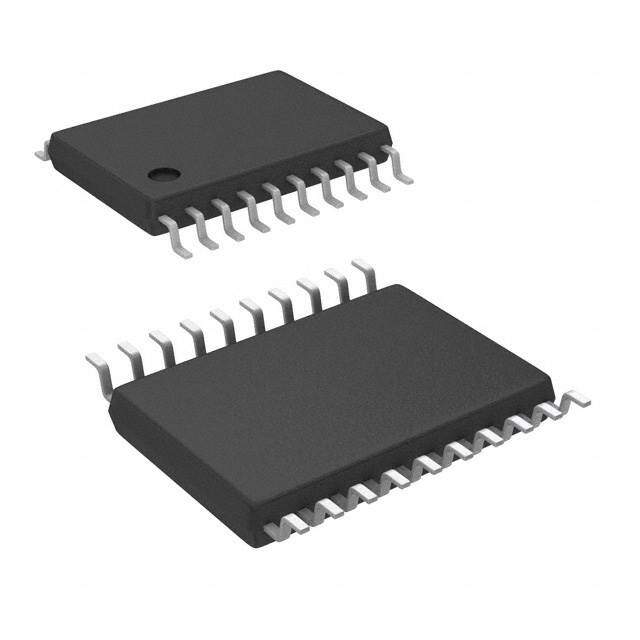
| 描述 | IC BUFF/DVR TRI-ST 8BIT 20TSSOP缓冲器和线路驱动器 Octal Bus Buffer |
| 产品分类 | |
| 品牌 | STMicroelectronics |
| 产品手册 | |
| 产品图片 |
|
| rohs | 符合RoHS无铅 / 符合限制有害物质指令(RoHS)规范要求 |
| 产品系列 | 逻辑集成电路,缓冲器和线路驱动器,STMicroelectronics 74LCX541TTR74LCX |
| 数据手册 | |
| 产品型号 | 74LCX541TTR |
| 产品目录页面 | |
| 产品种类 | 缓冲器和线路驱动器 |
| 传播延迟时间 | 9 ns at 2.7 V, 8 ns at 3 V to 3.6 V |
| 低电平输出电流 | 24 mA |
| 供应商器件封装 | 20-TSSOP |
| 元件数 | 1 |
| 其它名称 | 497-2918-1 |
| 其它有关文件 | http://www.st.com/web/catalog/sense_power/FM140/SC1797/PF62429?referrer=70071840 |
| 包装 | 剪切带 (CT) |
| 商标 | STMicroelectronics |
| 安装类型 | 表面贴装 |
| 安装风格 | SMD/SMT |
| 封装 | Reel |
| 封装/外壳 | 20-TSSOP(0.173",4.40mm 宽) |
| 封装/箱体 | TSSOP-20 |
| 工作温度 | -40°C ~ 85°C |
| 最大工作温度 | + 125 C |
| 最小工作温度 | - 55 C |
| 极性 | Non-Inverting |
| 标准包装 | 1 |
| 每元件位数 | 8 |
| 每芯片的通道数量 | 8 |
| 电压-电源 | 2 V ~ 3.6 V |
| 电流-输出高,低 | 24mA,24mA |
| 电源电压-最大 | 3.6 V |
| 电源电压-最小 | 2 V |
| 系列 | 74LCX541 |
| 输入线路数量 | 8 |
| 输出类型 | 3-State |
| 输出线路数量 | 3 |
| 逻辑类型 | 缓冲器/线路驱动器,非反相 |
| 逻辑系列 | LCX |
| 高电平输出电流 | - 24 mA |


- 商务部:美国ITC正式对集成电路等产品启动337调查
- 曝三星4nm工艺存在良率问题 高通将骁龙8 Gen1或转产台积电
- 太阳诱电将投资9.5亿元在常州建新厂生产MLCC 预计2023年完工
- 英特尔发布欧洲新工厂建设计划 深化IDM 2.0 战略
- 台积电先进制程称霸业界 有大客户加持明年业绩稳了
- 达到5530亿美元!SIA预计今年全球半导体销售额将创下新高
- 英特尔拟将自动驾驶子公司Mobileye上市 估值或超500亿美元
- 三星加码芯片和SET,合并消费电子和移动部门,撤换高东真等 CEO
- 三星电子宣布重大人事变动 还合并消费电子和移动部门
- 海关总署:前11个月进口集成电路产品价值2.52万亿元 增长14.8%


PDF Datasheet 数据手册内容提取
74LCX541 LOW VOLTAGE CMOS OCTAL BUS BUFFER (3-STATE) WITH 5V TOLERANT INPUTS AND OUTPUTS n 5V TOLERANT INPUTS AND OUTPUTS n HIGH SPEED : t = 8.0 ns (MAX.) at V = 3V PD CC n POWER DOWN PROTECTION ON INPUTS AND OUTPUTS n SYMMETRICAL OUTPUT IMPEDANCE: |I | = I = 24mA (MIN) at V = 3V SOP TSSOP OH OL CC n PCI BUS LEVELS GUARANTEED AT 24 mA n BALANCED PROPAGATION DELAYS: t @ t ORDER CODES PLH PHL n OPERATING VOLTAGE RANGE: PACKAGE TUBE T & R V (OPR) = 2.0V to 3.6V (1.5V Data CC SOP 74LCX541M 74LCX541MTR Retention) TSSOP 74LCX541TTR n PIN AND FUNCTION COMPATIBLE WITH 74 SERIES 541 n LATCH-UP PERFORMANCE EXCEEDS The 3 STATE control gate operates as two input 500mA (JESD 17) AND such that if either G1 and G2 are high, all n ESD PERFORMANCE: eight outputs are in the high impedance state. In HBM > 2000V (MIL STD 883 method 3015); order to enhance PC board layout the 74LCX541 MM > 200V offers a pinout having inputs and outputs on opposite sides of the package. DESCRIPTION It has same speed performance at 3.3V than 5V The 74LCX541 is a low voltage CMOS OCTAL AC/ACT family, combined with a lower power BUS BUFFER (NON-INVERTED) fabricated with consumption. sub-micron silicon gate and double-layer metal All inputs and outputs are equipped with wiring C2MOS technology. It is ideal for low power protection circuits against static discharge, giving and high speed 3.3V applications; it can be them 2KV ESD immunity and transient excess interfaced to 5V signal environment for both inputs voltage. and outputs. PIN CONNECTION AND IEC LOGIC SYMBOLS September 2001 1/9
74LCX541 INPUT AND OUTPUT EQUIVALENT CIRCUIT PIN DESCRIPTION TRUTH TABLE PIN No SYMBOL NAME AND FUNCTION INPUT OUTPUT 1, 19 G1, G2 Output Enable Inputs G1 G2 An Yn 2, 3, 4, 5, 6, A1 to A8 Data Inputs H X X Z 7, 8, 9 X H X Z 18, 17, 16, Y1 to Y8 Data Outputs 15, 14, 13, L L H H 12, 11 L L L L 10 GND Ground (0V) X : Don’t Care Z : High Impedance 20 V Positive Supply Voltage CC ABSOLUTE MAXIMUM RATINGS Symbol Parameter Value Unit VCC Supply Voltage -0.5 to +7.0 V VI DC Input Voltage -0.5 to +7.0 V VO DC Output Voltage (OFF State) -0.5 to +7.0 V VO DC Output Voltage (High or Low State) (note 1) -0.5 to VCC + 0.5 V IIK DC Input Diode Current - 50 mA IOK DC Output Diode Current (note 2) - 50 mA IO DC Output Current – 50 mA ICC DC Supply Current per Supply Pin – 100 mA IGND DC Ground Current per Supply Pin – 100 mA Tstg Storage Temperature -65 to +150 °C TL Lead Temperature (10 sec) 300 °C Absolute Maximum Ratings are those values beyond which damage to the device may occur. Functional operation under these conditions is not implied 1) IO absolute maximum rating must be observed 2) V < GND O 2/9
74LCX541 RECOMMENDED OPERATING CONDITIONS Symbol Parameter Value Unit VCC Supply Voltage (note 1) 2.0 to 3.6 V VI Input Voltage 0 to 5.5 V VO Output Voltage (OFF State) 0 to 5.5 V VO Output Voltage (High or Low State) 0 to VCC V IOH, IOL High or Low Level Output Current (VCC = 3.0 to 3.6V) – 24 mA IOH, IOL High or Low Level Output Current (VCC = 2.7V) – 12 mA Top Operating Temperature -55 to 125 °C dt/dv Input Rise and Fall Time (note 2) 0 to 10 ns/V 1) Truth Table guaranteed: 1.5V to 3.6V 2) V from 0.8V to 2V at V = 3.0V IN CC DC SPECIFICATIONS Test Condition Value Symbol Parameter -40 to 85 °C -55 to 125 °C Unit V CC (V) Min. Max. Min. Max. V High Level Input IH 2.0 2.0 V Voltage 2.7 to 3.6 V Low Level Input IL 0.8 0.8 V Voltage VOH High Level Output 2.7 to 3.6 IO=-100 m A VCC-0.2 VCC-0.2 Voltage 2.7 IO=-12 mA 2.2 2.2 V IO=-18 mA 2.4 2.4 3.0 IO=-24 mA 2.2 2.2 VOL Low Level Output 2.7 to 3.6 IO=100 m A 0.2 0.2 Voltage 2.7 IO=12 mA 0.4 0.4 V IO=16 mA 0.4 0.4 3.0 IO=24 mA 0.55 0.55 I Input Leakage I Current 2.7 to 3.6 VI = 0 to 5.5V – 5 – 5 m A I Power Off Leakage off Current 0 VI or VO = 5.5V 10 10 m A I High Impedance OZ V = V or V Output Leakage 2.7 to 3.6 I IH IL – 5 – 5 m A V = 0 to V Current O CC ICC QCuurieresnctent Supply 2.7 to 3.6 VI = VCC or GND 10 10 m A VI or VO= 3.6 to 5.5V – 10 – 10 D ICC ICC incr. per Input 2.7 to 3.6 VIH = VCC - 0.6V 500 500 m A 3/9
74LCX541 DYNAMIC SWITCHING CHARACTERISTICS Test Condition Value Symbol Parameter V TA = 25 °C Unit CC (V) Min. Typ. Max. VVOOLLPV DOyuntpaumt i(cn Lootew 1 L)evel Quiet 3.3 VIL =C 0LV =, V5I0Hp =F 3.3V -00..88 V 1) Number of outputs defined as "n". Measured with "n-1" outputs switching from HIGH to LOW or LOW to HIGH. The remaining output is measured in the LOW state. AC ELECTRICAL CHARACTERISTICS Test Condition Value Symbol Parameter -40 to 85 °C -55 to 125 °C Unit V C R t = t CC L L s r (V) (pF) (W ) (ns) Min. Max. Min. Max. t t Propagation Delay 2.7 1.5 9.0 1.5 9.0 PLH PHL 50 500 2.5 ns Time 3.0 to 3.6 1.5 8.0 1.5 8.0 t t Output Enable Time 2.7 1.5 9.5 1.5 9.5 PZL PZH 50 500 2.5 ns 3.0 to 3.6 1.5 8.5 1.5 8.5 t t Output Disable Time 2.7 1.5 8.5 1.5 8.5 PLZ PHZ 50 500 2.5 ns 3.0 to 3.6 1.5 7.5 1.5 7.5 t Output To Output 3.0 to 3.6 50 500 2.5 1.0 1.0 ns OSLH t Skew Time (note1, OSHL 2) 1) Skew is defined as the absolute value of the difference between the actual propagation delay for any two outputs of the same device switch- ing in the same direction, either HIGH or LOW (t = | t - t |, t = | t - t |) OSLH PLHm PLHn OSHL PHLm PHLn 2) Parameter guaranteed by design CAPACITIVE CHARACTERISTICS Test Condition Value Symbol Parameter V TA = 25 °C Unit CC (V) Min. Typ. Max. CIN Input Capacitance 3.3 VIN = 0 to VCC 6 pF COUT Output Capacitance 3.3 VIN = 0 to VCC 12 pF C Power Dissipation Capacitance 3.3 f = 10MHz 25 PD IN pF (note 1) V = 0 or V IN CC 1) C is defined as the value of the IC’s internal equivalent capacitance which is calculated from the operating current consumption without PD load. (Refer to Test Circuit). Average operating current can be obtained by the following equation. I = C x V x f + I /8 (per buffer) CC(opr) PD CC IN CC 4/9
74LCX541 TEST CIRCUIT TEST SWITCH tPLH, tPHL Open t , t 6V PZL PLZ t , t GND PZH PHZ CL = 50 pF or equivalent (includes jig and probe capacitance) R = R1 = 500W or equivalent L R = Z of pulse generator (typically 50W ) T OUT WAVEFORM 1 : PROPAGATION DELAYS (f=1MHz; 50% duty cycle) 5/9
74LCX541 WAVEFORM 2 : OUTPUT ENABLE AND DISABLE TIME (f=1MHz; 50% duty cycle) 6/9
74LCX541 SO-20 MECHANICAL DATA mm. inch DIM. MIN. TYP MAX. MIN. TYP. MAX. A 2.65 0.104 a1 0.1 0.2 0.004 0.008 a2 2.45 0.096 b 0.35 0.49 0.014 0.019 b1 0.23 0.32 0.009 0.012 C 0.5 0.020 c1 45° (typ.) D 12.60 13.00 0.496 0.512 E 10.00 10.65 0.393 0.419 e 1.27 0.050 e3 11.43 0.450 F 7.40 7.60 0.291 0.300 L 0.50 1.27 0.020 0.050 M 0.75 0.029 S 8° (max.) PO13L 7/9
74LCX541 TSSOP20 MECHANICAL DATA mm. inch DIM. MIN. TYP MAX. MIN. TYP. MAX. A 1.2 0.047 A1 0.05 0.15 0.002 0.004 0.006 A2 0.8 1 1.05 0.031 0.039 0.041 b 0.19 0.30 0.007 0.012 c 0.09 0.20 0.004 0.0089 D 6.4 6.5 6.6 0.252 0.256 0.260 E 6.2 6.4 6.6 0.244 0.252 0.260 E1 4.3 4.4 4.48 0.169 0.173 0.176 e 0.65 BSC 0.0256 BSC K 0° 8° 0° 8° L 0.45 0.60 0.75 0.018 0.024 0.030 A A2 K L A1 b e c E D E1 PIN 1 IDENTIFICATION 1 0087225C 8/9
74LCX541 Information furnished is believed to be accurate and reliable. However, STMicroelectronics assumes no responsibility for the consequences of use of such information nor for any infringement of patents or other rights of third parties which may result from its use. No license is granted by implication or otherwise under any patent or patent rights of STMicroelectronics. Specifications mentioned in this publication are subject to change without notice. This publication supersedes and replaces all information previously supplied. STMicroelectronics products are not authorized for use as critical components in life support devices or systems without express written approval of STMicroelectronics. © The ST logo is a registered trademark of STMicroelectronics © 2000 STMicroelectronics - Printed in Italy - All Rights Reserved STMicroelectronics GROUP OF COMPANIES Australia - Brazil - China - Finland - France - Germany - Hong Kong - India - Italy - Japan - Malaysia - Malta - Morocco Singapore - Spain - Sweden - Switzerland - United Kingdom © http://www.st.com 9/9