ICGOO在线商城 > 集成电路(IC) > 嵌入式 - 微控制器 > MKL05Z32VLF4
 Datasheet下载
- 型号: MKL05Z32VLF4
- 制造商: Freescale Semiconductor
- 库位|库存: xxxx|xxxx
- 要求:
| 数量阶梯 | 香港交货 | 国内含税 |
| +xxxx | $xxxx | ¥xxxx |
查看当月历史价格
查看今年历史价格
MKL05Z32VLF4产品简介:
ICGOO电子元器件商城为您提供MKL05Z32VLF4由Freescale Semiconductor设计生产,在icgoo商城现货销售,并且可以通过原厂、代理商等渠道进行代购。 MKL05Z32VLF4价格参考¥14.77-¥27.82。Freescale SemiconductorMKL05Z32VLF4封装/规格:嵌入式 - 微控制器, ARM® Cortex®-M0+ 微控制器 IC Kinetis KL0 32-位 48MHz 32KB(32K x 8) 闪存 48-LQFP(7x7)。您可以下载MKL05Z32VLF4参考资料、Datasheet数据手册功能说明书,资料中有MKL05Z32VLF4 详细功能的应用电路图电压和使用方法及教程。
NXP USA Inc.生产的嵌入式微控制器型号MKL05Z32VLF4是一款基于ARM Cortex-M0+内核的低功耗微控制器,属于Kinetis L系列。该型号的应用场景主要包括以下方面:

1. 消费电子设备:适用于家用电器、遥控器、玩具和便携式电子设备等,因其低功耗特性和小尺寸封装(QFN16),非常适合对空间和电池寿命有严格要求的产品。

2. 传感器控制与数据采集:可用于环境监测、健康医疗设备(如可穿戴设备)以及工业传感器中,进行数据采集、处理和传输。其集成的ADC(模数转换器)和定时器功能可以高效地处理传感器信号。

3. 智能家居系统:作为小型节点控制器,支持家庭自动化中的简单任务,例如灯光控制、温度监控或门锁管理等。其低功耗特性有助于延长电池驱动设备的工作时间。

4. 汽车电子辅助功能:尽管不是高性能车用处理器,但可以在汽车内部的一些辅助模块中使用,比如车内照明控制、座椅调节、雨刷控制等不需要复杂计算的功能。

5. 工业物联网(IIoT)边缘节点:在工业环境中,可用作简单的边缘计算节点,执行基础的数据处理和通信任务,配合其他更强大的主控单元完成整体系统运作。

总之,MKL05Z32VLF4凭借其低成本、低功耗及紧凑设计,在需要简单控制逻辑且资源需求不高的各类应用场合具有广泛适用性。
| 参数 | 数值 |
| 产品目录 | 集成电路 (IC)半导体 |
| 描述 | IC MCU ARM 32KB FLASH 48LQFPARM微控制器 - MCU Kinetis L ARM M0+ 32k Flash |
| EEPROM容量 | - |
| 产品分类 | |
| I/O数 | 41 |
| 品牌 | Freescale Semiconductor |
| 产品手册 | |
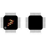
| 产品图片 |
|
| rohs | 符合RoHS无铅 / 符合限制有害物质指令(RoHS)规范要求 |
| 产品系列 | 嵌入式处理器和控制器,微控制器 - MCU,ARM微控制器 - MCU,Freescale Semiconductor MKL05Z32VLF4Kinetis KL0 |
| 数据手册 | |
| 产品型号 | MKL05Z32VLF4 |
| PCN其它 | http://cache.freescale.com/files/shared/doc/pcn/PCN15938.htm |
| PCN设计/规格 | http://cache.freescale.com/files/shared/doc/pcn/PCN15823.htmhttp://cache.freescale.com/files/shared/doc/pcn/PCN16204.htm |
| RAM容量 | 4K x 8 |
| 产品种类 | ARM微控制器 - MCU |
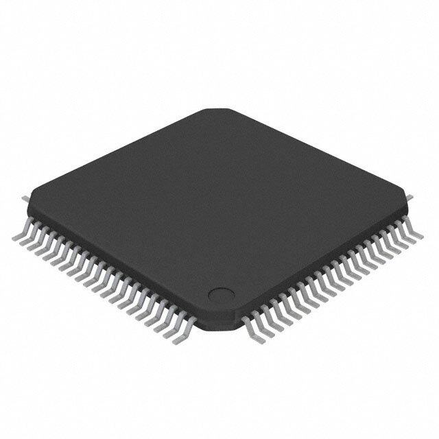
| 供应商器件封装 | 48-LQFP(7x7) |
| 包装 | 托盘 |
| 单位重量 | 178.250 mg |
| 商标 | Freescale Semiconductor |
| 商标名 | Kinetis |
| 处理器系列 | Kinetis L |
| 外设 | 欠压检测/复位,DMA,LVD,POR,PWM,WDT |
| 安装风格 | SMD/SMT |
| 封装 | Tray |
| 封装/外壳 | 48-LQFP |
| 封装/箱体 | LQFP-48 |
| 工作温度 | -40°C ~ 105°C |
| 工作电源电压 | 1.71 V to 3.6 V |
| 工厂包装数量 | 250 |
| 振荡器类型 | 内部 |
| 数据RAM大小 | 4 kB |
| 数据总线宽度 | 32 bit |
| 数据转换器 | A/D 14x12b,D/A 1x12b |
| 最大工作温度 | + 105 C |
| 最大时钟频率 | 48 MHz |
| 最小工作温度 | - 40 C |
| 标准包装 | 250 |
| 核心 | ARM Cortex M0 |
| 核心处理器 | ARM® Cortex™-M0+ |
| 核心尺寸 | 32-位 |
| 片上ADC | Yes |
| 电压-电源(Vcc/Vdd) | 1.71 V ~ 3.6 V |
| 程序存储器大小 | 32 kB |
| 程序存储器类型 | 闪存 |
| 程序存储容量 | 32KB(32K x 8) |
| 系列 | KL0 |
| 连接性 | I²C, SPI, UART/USART |
| 速度 | 48MHz |


PDF Datasheet 数据手册内容提取
Freescale Semiconductor, Inc. KL05P48M48SF1 Data Sheet: Technical Data Rev 4 03/2014 Kinetis KL05 32 KB Flash MKL05ZxxVFK4 48 MHz Cortex-M0+ Based Microcontroller MKL05ZxxVLC4 MKL05ZxxVFM4 Designed with efficiency in mind. Features a size efficient, small MKL05ZxxVLF4 package, energy efficient ARM Cortex-M0+ 32-bit performance. Shares the comprehensive enablement and scalability of the Kinetis family. This product offers: • Run power consumption down to 45 μA/MHz in very low 24-pin QFN (FK) 32-pin QFN (FM) power run mode 4 x 4 x 1 Pitch 0.5 mm 5 x 5 x 1 Pitch 0.5 mm • Static power consumption down to 2 μA with full state retention and 4 μs wakeup • Ultra-efficient Cortex-M0+ processor running up to 48MHz with industry leading throughput • Memory option is up to 32 KB Flash and 4 KB RAM 32-pin LQFP (LC) 48-pin LQFP (LF) • Energy-saving architecture is optimized for low power with 7 x 7 x 1.4 Pitch 0.8 7 x 7 x 1.4 Pitch 0.5 90 nm TFS technology, clock and power gating techniques, mm mm and zero wait state flash memory controller Performance Human-machine interface • 48 MHz ARM® Cortex®-M0+ core • Low-power hardware touch sensor interface (TSI) • Up to 41 general-purpose input/output (GPIO) Memories and memory interfaces • Up to 32 KB program flash memory Communication interfaces • Up to 4 KB SRAM • One 8-bit SPI module • One low power UART module System peripherals • One I2C module • Nine low-power modes to provide power optimization based on application requirements Analog Modules • COP Software watchdog • 12-bit SAR ADC • 4-channel DMA controller, supporting up to 63 request • 12-bit DAC sources • Analog comparator (CMP) containing a 6-bit DAC • Low-leakage wakeup unit and programmable reference input • SWD debug interface and Micro Trace Buffer • Bit Manipulation Engine Timers • Six channel Timer/PWM (TPM) Clocks • One 2-channel Timer/PWM module • 32 kHz to 40 kHz or 3 MHz to 32 MHz crystal oscillator • Periodic interrupt timers • Multi-purpose clock source • 16-bit low-power timer (LPTMR) • 1 kHz LPO clock • Real time clock Operating Characteristics Security and integrity modules • Voltage range: 1.71 to 3.6 V • 80-bit unique identification number per chip • Flash write voltage range: 1.71 to 3.6 V • Temperature range (ambient): -40 to 105°C Freescale reserves the right to change the detail specifications as may be required to permit improvements in the design of its products. © 2012–2014 Freescale Semiconductor, Inc. All rights reserved.
Ordering Information Part Number Memory Maximum number of I\O's Flash (KB) SRAM (KB) MKL05Z8VFK4 8 1 22 MKL05Z16VFK4 16 2 22 MKL05Z32VFK4 32 4 22 MKL05Z8VLC4 8 1 28 MKL05Z16VLC4 16 2 28 MKL05Z32VLC4 32 4 28 MKL05Z8VFM4 8 1 28 MKL05Z16VFM4 16 2 28 MKL05Z32VFM4 32 4 28 MKL05Z16VLF4 16 2 41 MKL05Z32VLF4 32 4 41 Related Resources Type Description Selector Guide The Freescale Solution Advisor is a web-based tool that features interactive application wizards and a dynamic product selector. Product Brief The Product Brief contains concise overview/summary information to enable quick evaluation of a device for design suitability. Reference Manual The Reference Manual contains a comprehensive description of the structure and function (operation) of a device. Data Sheet The Data Sheet includes electrical characteristics and signal connections. Chip Errata The chip mask set Errata provides additional or corrective information for a particular device mask set. Package drawing Package dimensions are provided in package drawings. 2 Kinetis KL05 32 KB Flash, Rev4 03/2014. Freescale Semiconductor, Inc.
Table of Contents 1 Ratings..................................................................................4 3.6.2 CMP and 6-bit DAC electrical specifications......28 1.1 Thermal handling ratings...............................................4 3.6.3 12-bit DAC electrical characteristics..................30 1.2 Moisture handling ratings...............................................4 3.7 Timers............................................................................33 1.3 ESD handling ratings.....................................................4 3.8 Communication interfaces.............................................33 1.4 Voltage and current operating ratings............................4 3.8.1 SPI switching specifications...............................33 2 General.................................................................................5 3.8.2 Inter-Integrated Circuit Interface (I2C) timing.....38 2.1 AC electrical characteristics...........................................5 3.8.3 UART.................................................................39 2.2 Nonswitching electrical specifications............................5 3.9 Human-machine interfaces (HMI)..................................39 2.2.1 Voltage and current operating requirements......5 3.9.1 TSI electrical specifications................................39 2.2.2 LVD and POR operating requirements..............6 4 Dimensions...........................................................................40 2.2.3 Voltage and current operating behaviors...........7 4.1 Obtaining package dimensions......................................40 2.2.4 Power mode transition operating behaviors.......8 5 Pinout....................................................................................40 2.2.5 Power consumption operating behaviors...........9 5.1 KL05 signal multiplexing and pin assignments..............40 2.2.6 EMC performance..............................................15 5.2 KL05 pinouts..................................................................42 2.2.7 Capacitance attributes.......................................16 6 Ordering parts.......................................................................46 2.3 Switching specifications.................................................16 6.1 Determining valid orderable parts..................................46 2.3.1 Device clock specifications................................16 7 Part identification...................................................................46 2.3.2 General switching specifications........................17 7.1 Description.....................................................................46 2.4 Thermal specifications...................................................17 7.2 Format...........................................................................47 2.4.1 Thermal operating requirements........................17 7.3 Fields.............................................................................47 2.4.2 Thermal attributes..............................................17 7.4 Example.........................................................................47 3 Peripheral operating requirements and behaviors................18 8 Terminology and guidelines..................................................48 3.1 Core modules................................................................18 8.1 Definition: Operating requirement..................................48 3.1.1 SWD electricals .................................................18 8.2 Definition: Operating behavior.......................................48 3.2 System modules............................................................19 8.3 Definition: Attribute........................................................48 3.3 Clock modules...............................................................20 8.4 Definition: Rating...........................................................49 3.3.1 MCG specifications............................................20 8.5 Result of exceeding a rating..........................................49 3.3.2 Oscillator electrical specifications......................21 8.6 Relationship between ratings and operating 3.4 Memories and memory interfaces.................................23 requirements..................................................................49 3.4.1 Flash electrical specifications............................23 8.7 Guidelines for ratings and operating requirements........50 3.5 Security and integrity modules.......................................25 8.8 Definition: Typical value.................................................50 3.6 Analog............................................................................25 8.9 Typical value conditions.................................................51 3.6.1 ADC electrical specifications..............................25 9 Revision history.....................................................................52 Kinetis KL05 32 KB Flash, Rev4 03/2014. 3 Freescale Semiconductor, Inc.
Ratings 1 Ratings 1.1 Thermal handling ratings Table 1. Thermal handling ratings Symbol Description Min. Max. Unit Notes T Storage temperature –55 150 °C 1 STG T Solder temperature, lead-free — 260 °C 2 SDR 1. Determined according to JEDEC Standard JESD22-A103, High Temperature Storage Life. 2. Determined according to IPC/JEDEC Standard J-STD-020, Moisture/Reflow Sensitivity Classification for Nonhermetic Solid State Surface Mount Devices. 1.2 Moisture handling ratings Table 2. Moisture handling ratings Symbol Description Min. Max. Unit Notes MSL Moisture sensitivity level — 3 — 1 1. Determined according to IPC/JEDEC Standard J-STD-020, Moisture/Reflow Sensitivity Classification for Nonhermetic Solid State Surface Mount Devices. 1.3 ESD handling ratings Table 3. ESD handling ratings Symbol Description Min. Max. Unit Notes V Electrostatic discharge voltage, human body model –2000 +2000 V 1 HBM V Electrostatic discharge voltage, charged-device –500 +500 V 2 CDM model I Latch-up current at ambient temperature of 105 °C –100 +100 mA 3 LAT 1. Determined according to JEDEC Standard JESD22-A114, Electrostatic Discharge (ESD) Sensitivity Testing Human Body Model (HBM). 2. Determined according to JEDEC Standard JESD22-C101, Field-Induced Charged-Device Model Test Method for Electrostatic-Discharge-Withstand Thresholds of Microelectronic Components. 3. Determined according to JEDEC Standard JESD78, IC Latch-Up Test. 4 Kinetis KL05 32 KB Flash, Rev4 03/2014. Freescale Semiconductor, Inc.
General 1.4 Voltage and current operating ratings Table 4. Voltage and current operating ratings Symbol Description Min. Max. Unit V Digital supply voltage –0.3 3.8 V DD I Digital supply current — 120 mA DD V IO pin input voltage –0.3 V + 0.3 V IO DD I Instantaneous maximum current single pin limit (applies to –25 25 mA D all port pins) V Analog supply voltage V – 0.3 V + 0.3 V DDA DD DD 2 General 2.1 AC electrical characteristics Unless otherwise specified, propagation delays are measured from the 50% to the 50% point, and rise and fall times are measured at the 20% and 80% points, as shown in the following figure. Figure 1. Input signal measurement reference All digital I/O switching characteristics, unless otherwise specified, assume the output pins have the following characteristics. • C =30 pF loads L • Slew rate disabled • Normal drive strength 2.2 Nonswitching electrical specifications Kinetis KL05 32 KB Flash, Rev4 03/2014. 5 Freescale Semiconductor, Inc.
General 2.2.1 Voltage and current operating requirements Table 5. Voltage and current operating requirements Symbol Description Min. Max. Unit Notes V Supply voltage 1.71 3.6 V DD V Analog supply voltage 1.71 3.6 V — DDA V – V V -to-V differential voltage –0.1 0.1 V — DD DDA DD DDA V – V V -to-V differential voltage –0.1 0.1 V — SS SSA SS SSA V Input high voltage — IH • 2.7 V ≤ V ≤ 3.6 V 0.7 × V — V DD DD • 1.7 V ≤ V ≤ 2.7 V 0.75 × V — V DD DD V Input low voltage — IL • 2.7 V ≤ V ≤ 3.6 V — 0.35 × V V DD DD • 1.7 V ≤ V ≤ 2.7 V — 0.3 × V V DD DD V Input hysteresis 0.06 × V — V — HYS DD I IO pin negative DC injection current—single pin 1 ICIO –3 — mA • V < V –0.3V (negative current injection) IN SS • V < V –0.3V (positive current injection) — +3 IN SS I Contiguous pin DC injection current —regional limit, — ICcont includes sum of negative injection currents or sum of positive injection currents of 16 contiguous pins –25 — mA • Negative current injection — +25 • Positive current injection V Open drain pullup voltage level V V V 2 ODPU DD DD V V voltage required to retain RAM 1.2 — V — RAM DD 1. All IO pins are internally clamped to V and V through ESD protection diodes. If V is greater than V SS DD IN IO_MIN (=V -0.3V) and V is less than V (=V +0.3V) is observed, then there is no need to provide current limiting SS IN IO_MAX DD resistors at the pads. If these limits cannot be observed then a current limiting resistor is required. The negative DC injection current limiting resistor is calculated as R=(V -V )/|I |. The positive injection current limiting resistor is IO_MIN IN ICIO calculated as R=(V -V )/|I |. Select the larger of these two calculated resistances. IN IO_MAX ICIO 2. Open drain outputs must be pulled to V . DD 2.2.2 LVD and POR operating requirements Table 6. V supply LVD and POR operating requirements DD Symbol Description Min. Typ. Max. Unit Notes V Falling V POR detect voltage 0.8 1.1 1.5 V — POR DD V Falling low-voltage detect threshold — high 2.48 2.56 2.64 V — LVDH range (LVDV = 01) Low-voltage warning thresholds — high range 1 Table continues on the next page... 6 Kinetis KL05 32 KB Flash, Rev4 03/2014. Freescale Semiconductor, Inc.
General Table 6. V supply LVD and POR operating requirements (continued) DD Symbol Description Min. Typ. Max. Unit Notes V • Level 1 falling (LVWV = 00) 2.62 2.70 2.78 V LVW1H V • Level 2 falling (LVWV = 01) 2.72 2.80 2.88 V LVW2H V • Level 3 falling (LVWV = 10) 2.82 2.90 2.98 V LVW3H V • Level 4 falling (LVWV = 11) 2.92 3.00 3.08 V LVW4H V Low-voltage inhibit reset/recover hysteresis — — ±60 — mV — HYSH high range V Falling low-voltage detect threshold — low 1.54 1.60 1.66 V — LVDL range (LVDV=00) Low-voltage warning thresholds — low range 1 V • Level 1 falling (LVWV = 00) LVW1L 1.74 1.80 1.86 V V • Level 2 falling (LVWV = 01) LVW2L 1.84 1.90 1.96 V V • Level 3 falling (LVWV = 10) LVW3L 1.94 2.00 2.06 V V • Level 4 falling (LVWV = 11) LVW4L 2.04 2.10 2.16 V V Low-voltage inhibit reset/recover hysteresis — — ±40 — mV — HYSL low range V Bandgap voltage reference 0.97 1.00 1.03 V — BG t Internal low power oscillator period — factory 900 1000 1100 μs — LPO trimmed 1. Rising thresholds are falling threshold + hysteresis voltage 2.2.3 Voltage and current operating behaviors Table 7. Voltage and current operating behaviors Symbol Description Min. Max. Unit Notes V Output high voltage — Normal drive pad (except 1, 2 OH RESET) V – 0.5 — V • 2.7 V ≤ V ≤ 3.6 V, I = –5 mA DD DD OH V – 0.5 — V • 1.71 V ≤ V ≤ 2.7 V, I = –1.5 mA DD DD OH V Output high voltage — High drive pad (except 1, 2 OH RESET_b) V – 0.5 — V • 2.7 V ≤ V ≤ 3.6 V, I = –18 mA DD DD OH V – 0.5 — V • 1.71 V ≤ V ≤ 2.7 V, I = –6 mA DD DD OH I Output high current total for all ports — 100 mA OHT V Output low voltage — Normal drive pad 1 OL • 2.7 V ≤ V ≤ 3.6 V, I = 5 mA DD OL — 0.5 V • 1.71 V ≤ V ≤ 2.7 V, I = 1.5 mA DD OL — 0.5 V Table continues on the next page... Kinetis KL05 32 KB Flash, Rev4 03/2014. 7 Freescale Semiconductor, Inc.
General Table 7. Voltage and current operating behaviors (continued) Symbol Description Min. Max. Unit Notes V Output low voltage — High drive pad 1 OL • 2.7 V ≤ V ≤ 3.6 V, I = 18 mA DD OL — 0.5 V • 1.71 V ≤ V ≤ 2.7 V, I = 6 mA DD OL — 0.5 V I Output low current total for all ports — 100 mA OLT I Input leakage current (per pin) for full temperature — 1 μA 3 IN range I Input leakage current (per pin) at 25 °C — 0.025 μA 3 IN I Input leakage current (total all pins) for full — 41 μA 3 IN temperature range I Hi-Z (off-state) leakage current (per pin) — 1 μA OZ R Internal pullup resistors 20 50 kΩ 4 PU 1. PTA12, PTA13, PTB0 and PTB1 I/O have both high drive and normal drive capability selected by the associated PTx_PCRn[DSE] control bit. All other GPIOs are normal drive only. 2. The reset pin only contains an active pull down device when configured as the RESET signal or as a GPIO. When configured as a GPIO output, it acts as a pseudo open drain output. 3. Measured at V = 3.6 V DD 4. Measured at V supply voltage = V min and Vinput = V DD DD SS 2.2.4 Power mode transition operating behaviors All specifications except t and VLLSx→RUN recovery times in the following table POR assume this clock configuration: • CPU and system clocks = 48 MHz • Bus and flash clock = 24 MHz • FEI clock mode POR and VLLSx→RUN recovery use FEI clock mode at the default CPU and system frequency of 21 MHz, and a bus and flash clock frequency of 10.5 MHz. Table 8. Power mode transition operating behaviors Symbol Description Min. Typ. Max. Unit t After a POR event, amount of time from the — — 300 μs 1 POR point V reaches 1.8 V to execution of the first DD instruction across the operating temperature range of the chip. • VLLS0 → RUN — 95 115 μs • VLLS1 → RUN Table continues on the next page... 8 Kinetis KL05 32 KB Flash, Rev4 03/2014. Freescale Semiconductor, Inc.
General Table 8. Power mode transition operating behaviors (continued) Symbol Description Min. Typ. Max. Unit — 93 115 μs • VLLS3 → RUN — 42 53 μs • LLS → RUN — 4 4.6 μs • VLPS → RUN — 4 4.4 μs • STOP → RUN — 4 4.4 μs 1. Normal boot (FTFA_FOPT[LPBOOT]=11). 2.2.5 Power consumption operating behaviors The maximum values stated in the following table represent characterized results equivalent to the mean plus three times the standard deviation (mean + 3 sigma). Table 9. Power consumption operating behaviors Symbol Description Min. Typ. Max.1 Unit Notes I Analog supply current — — See note mA 2 DDA I Run mode current in compute operation - 48 3 DD_RUNCO MHz core / 24 MHz flash / bus clock disabled, code of while(1) loop executing from flash — 4.0 4.3 mA • at 3.0 V I Run mode current - 48 MHz core / 24 MHz bus 3 DD_RUN and flash, all peripheral clocks disabled, code executing from flash — 4.9 5.3 mA • at 3.0 V I Run mode current - 48 MHz core / 24 MHz bus 3, 4 DD_RUN and flash, all peripheral clocks enabled, code executing from flash mA • at 3.0 V — 5.7 5.8 • at 25 °C — 6.0 6.2 • at 125 °C I Wait mode current - core disabled / 48 MHz 3 DD_WAIT system / 24 MHz bus / flash disabled (flash doze enabled), all peripheral clocks disabled — 2.7 2.9 mA • at 3.0 V Table continues on the next page... Kinetis KL05 32 KB Flash, Rev4 03/2014. 9 Freescale Semiconductor, Inc.
General Table 9. Power consumption operating behaviors (continued) Symbol Description Min. Typ. Max.1 Unit Notes I Wait mode current - core disabled / 24 MHz 3 DD_WAIT system / 24 MHz bus / flash disabled (flash doze enabled), all peripheral clocks disabled — 2.2 2.3 mA • at 3.0 V I Stop mode current with partial stop 2 clocking 3 DD_PSTOP2 option - core and system disabled / 10.5 MHz bus / flash disabled (flash doze enabled) — 1.5 1.7 mA • at 3.0 V I Very-low-power run mode current in compute 5 DD_VLPRCO operation - 4 MHz core / 0.8 MHz flash / bus clock disabled, code executing from flash — 182 253 μA • at 3.0 V I Very low power run mode current - 4 MHz 5 DD_VLPR core / 0.8 MHz bus and flash, all peripheral clocks disabled, code executing from flash — 213 284 μA • at 3.0 V I Very low power run mode current - 4 MHz 4, 5 DD_VLPR core / 0.8 MHz bus and flash, all peripheral clocks enabled, code executing from flash — 243 313 μA • at 3.0 V I Very low power wait mode current - core 5 DD_VLPW disabled / 4 MHz system / 0.8 MHz bus / flash — 111 170 μA disabled (flash doze enabled), all peripheral clocks disabled • at 3.0 V I Stop mode current DD_STOP • at 3.0 V μA — 257 277 • at 25 °C — 265 285 • at 50 °C — 278 303 • at 70 °C — 295 326 • at 85 °C — 353 412 • at 105 °C I Very-low-power stop mode current DD_VLPS • at 3.0 V — 2.25 5.76 μA • at 25 °C — 4.08 8.27 • at 50 °C — 8.10 14.52 • at 70 °C — 14.18 23.78 • at 85 °C — 37.07 58.58 • at 105 °C I Low-leakage stop mode current DD_LLS • at 3.0 V Table continues on the next page... 10 Kinetis KL05 32 KB Flash, Rev4 03/2014. Freescale Semiconductor, Inc.
General Table 9. Power consumption operating behaviors (continued) Symbol Description Min. Typ. Max.1 Unit Notes • at 25 °C — 1.72 2.01 μA • at 50 °C — 2.52 3.18 • at 70 °C — 4.32 5.94 • at 85 °C — 7.18 10.00 • at 105 °C — 18.67 25.65 I Very-low-leakage stop mode 3 current DD_VLLS3 • at 3.0 V μA — 1.16 1.36 • at 25 °C — 1.78 2.27 • at 50 °C — 3.23 4.38 • at 70 °C — 5.57 7.53 • at 85 °C — 14.80 19.74 • at 105 °C I Very-low-leakage stop mode 1 current DD_VLLS1 • at 3.0 V — 0.64 0.81 μA • at 25°C — 1.14 1.50 • at 50°C — 2.35 3.20 • at 70°C — 4.37 5.80 • at 85°C — 12.40 16.13 • at 105°C I Very-low-leakage stop mode 0 current DD_VLLS0 (SMC_STOPCTRL[PORPO] = 0) • at 3.0 V — 0.38 0.54 μA • at 25 °C — 0.88 1.23 • at 50 °C — 2.10 2.95 • at 70 °C — 4.14 5.59 • at 85 °C — 12.00 15.73 • at 105 °C I Very-low-leakage stop mode 0 current 6 DD_VLLS0 (SMC_STOPCTRL[PORPO] = 1) • at 3.0 V — 0.30 0.45 μA • at 25 °C — 0.79 1.12 • at 50 °C — 2.01 2.82 • at 70 °C — 4.05 5.45 • at 85 °C — 11.96 15.63 • at 105 °C 1. Data based on characterization results. Kinetis KL05 32 KB Flash, Rev4 03/2014. 11 Freescale Semiconductor, Inc.
General 2. The analog supply current is the sum of the active or disabled current for each of the analog modules on the device. See each module's specification for its supply current. 3. MCG configured for FEI mode. 4. Incremental current consumption from peripheral activity is not included. 5. MCG configured for BLPI mode. 6. No brownout Table 10. Low power mode peripheral adders — typical value Symbol Description Temperature (°C) Unit -40 25 50 70 85 105 I 4 MHz internal reference clock (IRC) 56 56 56 56 56 56 µA IREFSTEN4MHz adder. Measured by entering STOP or VLPS mode with 4 MHz IRC enabled. I 32 kHz internal reference clock (IRC) 52 52 52 52 52 52 µA IREFSTEN32KHz adder. Measured by entering STOP mode with the 32 kHz IRC enabled. I External 4 MHz crystal clock adder. 206 228 237 245 251 258 uA EREFSTEN4MHz Measured by entering STOP or VLPS mode with the crystal enabled. I External 32 kHz crystal clock adder by EREFSTEN32KHz means of the OSC0_CR[EREFSTEN 440 490 540 560 570 580 and EREFSTEN] bits. Measured by entering all modes with the crystal 440 490 540 560 570 580 nA enabled. 490 490 540 560 570 680 • VLLS1 • VLLS3 510 560 560 560 610 680 • LLS 510 560 560 560 610 680 • VLPS • STOP I CMP peripheral adder measured by 22 22 22 22 22 22 µA CMP placing the device in VLLS1 mode with CMP enabled using the 6-bit DAC and a single external input for compare. Includes 6-bit DAC power consumption. I RTC peripheral adder measured by 432 357 388 475 532 810 nA RTC placing the device in VLLS1 mode with external 32 kHz crystal enabled by means of the RTC_CR[OSCE] bit and the RTC ALARM set for 1 minute. Includes ERCLK32K (32 kHz external crystal) power consumption. I UART peripheral adder measured by UART placing the device in STOP or VLPS mode with selected clock source waiting 66 66 66 66 66 66 µA for RX data at 115200 baud rate. Includes selected clock source power 214 237 246 254 260 268 consumption. • MCGIRCLK (4 MHz internal reference clock) • OSCERCLK (4 MHz external crystal) Table continues on the next page... 12 Kinetis KL05 32 KB Flash, Rev4 03/2014. Freescale Semiconductor, Inc.
General Table 10. Low power mode peripheral adders — typical value (continued) Symbol Description Temperature (°C) Unit -40 25 50 70 85 105 I TPM peripheral adder measured by TPM placing the device in STOP or VLPS mode with selected clock source µA configured for output compare 86 86 86 86 86 86 generating 100 Hz clock signal. No load is placed on the I/O generating the 235 256 265 274 280 287 clock signal. Includes selected clock source and I/O switching currents. • MCGIRCLK (4 MHz internal reference clock) • OSCERCLK (4 MHz external crystal) I Bandgap adder when BGEN bit is set 45 45 45 45 45 45 µA BG and device is placed in VLPx, LLS, or VLLSx mode. I ADC peripheral adder combining the 366 366 366 366 366 366 µA ADC measured values at V and V by DD DDA placing the device in STOP or VLPS mode. ADC is configured for low power mode using the internal clock and continuous conversions. 2.2.5.1 Diagram: Typical IDD_RUN operating behavior The following data was measured under these conditions: • MCG in FBE for run mode, and BLPE for VLPR mode • No GPIOs toggled • Code execution from flash with cache enabled • For the ALLOFF curve, all peripheral clocks are disabled except FTFA Kinetis KL05 32 KB Flash, Rev4 03/2014. 13 Freescale Semiconductor, Inc.
General Run Mode Current VS Core Frequency Temperature = 25, VDD = 3, CACHE = Enable, Code Residence = Flash, Clocking Mode = FBE 7.00E-03 6.00E-03 5.00E-03 )A ( D D V n 4.00E-03 o n All Peripheral CLK Gates o itp All Off m u 3.00E-03 All On s n o C tn erru 2.00E-03 C 1.00E-03 000.00E+00 CLK Ratio '1-1 '1-1 '1-1 '1-1 '1-1 '1-1 '1-1 '1-2 Flash-Core 1 2 3 4 6 12 24 48 Core Freq (MHz) Figure 2. Run mode supply current vs. core frequency 14 Kinetis KL05 32 KB Flash, Rev4 03/2014. Freescale Semiconductor, Inc.
General VLPR Mode Current VS Core Frequency Temperature = 25, VDD = 3, CACHE = Enable, Code Residence = Flash, Clocking Mode = BLPE 350.00E-06 300.00E-06 250.00E-06 )A ( DD 200.00E-06 V All Peripheral CLK Gates n o n o All Off itp 150.00E-06 All On m u s n o C tn 100.00E-06 e rru C 50.00E-06 000.00E+00 CLK Ratio '1-1 '1-2 '1-2 '1-4 Flash-Core 1 2 4 Core Freq (MHz) Figure 3. VLPR mode current vs. core frequency 2.2.6 EMC performance Electromagnetic compatibility (EMC) performance is highly dependent on the environment in which the MCU resides. Board design and layout, circuit topology choices, location and characteristics of external components as well as MCU software operation play a significant role in EMC performance. The system designer must consult the following Freescale applications notes, available on freescale.com for advice and guidance specifically targeted at optimizing EMC performance. • AN2321: Designing for Board Level Electromagnetic Compatibility • AN1050: Designing for Electromagnetic Compatibility (EMC) with HCMOS Microcontrollers • AN1263: Designing for Electromagnetic Compatibility with Single-Chip Microcontrollers Kinetis KL05 32 KB Flash, Rev4 03/2014. 15 Freescale Semiconductor, Inc.
General • AN2764: Improving the Transient Immunity Performance of Microcontroller- Based Applications • AN1259: System Design and Layout Techniques for Noise Reduction in MCU- Based Systems 2.2.7 Capacitance attributes Table 11. Capacitance attributes Symbol Description Min. Max. Unit C Input capacitance — 7 pF IN 2.3 Switching specifications 2.3.1 Device clock specifications Table 12. Device clock specifications Symbol Description Min. Max. Unit Normal run mode f System and core clock — 48 MHz SYS f Bus clock — 24 MHz BUS f Flash clock — 24 MHz FLASH f LPTMR clock — 24 MHz LPTMR VLPR and VLPS modes1 f System and core clock — 4 MHz SYS f Bus clock — 1 MHz BUS f Flash clock — 1 MHz FLASH f LPTMR clock2 — 24 MHz LPTMR f External reference clock — 16 MHz ERCLK f LPTMR external reference clock — 16 MHz LPTMR_ERCLK f Oscillator crystal or resonator frequency — high frequency — 16 MHz osc_hi_2 mode (high range) (MCG_C2[RANGE]=1x) f TPM asynchronous clock — 8 MHz TPM f UART0 asynchronous clock — 8 MHz UART0 1. The frequency limitations in VLPR and VLPS modes here override any frequency specification listed in the timing specification for any other module. These same frequency limits apply to VLPS, whether VLPS was entered from RUN or from VLPR. 2. The LPTMR can be clocked at this speed in VLPR or VLPS only when the source is an external pin. 16 Kinetis KL05 32 KB Flash, Rev4 03/2014. Freescale Semiconductor, Inc.
General 2.3.2 General switching specifications These general-purpose specifications apply to all signals configured for GPIO and UART signals. Table 13. General switching specifications Description Min. Max. Unit Notes GPIO pin interrupt pulse width (digital glitch filter disabled) 1.5 — Bus clock 1 — Synchronous path cycles External RESET and NMI pin interrupt pulse width — 100 — ns 2 Asynchronous path GPIO pin interrupt pulse width — Asynchronous path 16 — ns 2 Port rise and fall time — 36 ns 3 1. The greater synchronous and asynchronous timing must be met. 2. This is the shortest pulse that is guaranteed to be recognized. 3. 75 pF load 2.4 Thermal specifications 2.4.1 Thermal operating requirements Table 14. Thermal operating requirements Symbol Description Min. Max. Unit T Die junction temperature –40 125 °C J T Ambient temperature –40 105 °C A 2.4.2 Thermal attributes Table 15. Thermal attributes Board type Symbol Description 48 32 32 QFN 24 QFN Unit Notes LQFP LQFP Single-layer (1S) R Thermal resistance, junction 82 88 97 110 °C/W 1 θJA to ambient (natural convection) Four-layer (2s2p) R Thermal resistance, junction 58 59 34 42 °C/W θJA to ambient (natural convection) Table continues on the next page... Kinetis KL05 32 KB Flash, Rev4 03/2014. 17 Freescale Semiconductor, Inc.
Peripheral operating requirements and behaviors Table 15. Thermal attributes (continued) Board type Symbol Description 48 32 32 QFN 24 QFN Unit Notes LQFP LQFP Single-layer (1S) R Thermal resistance, junction 70 74 81 92 °C/W θJMA to ambient (200 ft./min. air speed) Four-layer (2s2p) R Thermal resistance, junction 52 52 28 36 °C/W θJMA to ambient (200 ft./min. air speed) — R Thermal resistance, junction 36 35 13 18 °C/W 2 θJB to board — R Thermal resistance, junction 27 26 2.3 3.7 °C/W 3 θJC to case — Ψ Thermal characterization 8 8 8 10 °C/W 4 JT parameter, junction to package top outside center (natural convection) 1. Determined according to JEDEC Standard JESD51-2, Integrated Circuits Thermal Test Method Environmental Conditions—Natural Convection (Still Air), or EIA/JEDEC Standard JESD51-6, Integrated Circuit Thermal Test Method Environmental Conditions—Forced Convection (Moving Air). 2. Determined according to JEDEC Standard JESD51-8, Integrated Circuit Thermal Test Method Environmental Conditions—Junction-to-Board. 3. Determined according to Method 1012.1 of MIL-STD 883, Test Method Standard, Microcircuits, with the cold plate temperature used for the case temperature. The value includes the thermal resistance of the interface material between the top of the package and the cold plate. 4. Determined according to JEDEC Standard JESD51-2, Integrated Circuits Thermal Test Method Environmental Conditions—Natural Convection (Still Air). 3 Peripheral operating requirements and behaviors 3.1 Core modules 3.1.1 SWD electricals Table 16. SWD full voltage range electricals Symbol Description Min. Max. Unit Operating voltage 1.71 3.6 V J1 SWD_CLK frequency of operation • Serial wire debug 0 25 MHz J2 SWD_CLK cycle period 1/J1 — ns J3 SWD_CLK clock pulse width Table continues on the next page... 18 Kinetis KL05 32 KB Flash, Rev4 03/2014. Freescale Semiconductor, Inc.
Peripheral operating requirements and behaviors Table 16. SWD full voltage range electricals (continued) Symbol Description Min. Max. Unit • Serial wire debug 20 — ns J4 SWD_CLK rise and fall times — 3 ns J9 SWD_DIO input data setup time to SWD_CLK rise 10 — ns J10 SWD_DIO input data hold time after SWD_CLK rise 0 — ns J11 SWD_CLK high to SWD_DIO data valid — 32 ns J12 SWD_CLK high to SWD_DIO high-Z 5 — ns J2 J3 J3 SWD_CLK (input) J4 J4 Figure 4. Serial wire clock input timing SWD_CLK J9 J10 SWD_DIO Input data valid J11 SWD_DIO Output data valid J12 SWD_DIO J11 SWD_DIO Output data valid Figure 5. Serial wire data timing Kinetis KL05 32 KB Flash, Rev4 03/2014. 19 Freescale Semiconductor, Inc.
Peripheral operating requirements and behaviors 3.2 System modules There are no specifications necessary for the device's system modules. 3.3 Clock modules 3.3.1 MCG specifications Table 17. MCG specifications Symbol Description Min. Typ. Max. Unit Notes f Internal reference frequency (slow clock) — — 32.768 — kHz ints_ft factory trimmed at nominal V and 25 °C DD f Internal reference frequency (slow clock) — 31.25 — 39.0625 kHz ints_t user trimmed Δ Resolution of trimmed average DCO output — ± 0.3 ± 0.6 %f 1 fdco_res_t dco frequency at fixed voltage and temperature — using C3[SCTRIM] and C4[SCFTRIM] Δf Total deviation of trimmed average DCO output — +0.5/-0.7 ± 3 %f 1, 2 dco_t dco frequency over voltage and temperature Δf Total deviation of trimmed average DCO output — ± 0.4 ± 1.5 %f 1, 2 dco_t dco frequency over fixed voltage and temperature range of 0–70 °C f Internal reference frequency (fast clock) — — 4 — MHz intf_ft factory trimmed at nominal V and 25 °C DD Δf Frequency deviation of internal reference clock — +1/-2 ± 3 %f 2 intf_ft intf_ft (fast clock) over temperature and voltage — factory trimmed at nominal V and 25 °C DD f Internal reference frequency (fast clock) — user 3 — 5 MHz intf_t trimmed at nominal V and 25 °C DD f Loss of external clock minimum frequency — (3/5) x — — kHz loc_low RANGE = 00 f ints_t f Loss of external clock minimum frequency — (16/5) x — — kHz loc_high RANGE = 01, 10, or 11 f ints_t FLL f FLL reference frequency range 31.25 — 39.0625 kHz fll_ref f DCO output Low range (DRS = 00) 20 20.97 25 MHz 3, 4 dco frequency range 640 × f fll_ref Mid range (DRS = 01) 40 41.94 48 MHz 1280 × f fll_ref f DCO output Low range (DRS = 00) — 23.99 — MHz 5, 6 dco_t_DMX3 frequency 2 732 × f fll_ref Mid range (DRS = 01) — 47.97 — MHz Table continues on the next page... 20 Kinetis KL05 32 KB Flash, Rev4 03/2014. Freescale Semiconductor, Inc.
Peripheral operating requirements and behaviors Table 17. MCG specifications (continued) Symbol Description Min. Typ. Max. Unit Notes 1464 × f fll_ref J FLL period jitter — 180 — ps 7 cyc_fll • f = 48 MHz VCO t FLL target frequency acquisition time — — 1 ms 8 fll_acquire 1. This parameter is measured with the internal reference (slow clock) being used as a reference to the FLL (FEI clock mode). 2. The deviation is relative to the factory trimmed frequency at nominal V and 25 °C, f . DD ints_ft 3. These typical values listed are with the slow internal reference clock (FEI) using factory trim and DMX32 = 0. 4. The resulting system clock frequencies must not exceed their maximum specified values. The DCO frequency deviation (Δf ) over voltage and temperature must be considered. dco_t 5. These typical values listed are with the slow internal reference clock (FEI) using factory trim and DMX32 = 1. 6. The resulting clock frequency must not exceed the maximum specified clock frequency of the device. 7. This specification is based on standard deviation (RMS) of period or frequency. 8. This specification applies to any time the FLL reference source or reference divider is changed, trim value is changed, DMX32 bit is changed, DRS bits are changed, or changing from FLL disabled (BLPE, BLPI) to FLL enabled (FEI, FEE, FBE, FBI). If a crystal/resonator is being used as the reference, this specification assumes it is already running. 3.3.2 Oscillator electrical specifications 3.3.2.1 Oscillator DC electrical specifications Table 18. Oscillator DC electrical specifications Symbol Description Min. Typ. Max. Unit Notes V Supply voltage 1.71 — 3.6 V DD I Supply current — low-power mode (HGO=0) 1 DDOSC • 32 kHz — 500 — nA • 4 MHz — 200 — μA • 8 MHz (RANGE=01) — 300 — μA • 16 MHz — 950 — μA • 24 MHz — 1.2 — mA • 32 MHz — 1.5 — mA I Supply current — high gain mode (HGO=1) 1 DDOSC • 32 kHz — 25 — μA • 4 MHz — 400 — μA • 8 MHz (RANGE=01) — 500 — μA • 16 MHz — 2.5 — mA — 3 — mA — 4 — mA Table continues on the next page... Kinetis KL05 32 KB Flash, Rev4 03/2014. 21 Freescale Semiconductor, Inc.
Peripheral operating requirements and behaviors Table 18. Oscillator DC electrical specifications (continued) Symbol Description Min. Typ. Max. Unit Notes • 24 MHz • 32 MHz C EXTAL load capacitance — — — 2, 3 x C XTAL load capacitance — — — 2, 3 y R Feedback resistor — low-frequency, low-power — — — MΩ 2, 4 F mode (HGO=0) Feedback resistor — low-frequency, high-gain — 10 — MΩ mode (HGO=1) Feedback resistor — high-frequency, low- — — — MΩ power mode (HGO=0) Feedback resistor — high-frequency, high-gain — 1 — MΩ mode (HGO=1) R Series resistor — low-frequency, low-power — — — kΩ S mode (HGO=0) Series resistor — low-frequency, high-gain — 200 — kΩ mode (HGO=1) Series resistor — high-frequency, low-power — — — kΩ mode (HGO=0) Series resistor — high-frequency, high-gain mode (HGO=1) — 0 — kΩ V 5 Peak-to-peak amplitude of oscillation (oscillator — 0.6 — V pp mode) — low-frequency, low-power mode (HGO=0) Peak-to-peak amplitude of oscillation (oscillator — V — V DD mode) — low-frequency, high-gain mode (HGO=1) Peak-to-peak amplitude of oscillation (oscillator — 0.6 — V mode) — high-frequency, low-power mode (HGO=0) Peak-to-peak amplitude of oscillation (oscillator — V — V DD mode) — high-frequency, high-gain mode (HGO=1) 1. V =3.3 V, Temperature =25 °C DD 2. See crystal or resonator manufacturer's recommendation 3. C ,C can be provided by using the integrated capacitors when the low frequency oscillator (RANGE = 00) is used. For x y all other cases external capacitors must be used. 4. When low power mode is selected, R is integrated and must not be attached externally. F 5. The EXTAL and XTAL pins should only be connected to required oscillator components and must not be connected to any other devices. 22 Kinetis KL05 32 KB Flash, Rev4 03/2014. Freescale Semiconductor, Inc.
Peripheral operating requirements and behaviors 3.3.2.2 Oscillator frequency specifications Table 19. Oscillator frequency specifications Symbol Description Min. Typ. Max. Unit Notes f Oscillator crystal or resonator frequency — low- 32 — 40 kHz osc_lo frequency mode (MCG_C2[RANGE]=00) f Oscillator crystal or resonator frequency — 3 — 8 MHz osc_hi_1 high-frequency mode (low range) (MCG_C2[RANGE]=01) f Oscillator crystal or resonator frequency — 8 — 32 MHz osc_hi_2 high frequency mode (high range) (MCG_C2[RANGE]=1x) f Input clock frequency (external clock mode) — — 48 MHz 1, 2 ec_extal t Input clock duty cycle (external clock mode) 40 50 60 % dc_extal t Crystal startup time — 32 kHz low-frequency, — — ms 3, 4 cst low-power mode (HGO=0) Crystal startup time — 32 kHz low-frequency, — — ms high-gain mode (HGO=1) Crystal startup time — 8 MHz high-frequency — 0.6 — ms (MCG_C2[RANGE]=01), low-power mode (HGO=0) Crystal startup time — 8 MHz high-frequency — 1 — ms (MCG_C2[RANGE]=01), high-gain mode (HGO=1) 1. Other frequency limits may apply when external clock is being used as a reference for the FLL 2. When transitioning from FEI or FBI to FBE mode, restrict the frequency of the input clock so that, when it is divided by FRDIV, it remains within the limits of the DCO input clock frequency. 3. Proper PC board layout procedures must be followed to achieve specifications. 4. Crystal startup time is defined as the time between the oscillator being enabled and the OSCINIT bit in the MCG_S register being set. 3.4 Memories and memory interfaces 3.4.1 Flash electrical specifications This section describes the electrical characteristics of the flash memory module. 3.4.1.1 Flash timing specifications — program and erase The following specifications represent the amount of time the internal charge pumps are active and do not include command overhead. Kinetis KL05 32 KB Flash, Rev4 03/2014. 23 Freescale Semiconductor, Inc.
Peripheral operating requirements and behaviors Table 20. NVM program/erase timing specifications Symbol Description Min. Typ. Max. Unit Notes t Longword Program high-voltage time — 7.5 18 μs hvpgm4 t Sector Erase high-voltage time — 13 113 ms 1 hversscr t Erase All high-voltage time — 52 452 ms 1 hversall 1. Maximum time based on expectations at cycling end-of-life. 3.4.1.2 Flash timing specifications — commands Table 21. Flash command timing specifications Symbol Description Min. Typ. Max. Unit Notes t Read 1s Section execution time (flash sector) — — 60 μs 1 rd1sec1k t Program Check execution time — — 45 μs 1 pgmchk t Read Resource execution time — — 30 μs 1 rdrsrc t Program Longword execution time — 65 145 μs pgm4 t Erase Flash Sector execution time — 14 114 ms 2 ersscr t Read 1s All Blocks execution time — — 0.5 ms rd1all t Read Once execution time — — 25 μs 1 rdonce t Program Once execution time — 65 — μs pgmonce t Erase All Blocks execution time — 61 500 ms 2 ersall t Verify Backdoor Access Key execution time — — 30 μs 1 vfykey 1. Assumes 25 MHz flash clock frequency. 2. Maximum times for erase parameters based on expectations at cycling end-of-life. 3.4.1.3 Flash high voltage current behaviors Table 22. Flash high voltage current behaviors Symbol Description Min. Typ. Max. Unit I Average current adder during high voltage — 2.5 6.0 mA DD_PGM flash programming operation I Average current adder during high voltage — 1.5 4.0 mA DD_ERS flash erase operation 3.4.1.4 Reliability specifications Table 23. NVM reliability specifications Symbol Description Min. Typ.1 Max. Unit Notes Program Flash Table continues on the next page... 24 Kinetis KL05 32 KB Flash, Rev4 03/2014. Freescale Semiconductor, Inc.
Peripheral operating requirements and behaviors Table 23. NVM reliability specifications (continued) Symbol Description Min. Typ.1 Max. Unit Notes t Data retention after up to 10 K cycles 5 50 — years nvmretp10k t Data retention after up to 1 K cycles 20 100 — years nvmretp1k n Cycling endurance 10 K 50 K — cycles 2 nvmcycp 1. Typical data retention values are based on measured response accelerated at high temperature and derated to a constant 25 °C use profile. Engineering Bulletin EB618 does not apply to this technology. Typical endurance defined in Engineering Bulletin EB619. 2. Cycling endurance represents number of program/erase cycles at -40 °C ≤ T ≤ 125 °C. j 3.5 Security and integrity modules There are no specifications necessary for the device's security and integrity modules. 3.6 Analog 3.6.1 ADC electrical specifications All ADC channels meet the 12-bit single-ended accuracy specifications. 3.6.1.1 12-bit ADC operating conditions Table 24. 12-bit ADC operating conditions Symbol Description Conditions Min. Typ.1 Max. Unit Notes V Supply voltage Absolute 1.71 — 3.6 V DDA ΔV Supply voltage Delta to V (V – V ) -100 0 +100 mV 2 DDA DD DD DDA ΔV Ground voltage Delta to V (V – V ) -100 0 +100 mV 2 SSA SS SS SSA V ADC reference 1.13 V V V 3 REFH DDA DDA voltage high V ADC reference V V V V 3 REFL SSA SSA SSA voltage low V Input voltage V — V V ADIN REFL REFH C Input • 8-bit / 10-bit / 12-bit — 4 5 pF ADIN capacitance modes R Input series — 2 5 kΩ ADIN resistance Table continues on the next page... Kinetis KL05 32 KB Flash, Rev4 03/2014. 25 Freescale Semiconductor, Inc.
Peripheral operating requirements and behaviors Table 24. 12-bit ADC operating conditions (continued) Symbol Description Conditions Min. Typ.1 Max. Unit Notes R Analog source 12-bit modes 4 AS resistance f < 4 MHz — — 5 kΩ (external) ADCK f ADC conversion ≤ 12-bit mode 1.0 — 18.0 MHz 5 ADCK clock frequency C ADC conversion ≤ 12-bit modes 6 rate rate No ADC hardware averaging 20.000 — 818.330 Ksps Continuous conversions enabled, subsequent conversion time 1. Typical values assume V = 3.0 V, Temp = 25 °C, f = 1.0 MHz, unless otherwise stated. Typical values are for DDA ADCK reference only, and are not tested in production. 2. DC potential difference. 3. For packages without dedicated VREFH and VREFL pins, V is internally tied to V , and V is internally tied to REFH DDA REFL V . SSA 4. This resistance is external to MCU. To achieve the best results, the analog source resistance must be kept as low as possible. The results in this data sheet were derived from a system that had < 8 Ω analog source resistance. The R / AS C time constant should be kept to < 1 ns. AS 5. To use the maximum ADC conversion clock frequency, CFG2[ADHSC] must be set and CFG1[ADLPC] must be clear. 6. For guidelines and examples of conversion rate calculation, download the ADC calculator tool. SIMPLIFIED INPUT PIN EQUIVALENT CIRCUIT ZADIN SIMPLIFIED Pad ZAS leakage CHANNEL SELECT due to CIRCUIT ADC SAR RAS input RADIN ENGINE protection VADIN VAS CAS RADIN INPUT PIN RADIN INPUT PIN RADIN INPUT PIN CADIN Figure 6. ADC input impedance equivalency diagram 26 Kinetis KL05 32 KB Flash, Rev4 03/2014. Freescale Semiconductor, Inc.
Peripheral operating requirements and behaviors 3.6.1.2 12-bit ADC electrical characteristics Table 25. 12-bit ADC characteristics (V = V , V = V ) REFH DDA REFL SSA Symbol Description Conditions1 Min. Typ.2 Max. Unit Notes I Supply current 0.215 — 1.7 mA 3 DDA_ADC ADC • ADLPC = 1, ADHSC = 1.2 2.4 3.9 MHz t = 1/ ADACK asynchronous 0 f 2.4 4.0 6.1 MHz ADACK clock source • ADLPC = 1, ADHSC = 3.0 5.2 7.3 MHz 1 f 4.4 6.2 9.5 MHz ADACK • ADLPC = 0, ADHSC = 0 • ADLPC = 0, ADHSC = 1 Sample Time See Reference Manual chapter for sample times TUE Total unadjusted • 12-bit modes — ±4 ±6.8 LSB4 5 error • <12-bit modes — ±1.4 ±2.1 DNL Differential non- • 12-bit modes — ±0.7 –1.1 to LSB4 5 linearity +1.9 • <12-bit modes — ±0.2 –0.3 to 0.5 INL Integral non- • 12-bit modes — ±1.0 –2.7 to LSB4 5 linearity +1.9 • <12-bit modes — ±0.5 –0.7 to +0.5 E Full-scale error • 12-bit modes — –4 –5.4 LSB4 V = FS ADIN V 5 • <12-bit modes — –1.4 –1.8 DDA E Quantization • 12-bit modes — — ±0.5 LSB4 Q error E Input leakage I × R mV I = IL In AS In error leakage current (refer to the MCU's voltage and current operating ratings) Temp sensor Across the full temperature 1.55 1.62 1.69 mV/°C 6 slope range of the device V Temp sensor 25 °C 706 716 726 mV 6 TEMP25 voltage 1. All accuracy numbers assume the ADC is calibrated with V = V REFH DDA 2. Typical values assume V = 3.0 V, Temp = 25 °C, f = 2.0 MHz unless otherwise stated. Typical values are for DDA ADCK reference only and are not tested in production. Kinetis KL05 32 KB Flash, Rev4 03/2014. 27 Freescale Semiconductor, Inc.
Peripheral operating requirements and behaviors 3. The ADC supply current depends on the ADC conversion clock speed, conversion rate and ADC_CFG1[ADLPC] (low power). For lowest power operation, ADC_CFG1[ADLPC] must be set, the ADC_CFG2[ADHSC] bit must be clear with 1 MHz ADC conversion clock speed. 4. 1 LSB = (V - V )/2N REFH REFL 5. ADC conversion clock < 16 MHz, Max hardware averaging (AVGE = %1, AVGS = %11) 6. ADC conversion clock < 3 MHz Figure 7. Typical ENOB vs. ADC_CLK for 12-bit single-ended mode 3.6.2 CMP and 6-bit DAC electrical specifications Table 26. Comparator and 6-bit DAC electrical specifications Symbol Description Min. Typ. Max. Unit V Supply voltage 1.71 — 3.6 V DD I Supply current, high-speed mode (EN = 1, PMODE = — — 200 μA DDHS 1) I Supply current, low-speed mode (EN = 1, PMODE = — — 20 μA DDLS 0) V Analog input voltage V — V V AIN SS DD V Analog input offset voltage — — 20 mV AIO V Analog comparator hysteresis1 H • CR0[HYSTCTR] = 00 — 5 — mV • CR0[HYSTCTR] = 01 — 10 — mV Table continues on the next page... 28 Kinetis KL05 32 KB Flash, Rev4 03/2014. Freescale Semiconductor, Inc.
Peripheral operating requirements and behaviors Table 26. Comparator and 6-bit DAC electrical specifications (continued) Symbol Description Min. Typ. Max. Unit • CR0[HYSTCTR] = 10 — 20 — mV • CR0[HYSTCTR] = 11 — 30 — mV V Output high V – 0.5 — — V CMPOh DD V Output low — — 0.5 V CMPOl t Propagation delay, high-speed mode (EN = 1, 20 50 200 ns DHS PMODE = 1) t Propagation delay, low-speed mode (EN = 1, PMODE 80 250 600 ns DLS = 0) Analog comparator initialization delay2 — — 40 μs I 6-bit DAC current adder (enabled) — 7 — μA DAC6b INL 6-bit DAC integral non-linearity –0.5 — 0.5 LSB3 DNL 6-bit DAC differential non-linearity –0.3 — 0.3 LSB 1. Typical hysteresis is measured with input voltage range limited to 0.7 to V – 0.7 V. DD 2. Comparator initialization delay is defined as the time between software writes to change control inputs (writes to DACEN, VRSEL, PSEL, MSEL, VOSEL) and the comparator output settling to a stable level. 3. 1 LSB = V /64 reference CMP Hysteresis vs Vinn 90.00E-03 80.00E-03 70.00E-03 60.00E-03 CMP Hysteresis (V)CMP Hysteresis (V) 4500..0000EE--0033 HYSSeTttCinTRg0123 30.00E-03 20.00E-03 10.00E-03 000.00E+00 0.1 0.4 0.7 1 1.3 1.6 1.9 2.2 2.5 2.8 3.1 Vinn (V) Figure 8. Typical hysteresis vs. Vin level (V = 3.3 V, PMODE = 0) DD Kinetis KL05 32 KB Flash, Rev4 03/2014. 29 Freescale Semiconductor, Inc.
Peripheral operating requirements and behaviors CMP Hysteresis vs Vinn 180.00E-03 160.00E-03 140.00E-03 120.00E-03 CMP Hysteresis (V)CMP Hysteresis (V)1680000...000000EEE---000333 HYSSeTttCinTRg0123 40.00E-03 20.00E-03 000.00E+00 0.1 0.4 0.7 1 1.3 1.6 1.9 2.2 2.5 2.8 3.1 -20.00E-03 Vinn (V) Figure 9. Typical hysteresis vs. Vin level (V = 3.3 V, PMODE = 1) DD 3.6.3 12-bit DAC electrical characteristics 3.6.3.1 12-bit DAC operating requirements Table 27. 12-bit DAC operating requirements Symbol Desciption Min. Max. Unit Notes V Supply voltage 3.6 V DDA V Reference voltage 1.13 3.6 V 1 DACR C Output load capacitance — 100 pF 2 L I Output load current — 1 mA L 1. The DAC reference can be selected to be V or V . DDA REFH 2. A small load capacitance (47 pF) can improve the bandwidth performance of the DAC. 3.6.3.2 12-bit DAC operating behaviors Table 28. 12-bit DAC operating behaviors Symbol Description Min. Typ. Max. Unit Notes I Supply current — low-power mode — — 250 μA DDA_DACL P I Supply current — high-speed mode — — 900 μA DDA_DACH P t Full-scale settling time (0x080 to 0xF7F) — — 100 200 μs 1 DACLP low-power mode t Full-scale settling time (0x080 to 0xF7F) — — 15 30 μs 1 DACHP high-power mode Table continues on the next page... 30 Kinetis KL05 32 KB Flash, Rev4 03/2014. Freescale Semiconductor, Inc.
Peripheral operating requirements and behaviors Table 28. 12-bit DAC operating behaviors (continued) Symbol Description Min. Typ. Max. Unit Notes t Code-to-code settling time (0xBF8 to — 0.7 1 μs 1 CCDACLP 0xC08) — low-power mode and high-speed mode V DAC output voltage range low — high- — — 100 mV dacoutl speed mode, no load, DAC set to 0x000 V DAC output voltage range high — high- V — V mV dacouth DACR DACR speed mode, no load, DAC set to 0xFFF −100 INL Integral non-linearity error — high speed — — ±8 LSB 2 mode DNL Differential non-linearity error — V > 2 — — ±1 LSB 3 DACR V DNL Differential non-linearity error — V = — — ±1 LSB 4 DACR VREF_OUT V Offset error — ±0.4 ±0.8 %FSR 5 OFFSET E Gain error — ±0.1 ±0.6 %FSR 5 G PSRR Power supply rejection ratio, V ≥ 2.4 V 60 — 90 dB DDA T Temperature coefficient offset voltage — 3.7 — μV/C 6 CO T Temperature coefficient gain error — 0.000421 — %FSR/C GE Rop Output resistance (load = 3 kΩ) — — 250 Ω SR Slew rate -80h→ F7Fh→ 80h V/μs • High power (SP ) 1.2 1.7 — HP • Low power (SP ) 0.05 0.12 — LP BW 3dB bandwidth kHz • High power (SP ) 550 — — HP • Low power (SP ) 40 — — LP 1. Settling within ±1 LSB 2. The INL is measured for 0 + 100 mV to V −100 mV DACR 3. The DNL is measured for 0 + 100 mV to V −100 mV DACR 4. The DNL is measured for 0 + 100 mV to V −100 mV with V > 2.4 V DACR DDA 5. Calculated by a best fit curve from V + 100 mV to V − 100 mV SS DACR 6. V = 3.0 V, reference select set for V (DACx_CO:DACRFS = 1), high power mode (DACx_C0:LPEN = 0), DAC DDA DDA set to 0x800, temperature range is across the full range of the device Kinetis KL05 32 KB Flash, Rev4 03/2014. 31 Freescale Semiconductor, Inc.
Peripheral operating requirements and behaviors 8 6 4 2 B) S L L ( N 0 2 I 1 C A D -2 -4 -6 -8 0 500 1000 1500 2000 2500 3000 3500 4000 Digital Code Figure 10. Typical INL error vs. digital code 32 Kinetis KL05 32 KB Flash, Rev4 03/2014. Freescale Semiconductor, Inc.
Peripheral operating requirements and behaviors 1.499 1.4985 e 1.498 g a olt V e d o C vel 1.4975 e L d Mi 2 1 C A D 1.497 1.4965 1.496 -40 25 55 85 105 125 Temperature °C Figure 11. Offset at half scale vs. temperature 3.7 Timers See General switching specifications. 3.8 Communication interfaces Kinetis KL05 32 KB Flash, Rev4 03/2014. 33 Freescale Semiconductor, Inc.
Peripheral operating requirements and behaviors 3.8.1 SPI switching specifications The Serial Peripheral Interface (SPI) provides a synchronous serial bus with master and slave operations. Many of the transfer attributes are programmable. The following tables provide timing characteristics for classic SPI timing modes. See the SPI chapter of the chip's Reference Manual for information about the modified transfer formats used for communicating with slower peripheral devices. All timing is shown with respect to 20% V and 80% V thresholds, unless noted, as DD DD well as input signal transitions of 3 ns and a 30 pF maximum load on all SPI pins. Table 29. SPI master mode timing on slew rate disabled pads Num. Symbol Description Min. Max. Unit Note 1 f Frequency of operation f /2048 f /2 Hz 1 op periph periph 2 t SPSCK period 2 x t 2048 x ns 2 SPSCK periph t periph 3 t Enable lead time 1/2 — t — Lead SPSCK 4 t Enable lag time 1/2 — t — Lag SPSCK 5 t Clock (SPSCK) high or low time t – 30 1024 x ns — WSPSCK periph t periph 6 t Data setup time (inputs) 16 — ns — SU 7 t Data hold time (inputs) 0 — ns — HI 8 t Data valid (after SPSCK edge) — 10 ns — v 9 t Data hold time (outputs) 0 — ns — HO 10 t Rise time input — t – 25 ns — RI periph t Fall time input FI 11 t Rise time output — 25 ns — RO t Fall time output FO 1. For SPI0, f is the bus clock (f ). periph BUS 2. t = 1/f periph periph Table 30. SPI master mode timing on slew rate enabled pads Num. Symbol Description Min. Max. Unit Note 1 f Frequency of operation f /2048 f /2 Hz 1 op periph periph 2 t SPSCK period 2 x t 2048 x ns 2 SPSCK periph t periph 3 t Enable lead time 1/2 — t — Lead SPSCK 4 t Enable lag time 1/2 — t — Lag SPSCK 5 t Clock (SPSCK) high or low time t – 30 1024 x ns — WSPSCK periph t periph 6 t Data setup time (inputs) 96 — ns — SU 7 t Data hold time (inputs) 0 — ns — HI Table continues on the next page... 34 Kinetis KL05 32 KB Flash, Rev4 03/2014. Freescale Semiconductor, Inc.
Peripheral operating requirements and behaviors Table 30. SPI master mode timing on slew rate enabled pads (continued) Num. Symbol Description Min. Max. Unit Note 8 t Data valid (after SPSCK edge) — 52 ns — v 9 t Data hold time (outputs) 0 — ns — HO 10 t Rise time input — t – 25 ns — RI periph t Fall time input FI 11 t Rise time output — 36 ns — RO t Fall time output FO 1. For SPI0, f is the bus clock (f ). periph BUS 2. t = 1/f periph periph SS 1 (OUTPUT) 3 2 10 11 4 SPSCK 5 (CPOL=0) (OUTPUT) 5 10 11 SPSCK (CPOL=1) (OUTPUT) 6 7 MISO MSB IN 2 BIT 6 . . . 1 LSB IN (INPUT) 8 9 MOSI (OUTPUT) MSB OUT 2 BIT 6 . . . 1 LSB OUT 1. If configured as an output. 2. LSBF = 0. For LSBF = 1, bit order is LSB, bit 1, ..., bit 6, MSB. Figure 12. SPI master mode timing (CPHA = 0) Kinetis KL05 32 KB Flash, Rev4 03/2014. 35 Freescale Semiconductor, Inc.
Peripheral operating requirements and behaviors SS 1 (OUTPUT) 2 3 10 11 4 SPSCK (CPOL=0) (OUTPUT) 5 5 10 11 SPSCK (CPOL=1) (OUTPUT) 6 7 MISO (INPUT) MSB IN 2 BIT 6 . . . 1 LSB IN 8 9 MOSI (OUTPUT) PORT DATA MASTER MSB OUT 2 BIT 6 . . . 1 MASTER LSB OUT PORT DATA 1.If configured as output 2. LSBF = 0. For LSBF = 1, bit order is LSB, bit 1, ..., bit 6, MSB. Figure 13. SPI master mode timing (CPHA = 1) Table 31. SPI slave mode timing on slew rate disabled pads Num. Symbol Description Min. Max. Unit Note 1 f Frequency of operation 0 f /4 Hz 1 op periph 2 t SPSCK period 4 x t — ns 2 SPSCK periph 3 t Enable lead time 1 — t — Lead periph 4 t Enable lag time 1 — t — Lag periph 5 t Clock (SPSCK) high or low time t – 30 — ns — WSPSCK periph 6 t Data setup time (inputs) 2 — ns — SU 7 t Data hold time (inputs) 7 — ns — HI 8 t Slave access time — t ns 3 a periph 9 t Slave MISO disable time — t ns 4 dis periph 10 t Data valid (after SPSCK edge) — 22 ns — v 11 t Data hold time (outputs) 0 — ns — HO 12 t Rise time input — t – 25 ns — RI periph t Fall time input FI 13 t Rise time output — 25 ns — RO t Fall time output FO 1. For SPI0, f is the bus clock (f ). periph BUS 2. t = 1/f periph periph 3. Time to data active from high-impedance state 4. Hold time to high-impedance state 38 <<CLASSIFICATION>> 36 Kinetis KL05 32 KB Flash, Rev4 03/2014. <<NDA MESSAGE>> Freescale Semiconductor, Inc.
Peripheral operating requirements and behaviors Table 32. SPI slave mode timing on slew rate enabled pads Num. Symbol Description Min. Max. Unit Note 1 f Frequency of operation 0 f /4 Hz 1 op periph 2 t SPSCK period 4 x t — ns 2 SPSCK periph 3 t Enable lead time 1 — t — Lead periph 4 t Enable lag time 1 — t — Lag periph 5 t Clock (SPSCK) high or low time t – 30 — ns — WSPSCK periph 6 t Data setup time (inputs) 2 — ns — SU 7 t Data hold time (inputs) 7 — ns — HI 8 t Slave access time — t ns 3 a periph 9 t Slave MISO disable time — t ns 4 dis periph 10 t Data valid (after SPSCK edge) — 122 ns — v 11 t Data hold time (outputs) 0 — ns — HO 12 t Rise time input — t – 25 ns — RI periph t Fall time input FI 13 t Rise time output — 36 ns — RO t Fall time output FO 1. For SPI0, f is the bus clock (f ). periph BUS 2. t = 1/f periph periph 3. Time to data active from high-impedance state 4. Hold time to high-impedance state SS (INPUT) 2 12 13 4 SPSCK (CPOL=0) (INPUT) 3 5 5 SPSCK 12 13 (CPOL=1) (INPUT) 9 8 10 11 11 MISO see SEE (OUTPUT) note SLAVE MSB BIT 6 . . . 1 SLAVE LSB OUT NOTE 6 7 MOSI (INPUT) MSB IN BIT 6 . . . 1 LSB IN NOTE: Not defined Figure 14. SPI slave mode timing (CPHA = 0) Kinetis KL05 32 KB Flash, Rev4 03/2014. 37 Freescale Semiconductor, Inc.
Peripheral operating requirements and behaviors SS (INPUT) 2 4 3 12 13 SPSCK (CPOL=0) (INPUT) 5 5 12 13 SPSCK (CPOL=1) (INPUT) 10 11 9 MISO see SLAVE MSB OUT BIT 6 . . . 1 SLAVE LSB OUT (OUTPUT) note 8 6 7 MOSI (INPUT) MSB IN BIT 6 . . . 1 LSB IN NOTE: Not defined Figure 15. SPI slave mode timing (CPHA = 1) 3.8.2 Inter-Integrated Circuit Interface (I2C) timing Table 33. I2C timing Characteristic Symbol Standard Mode Fast Mode Unit Minimum Maximum Minimum Maximum SCL Clock Frequency f 0 100 0 4001 kHz SCL Hold time (repeated) START condition. t ; STA 4 — 0.6 — µs HD After this period, the first clock pulse is generated. LOW period of the SCL clock t 4.7 — 1.3 — µs LOW HIGH period of the SCL clock t 4 — 0.6 — µs HIGH Set-up time for a repeated START t ; STA 4.7 — 0.6 — µs SU condition Data hold time for I2C bus devices t ; DAT 02 3.453 04 0.92 µs HD Data set-up time t ; DAT 2505 — 1003, 6 — ns SU Rise time of SDA and SCL signals t — 1000 20 +0.1C 7 300 ns r b Fall time of SDA and SCL signals t — 300 20 +0.1C 6 300 ns f b Set-up time for STOP condition t ; STO 4 — 0.6 — µs SU Bus free time between STOP and t 4.7 — 1.3 — µs BUF START condition Pulse width of spikes that must be t N/A N/A 0 50 ns SP suppressed by the input filter 1. The maximum SCL Clock Frequency in Fast mode with maximum bus loading can only achieved when using the High drive pins (see Voltage and current operating behaviors) or when using the Normal drive pins and VDD ≥ 2.7 V 38 Kinetis KL05 32 KB Flash, Rev4 03/2014. Freescale Semiconductor, Inc.
Peripheral operating requirements and behaviors 2. The master mode I2C deasserts ACK of an address byte simultaneously with the falling edge of SCL. If no slaves acknowledge this address byte, then a negative hold time can result, depending on the edge rates of the SDA and SCL lines. 3. The maximum tHD; DAT must be met only if the device does not stretch the LOW period (tLOW) of the SCL signal. 4. Input signal Slew = 10 ns and Output Load = 50 pF 5. Set-up time in slave-transmitter mode is 1 IPBus clock period, if the TX FIFO is empty. 6. A Fast mode I2C bus device can be used in a Standard mode I2C bus system, but the requirement t ≥ 250 ns SU; DAT must then be met. This is automatically the case if the device does not stretch the LOW period of the SCL signal. If such a device does stretch the LOW period of the SCL signal, then it must output the next data bit to the SDA line t rmax + t = 1000 + 250 = 1250 ns (according to the Standard mode I2C bus specification) before the SCL line is SU; DAT released. 7. C = total capacitance of the one bus line in pF. b SDA tSU; DAT tf tf tLOW tr tHD; STA tSP tr tBUF SCL tHD; STA tSU; STA tSU; STO S t t SR P S HD; DAT HIGH Figure 16. Timing definition for fast and standard mode devices on the I2C bus 3.8.3 UART See General switching specifications. 3.9 Human-machine interfaces (HMI) 3.9.1 TSI electrical specifications Table 34. TSI electrical specifications Symbol Description Min. Typ. Max. Unit TSI_RUNF Fixed power consumption in run mode — 100 — µA TSI_RUNV Variable power consumption in run mode 1.0 — 128 µA (depends on oscillator's current selection) TSI_EN Power consumption in enable mode — 100 — µA TSI_DIS Power consumption in disable mode — 1.2 — µA TSI_TEN TSI analog enable time — 66 — µs TSI_CREF TSI reference capacitor — 1.0 — pF TSI_DVOLT Voltage variation of VP & VM around nominal 0.19 — 1.03 V values Kinetis KL05 32 KB Flash, Rev4 03/2014. 39 Freescale Semiconductor, Inc.
Dimensions 4 Dimensions 4.1 Obtaining package dimensions Package dimensions are provided in package drawings. To find a package drawing, go to freescale.com and perform a keyword search for the drawing’s document number: If you want the drawing for this package Then use this document number 24-pin QFN 98ASA00474D 32-pin QFN 98ASA00473D 32-pin LQFP 98ASH70029A 48-pin LQFP 98ASH00962A 5 Pinout 5.1 KL05 signal multiplexing and pin assignments The following table shows the signals available on each pin and the locations of these pins on the devices supported by this document. The Port Control Module is responsible for selecting which ALT functionality is available on each pin. 48 32 32 24 Pin Name Default ALT0 ALT1 ALT2 ALT3 LQFP QFN LQFP QFN 1 1 1 1 PTB6/ DISABLED DISABLED PTB6/ TPM0_CH3 TPM_CLKIN1 IRQ_2/ IRQ_2/ LPTMR0_ALT3 LPTMR0_ALT3 2 2 2 2 PTB7/ DISABLED DISABLED PTB7/ TPM0_CH2 IRQ_3 IRQ_3 3 — — — PTA14 DISABLED DISABLED PTA14 TPM_CLKIN0 4 — — — PTA15 DISABLED DISABLED PTA15 CLKOUT 5 3 3 3 VDD VDD VDD 6 4 4 3 VREFH VREFH VREFH 7 5 5 4 VREFL VREFL VREFL 8 6 6 4 VSS VSS VSS 40 Kinetis KL05 32 KB Flash, Rev4 03/2014. Freescale Semiconductor, Inc.
Pinout 48 32 32 24 Pin Name Default ALT0 ALT1 ALT2 ALT3 LQFP QFN LQFP QFN 9 7 7 5 PTA3 EXTAL0 EXTAL0 PTA3 I2C0_SCL I2C0_SDA 10 8 8 6 PTA4/ XTAL0 XTAL0 PTA4/ I2C0_SDA I2C0_SCL LLWU_P0 LLWU_P0 11 — — — VSS VSS VSS 12 — — — PTB18 DISABLED DISABLED PTB18 13 — — — PTB19 DISABLED DISABLED PTB19 14 9 9 7 PTA5/ DISABLED DISABLED PTA5/ TPM0_CH5 SPI0_SS_b LLWU_P1/ LLWU_P1/ RTC_CLK_IN RTC_CLK_IN 15 10 10 8 PTA6/ DISABLED DISABLED PTA6/ TPM0_CH4 SPI0_MISO LLWU_P2 LLWU_P2 16 11 11 — PTB8 ADC0_SE11 ADC0_SE11 PTB8 TPM0_CH3 17 12 12 — PTB9 ADC0_SE10 ADC0_SE10 PTB9 TPM0_CH2 18 — — — PTA16/ DISABLED DISABLED PTA16/ IRQ_4 IRQ_4 19 — — — PTA17/ DISABLED DISABLED PTA17/ IRQ_5 IRQ_5 20 — — — PTA18/ DISABLED DISABLED PTA18/ IRQ_6 IRQ_6 21 13 13 9 PTB10 ADC0_SE9/ ADC0_SE9/ PTB10 TPM0_CH1 TSI0_IN7 TSI0_IN7 22 14 14 10 PTB11 ADC0_SE8/ ADC0_SE8/ PTB11 TPM0_CH0 TSI0_IN6 TSI0_IN6 23 15 15 11 PTA7/ ADC0_SE7/ ADC0_SE7/ PTA7/ SPI0_MISO SPI0_MOSI IRQ_7/ TSI0_IN5 TSI0_IN5 IRQ_7/ LLWU_P3 LLWU_P3 24 16 16 12 PTB0/ ADC0_SE6/ ADC0_SE6/ PTB0/ EXTRG_IN SPI0_SCK IRQ_8/ TSI0_IN4 TSI0_IN4 IRQ_8/ LLWU_P4 LLWU_P4 25 17 17 13 PTB1/ ADC0_SE5/ ADC0_SE5/ PTB1/ UART0_TX UART0_RX IRQ_9 TSI0_IN3/ TSI0_IN3/ IRQ_9 DAC0_OUT/ DAC0_OUT/ CMP0_IN3 CMP0_IN3 26 18 18 14 PTB2/ ADC0_SE4/ ADC0_SE4/ PTB2/ UART0_RX UART0_TX IRQ_10/ TSI0_IN2 TSI0_IN2 IRQ_10/ LLWU_P5 LLWU_P5 27 19 19 15 PTA8 ADC0_SE3/ ADC0_SE3/ PTA8 TSI0_IN1 TSI0_IN1 28 20 20 16 PTA9 ADC0_SE2/ ADC0_SE2/ PTA9 TSI0_IN0 TSI0_IN0 29 — — — PTB20 DISABLED DISABLED PTB20 30 — — — VSS VSS VSS 31 — — — VDD VDD VDD 32 — — — PTB14/ DISABLED DISABLED PTB14/ EXTRG_IN IRQ_11 IRQ_11 Kinetis KL05 32 KB Flash, Rev4 03/2014. 41 Freescale Semiconductor, Inc.
Pinout 48 32 32 24 Pin Name Default ALT0 ALT1 ALT2 ALT3 LQFP QFN LQFP QFN 33 21 21 — PTA10/ DISABLED TSI0_IN11 PTA10/ IRQ_12 IRQ_12 34 22 22 — PTA11/ DISABLED TSI0_IN10 PTA11/ IRQ_13 IRQ_13 35 23 23 17 PTB3/ DISABLED DISABLED PTB3/ I2C0_SCL UART0_TX IRQ_14 IRQ_14 36 24 24 18 PTB4/ DISABLED DISABLED PTB4/ I2C0_SDA UART0_RX IRQ_15/ IRQ_15/ LLWU_P6 LLWU_P6 37 25 25 19 PTB5/ NMI_b ADC0_SE1/ PTB5/ TPM1_CH1 NMI_b IRQ_16 CMP0_IN1 IRQ_16 38 26 26 20 PTA12/ ADC0_SE0/ ADC0_SE0/ PTA12/ TPM1_CH0 TPM_CLKIN0 IRQ_17/ CMP0_IN0 CMP0_IN0 IRQ_17/ LPTMR0_ALT2 LPTMR0_ALT2 39 27 27 — PTA13 TSI0_IN9 TSI0_IN9 PTA13 40 28 28 — PTB12 TSI0_IN8 TSI0_IN8 PTB12 41 — — — PTA19 DISABLED DISABLED PTA19 SPI0_SS_b 42 — — — PTB15 DISABLED DISABLED PTB15 SPI0_MOSI SPI0_MISO 43 — — — PTB16 DISABLED DISABLED PTB16 SPI0_MISO SPI0_MOSI 44 — — — PTB17 DISABLED DISABLED PTB17 TPM_CLKIN1 SPI0_SCK 45 29 29 21 PTB13 ADC0_SE13 ADC0_SE13 PTB13 TPM1_CH1 RTC_CLKOUT 46 30 30 22 PTA0/ SWD_CLK ADC0_SE12/ PTA0/ TPM1_CH0 SWD_CLK IRQ_0/ CMP0_IN2 IRQ_0/ LLWU_P7 LLWU_P7 47 31 31 23 PTA1/ RESET_b DISABLED PTA1/ TPM_CLKIN0 RESET_b IRQ_1/ IRQ_1/ LPTMR0_ALT1 LPTMR0_ALT1 48 32 32 24 PTA2 SWD_DIO DISABLED PTA2 CMP0_OUT SWD_DIO 5.2 KL05 pinouts The following figures show the pinout diagrams for the devices supported by this document. Many signals may be multiplexed onto a single pin. To determine what signals can be used on which pin, see KL05 signal multiplexing and pin assignments. 42 Kinetis KL05 32 KB Flash, Rev4 03/2014. Freescale Semiconductor, Inc.
Pinout 2 T 1 L T A AL 0_ _ 7 R 1/LPTMR0 0/LLWU_P _17/LPTM 16 _ _ Q _ Q Q R Q 2 1/IR 0/IR 13 17 16 15 19 12 13 12/I 5/IR A A A B B B B A B A A B T T T T T T T T T T T T P P P P P P P P P P P P 48 47 46 45 44 43 42 41 40 39 38 37 PTB6/IRQ_2/LPTMR0_ALT3 1 36 PTB4/IRQ_15/LLWU_P6 PTB7/IRQ_3 2 35 PTB3/IRQ_14 PTA14 3 34 PTA11/IRQ_13 PTA15 4 33 PTA10/IRQ_12 VDD 5 32 PTB14/IRQ_11 VREFH 6 31 VDD VREFL 7 30 VSS VSS 8 29 PTB20 PTA3 9 28 PTA9 PTA4/LLWU_P0 10 27 PTA8 VSS 11 26 PTB2/IRQ_10/LLWU_P5 PTB18 12 25 PTB1/IRQ_9 13 14 15 16 17 18 19 20 21 22 23 24 PTB19 RTC_CLK_IN A6/LLWU_P2 PTB8 PTB9 PTA16/IRQ_4 PTA17/IRQ_5 PTA18/IRQ_6 PTB10 PTB11 _7/LLWU_P3 _8/LLWU_P4 P1/ PT RQ RQ U_ 7/I 0/I LLW PTA PTB 5/ A T P Figure 17. KL05 48-pin LQFP pinout diagram Kinetis KL05 32 KB Flash, Rev4 03/2014. 43 Freescale Semiconductor, Inc.
Pinout 2 T 1 L T A L _ A 0 _ 7 R TMR0 WU_P LPTM 1/LP 0/LL _17/ 16 _ _ Q _ Q Q R Q 2 1/IR 0/IR 13 12 13 12/I 5/IR A A A B B A A B T T T T T T T T P P P P P P P P 32 31 30 29 28 27 26 25 PTB6/IRQ_2/LPTMR0_ALT3 1 24 PTB4/IRQ_15/LLWU_P6 PTB7/IRQ_3 2 23 PTB3/IRQ_14 VDD 3 22 PTA11/IRQ_13 VREFH 4 21 PTA10/IRQ_12 VREFL 5 20 PTA9 VSS 6 19 PTA8 PTA3 7 18 PTB2/IRQ_10/LLWU_P5 PTA4/LLWU_P0 8 17 PTB1/IRQ_9 9 10 11 12 13 14 15 16 N 2 8 9 0 1 3 4 CLK_I WU_P PTB PTB PTB1 PTB1 WU_P WU_P _ L L L C L L L T 6/ 7/ 8/ R A _ _ P1/ PT RQ RQ WU_ TA7/I TB0/I L P P L 5/ A T P Figure 18. KL05 32-pin LQFP pinout diagram 44 Kinetis KL05 32 KB Flash, Rev4 03/2014. Freescale Semiconductor, Inc.
Pinout 2 T 1 L T A L _ A 0 _ 7 R TMR0 WU_P LPTM 1/LP 0/LL _17/ 16 _ _ Q _ Q Q R Q 2 1/IR 0/IR 13 12 13 12/I 5/IR A A A B B A A B T T T T T T T T P P P P P P P P 32 31 30 29 28 27 26 25 PTB6/IRQ_2/LPTMR0_ALT3 1 24 PTB4/IRQ_15/LLWU_P6 PTB7/IRQ_3 2 23 PTB3/IRQ_14 VDD 3 22 PTA11/IRQ_13 VREFH 4 21 PTA10/IRQ_12 VREFL 5 20 PTA9 VSS 6 19 PTA8 PTA3 7 18 PTB2/IRQ_10/LLWU_P5 PTA4/LLWU_P0 8 17 PTB1/IRQ_9 9 10 11 12 13 14 15 16 N 2 8 9 0 1 3 4 CLK_I WU_P PTB PTB PTB1 PTB1 WU_P WU_P _ L L L C L L L T 6/ 7/ 8/ R A _ _ P1/ PT RQ RQ WU_ TA7/I TB0/I L P P L 5/ A T P Figure 19. KL05 32-pin QFN pinout diagram Kinetis KL05 32 KB Flash, Rev4 03/2014. 45 Freescale Semiconductor, Inc.
Ordering parts 2 T 1 L T A L _ A 0 _ 7 R TMR0 WU_P LPTM 1/LP 0/LL _17/ 16 _ _ Q _ Q Q R Q 2 1/IR 0/IR 13 12/I 5/IR A A A B A B T T T T T T P P P P P P 24 23 22 21 20 19 PTB6/IRQ_2/LPTMR0_ALT3 1 18 PTB4/IRQ_15/LLWU_P6 PTB7/IRQ_3 2 17 PTB3/IRQ_14 VDD VREFH 3 16 PTA9 VREFL VSS 4 15 PTA8 PTA3 5 14 PTB2/IRQ_10/LLWU_P5 PTA4/LLWU_P0 6 13 PTB1/IRQ_9 7 8 9 10 11 12 N 2 0 1 3 4 K_I U_P TB1 TB1 U_P U_P CL W P P W W TC_ 6/LL 7/LL 8/LL R A _ _ WU_P1/ PT TA7/IRQ TB0/IRQ L P P L 5/ A T P Figure 20. KL05 24-pin QFN pinout diagram 6 Ordering parts 6.1 Determining valid orderable parts Valid orderable part numbers are provided on the web. To determine the orderable part numbers for this device, go to freescale.com and perform a part number search for the following device numbers: PKL05 and MKL05 7 Part identification 46 Kinetis KL05 32 KB Flash, Rev4 03/2014. Freescale Semiconductor, Inc.
Part identification 7.1 Description Part numbers for the chip have fields that identify the specific part. You can use the values of these fields to determine the specific part you have received. 7.2 Format Part numbers for this device have the following format: Q KL## A FFF R T PP CC N 7.3 Fields This table lists the possible values for each field in the part number (not all combinations are valid): Table 35. Part number fields descriptions Field Description Values Q Qualification status • M = Fully qualified, general market flow • P = Prequalification KL## Kinetis family • KL05 A Key attribute • Z = Cortex-M0+ FFF Program flash memory size • 8 = 8 KB • 16 = 16 KB • 32 = 32 KB R Silicon revision • (Blank) = Main • A = Revision after main T Temperature range (°C) • V = –40 to 105 PP Package identifier • FK = 24 QFN (4 mm x 4 mm) • LC = 32 LQFP (7 mm x 7 mm) • FM = 32 QFN (5 mm x 5 mm) • LF = 48 LQFP (7 mm x 7 mm) CC Maximum CPU frequency (MHz) • 4 = 48 MHz N Packaging type • R = Tape and reel • (Blank) = Trays 7.4 Example This is an example part number: Kinetis KL05 32 KB Flash, Rev4 03/2014. 47 Freescale Semiconductor, Inc.
Terminology and guidelines MKL05Z8VLC4 8 Terminology and guidelines 8.1 Definition: Operating requirement An operating requirement is a specified value or range of values for a technical characteristic that you must guarantee during operation to avoid incorrect operation and possibly decreasing the useful life of the chip. 8.1.1 Example This is an example of an operating requirement: Symbol Description Min. Max. Unit V 1.0 V core supply 0.9 1.1 V DD voltage 8.2 Definition: Operating behavior Unless otherwise specified, an operating behavior is a specified value or range of values for a technical characteristic that are guaranteed during operation if you meet the operating requirements and any other specified conditions. 8.3 Definition: Attribute An attribute is a specified value or range of values for a technical characteristic that are guaranteed, regardless of whether you meet the operating requirements. 8.3.1 Example This is an example of an attribute: 48 Kinetis KL05 32 KB Flash, Rev4 03/2014. Freescale Semiconductor, Inc.
Terminology and guidelines Symbol Description Min. Max. Unit CIN_D Input capacitance: — 7 pF digital pins 8.4 Definition: Rating A rating is a minimum or maximum value of a technical characteristic that, if exceeded, may cause permanent chip failure: • Operating ratings apply during operation of the chip. • Handling ratings apply when the chip is not powered. 8.4.1 Example This is an example of an operating rating: Symbol Description Min. Max. Unit V 1.0 V core supply –0.3 1.2 V DD voltage 8.5 Result of exceeding a rating 40 m) 30 p p e ( s in tim 20 Tsohoen l ikaesl iah ocohda roafc pteerrimstiacn beengt icnhsi pto f aeixlucreee idn corneea soef sit sra oppidelrya atins g ratings. e ur Fail 10 0 Operating rating Measured characteristic Kinetis KL05 32 KB Flash, Rev4 03/2014. 49 Freescale Semiconductor, Inc.
Terminology and guidelines 8.6 Relationship between ratings and operating requirements O perating rating (min.) O perating require m ent (min.) O perating require m ent (m ax.) O perating rating (m ax.) Fatal range Degraded operating range Normal operating range Degraded operating range Fatal range Expected permanent failure - No permanent failure - No permanent failure - No permanent failure Expected permanent failure - Possible decreased life - Correct operation - Possible decreased life - Possible incorrect operation - Possible incorrect operation –∞ ∞ Operating (power on) H andling rating (min.) H andling rating (m ax.) Fatal range Handling range Fatal range Expected permanent failure No permanent failure Expected permanent failure –∞ ∞ Handling (power off) 8.7 Guidelines for ratings and operating requirements Follow these guidelines for ratings and operating requirements: • Never exceed any of the chip’s ratings. • During normal operation, don’t exceed any of the chip’s operating requirements. • If you must exceed an operating requirement at times other than during normal operation (for example, during power sequencing), limit the duration as much as possible. 8.8 Definition: Typical value A typical value is a specified value for a technical characteristic that: • Lies within the range of values specified by the operating behavior • Given the typical manufacturing process, is representative of that characteristic during operation when you meet the typical-value conditions or other specified conditions Typical values are provided as design guidelines and are neither tested nor guaranteed. 50 Kinetis KL05 32 KB Flash, Rev4 03/2014. Freescale Semiconductor, Inc.
Terminology and guidelines 8.8.1 Example 1 This is an example of an operating behavior that includes a typical value: Symbol Description Min. Typ. Max. Unit I Digital I/O weak 10 70 130 µA WP pullup/pulldown current 8.8.2 Example 2 This is an example of a chart that shows typical values for various voltage and temperature conditions: 5000 4500 4000 T 3500 J 150 °C A) 3000 μ ( 105 °C P O 2500 T S 25 °C _ D ID 2000 –40 °C 1500 1000 500 0 0.90 0.95 1.00 1.05 1.10 V (V) DD 8.9 Typical value conditions Typical values assume you meet the following conditions (or other conditions as specified): Kinetis KL05 32 KB Flash, Rev4 03/2014. 51 Freescale Semiconductor, Inc.
Revision history Table 36. Typical value conditions Symbol Description Value Unit T Ambient temperature 25 °C A V 3.3 V supply voltage 3.3 V DD 9 Revision history The following table provides a revision history for this document. Table 37. Revision history Rev. No. Date Substantial Changes 2 9/2012 Initial public release. 3 11/2012 Completed all the TBDs. 4 3/2014 • Updated the front page and restructured the chapters • Added a note to the I in the ESD handling ratings LAT • Updated Voltage and current operating ratings • Added V in the Voltage and current operating requirements ODPU • Updated Voltage and current operating behaviors • Updated Power mode transition operating behaviors • Updated Power consumption operating behaviors • Updated Capacitance attributes • Updated footnote in the Device clock specifications • Add t in the Flash timing specifications — commands hversall • Updated Temp sensor slope and voltage and added a note to them in the 12-bit ADC electrical characteristics • Removed T in the 12-bit DAC operating requirements A • Added Inter-Integrated Circuit Interface (I2C) timing 52 Kinetis KL05 32 KB Flash, Rev4 03/2014. Freescale Semiconductor, Inc.
How to Reach Us: Information in this document is provided solely to enable system and software implementers to use Freescale products. There are no express Home Page: or implied copyright licenses granted hereunder to design or fabricate freescale.com any integrated circuits based on the information in this document. Web Support: Freescale reserves the right to make changes without further notice to freescale.com/support any products herein. Freescale makes no warranty, representation, or guarantee regarding the suitability of its products for any particular purpose, nor does Freescale assume any liability arising out of the application or use of any product or circuit, and specifically disclaims any and all liability, including without limitation consequential or incidental damages. “Typical” parameters that may be provided in Freescale data sheets and/or specifications can and do vary in different applications, and actual performance may vary over time. All operating parameters, including “typicals,” must be validated for each customer application by customer's technical experts. Freescale does not convey any license under its patent rights nor the rights of others. Freescale sells products pursuant to standard terms and conditions of sale, which can be found at the following address: freescale.com/SalesTermsandConditions. Freescale, the Freescale logo, Energy Efficient Solutions logo, and Kinetis are trademarks of Freescale Semiconductor, Inc., Reg. U.S. Pat. & Tm. Off. All other product or service names are the property of their respective owners. ARM and Cortex-M0+ are the registered trademarks of ARM Limited. © 2012-2014 Freescale Semiconductor, Inc. Document Number KL05P48M48SF1 Revision 4 03/2014
Mouser Electronics Authorized Distributor Click to View Pricing, Inventory, Delivery & Lifecycle Information: N XP: MKL05Z16VFK4 MKL05Z16VFM4 MKL05Z32VFK4 MKL05Z32VFM4 MKL05Z32VLF4 MKL05Z8VFK4 MKL05Z8VFM4 MKL05Z32VLC4 MKL05Z16VLC4 MKL05Z16VLF4 MKL05Z8VLC4 MKL05Z32VFM4R MKL05Z32VLC4R MKL05Z32VLF4R MKL03Z16VFK4R MKL03Z32CBF4R MKL05Z32VFK4R