ICGOO在线商城 > 集成电路(IC) > 逻辑 - 缓冲器,驱动器,接收器,收发器 > 74ABT541D,602

 Datasheet下载
- 型号: 74ABT541D,602
- 制造商: NXP Semiconductors
- 库位|库存: xxxx|xxxx
- 要求:
| 数量阶梯 | 香港交货 | 国内含税 |
| +xxxx | $xxxx | ¥xxxx |
查看当月历史价格
查看今年历史价格
74ABT541D,602产品简介:
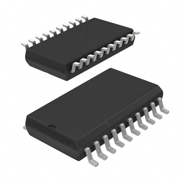
ICGOO电子元器件商城为您提供74ABT541D,602由NXP Semiconductors设计生产,在icgoo商城现货销售,并且可以通过原厂、代理商等渠道进行代购。 74ABT541D,602价格参考。NXP Semiconductors74ABT541D,602封装/规格:逻辑 - 缓冲器,驱动器,接收器,收发器, Buffer, Non-Inverting 1 Element 8 Bit per Element 3-State Output 20-SO。您可以下载74ABT541D,602参考资料、Datasheet数据手册功能说明书,资料中有74ABT541D,602 详细功能的应用电路图电压和使用方法及教程。
型号为 74ABT541D,602 的芯片由 NXP USA Inc. 生产,属于 逻辑 IC - 缓冲器、驱动器、接收器、收发器 类别。它是一款 具有三态输出的8位缓冲器/线路驱动器,广泛应用于数字电路设计中。

 主要应用场景包括:

1. 数据总线缓冲与隔离
   用于在不同总线之间提供缓冲和隔离作用,防止信号过载或干扰,提高系统的稳定性和可靠性。

2. 存储器接口控制
   常用于连接微处理器、存储器模块(如RAM、ROM)之间的地址或数据总线,增强驱动能力,延长传输距离。

3. 工业控制系统
   在PLC、工控机等设备中作为数据路径上的缓冲元件,确保高速信号完整性和抗噪能力。

4. 通信设备中的信号调理
   可用于信号放大、整形和电平转换,适用于需要增强信号驱动能力的场合。

5. 嵌入式系统扩展接口
   在嵌入式系统中用于扩展I/O端口,提升外设连接能力。

该器件支持宽温度范围和高驱动电流能力,适合工业级应用环境。采用 SOIC-20 封装,便于贴片安装,适用于自动化生产流程。
| 参数 | 数值 |
| 产品目录 | 集成电路 (IC)半导体 |
| 描述 | IC BUFF/DVR TRI-ST 8BIT 20SOIC缓冲器和线路驱动器 OCTAL BUFFR/DRVR 3ST |
| 产品分类 | |
| 品牌 | NXP Semiconductors |
| 产品手册 | |
| 产品图片 |
|
| rohs | 符合RoHS无铅 / 符合限制有害物质指令(RoHS)规范要求 |
| 产品系列 | 逻辑集成电路,缓冲器和线路驱动器,NXP Semiconductors 74ABT541D,60274ABT |
| 数据手册 | |
| 产品型号 | 74ABT541D,602 |
| PCN封装 | |
| PCN组件/产地 | |
| 产品培训模块 | http://www.digikey.cn/PTM/IndividualPTM.page?site=cn&lang=zhs&ptm=24983 |
| 产品目录页面 | |
| 产品种类 | 缓冲器和线路驱动器 |
| 传播延迟时间 | 4.6 ns |
| 低电平输出电流 | 64 mA |
| 供应商器件封装 | 20-SO |
| 元件数 | 1 |
| 其它名称 | 568-1375-5 |
| 包装 | 管件 |
| 商标 | NXP Semiconductors |
| 安装类型 | 表面贴装 |
| 安装风格 | SMD/SMT |
| 封装 | Tube |
| 封装/外壳 | 20-SOIC(0.295",7.50mm 宽) |
| 封装/箱体 | SOT-163-20 |
| 工作温度 | -40°C ~ 85°C |
| 工厂包装数量 | 1520 |
| 最大工作温度 | + 85 C |
| 最小工作温度 | - 40 C |
| 极性 | Non-Inverting |
| 标准包装 | 38 |
| 每元件位数 | 8 |
| 每芯片的通道数量 | 8 |
| 电压-电源 | 4.5 V ~ 5.5 V |
| 电流-输出高,低 | 32mA,64mA |
| 电源电压-最大 | 5.5 V |
| 电源电压-最小 | 4.5 V |
| 输入线路数量 | 8 |
| 输出类型 | 3-State |
| 输出线路数量 | 8 |
| 逻辑类型 | Octal Buffer/Line Driver |
| 逻辑系列 | ABT |
| 零件号别名 | 74ABT541D |
| 高电平输出电流 | - 32 mA |


- 商务部:美国ITC正式对集成电路等产品启动337调查
- 曝三星4nm工艺存在良率问题 高通将骁龙8 Gen1或转产台积电
- 太阳诱电将投资9.5亿元在常州建新厂生产MLCC 预计2023年完工
- 英特尔发布欧洲新工厂建设计划 深化IDM 2.0 战略
- 台积电先进制程称霸业界 有大客户加持明年业绩稳了
- 达到5530亿美元!SIA预计今年全球半导体销售额将创下新高
- 英特尔拟将自动驾驶子公司Mobileye上市 估值或超500亿美元
- 三星加码芯片和SET,合并消费电子和移动部门,撤换高东真等 CEO
- 三星电子宣布重大人事变动 还合并消费电子和移动部门
- 海关总署:前11个月进口集成电路产品价值2.52万亿元 增长14.8%


PDF Datasheet 数据手册内容提取
INTEGRATED CIRCUITS 74ABT541 Octal buffer/line driver (3-State) Product specification 1998 Jan 16 Supersedes data of 1996 Sep 10 IC23 Data Handbook (cid:1)(cid:6)(cid:7)(cid:8)(cid:7)(cid:12)(cid:14) (cid:2)(cid:5)(cid:9)(cid:7)(cid:3)(cid:11)(cid:10)(cid:4)(cid:16)(cid:3)(cid:15)(cid:11)(cid:13)(cid:14)
Philips Semiconductors Product specification Octal buffer/line driver (3-State) 74ABT541 FEATURES • ESD protection exceeds 2000 V per MIL STD 883 Method 3015 • Octal bus interface and 200 V per Machine Model • • Functions similar to the ’ABT241 Live insertion/extraction permitted • Provides ideal interface and increases fan-out of MOS DESCRIPTION Microprocessors • The 74ABT541 high-performance BiCMOS device combines low Efficient pinout to facilitate PC board layout static and dynamic power dissipation with high speed and high • 3-State buffer outputs sink 64mA and source 32mA output drive. •Power-up 3-State The 74ABT541 device is an octal buffer that is ideal for driving bus • lines. The outputs are all capable of sinking 64mA and sourcing Latch-up protection exceeds 500mA per Jedec JC40.2 Std 17 32mA. The device features input and outputs on opposite sides of the package to facilitate printed circuit board layout. QUICK REFERENCE DATA CONDITIONS SYMBOL PARAMETER Tamb = 25°C; GND = 0V TYPICAL UNIT ttPPLHHL PArno tpoa Ygantion delay CL = 50pF; VCC = 5V 2.9 ns CIN Input capacitance VI = 0V or VCC 4 pF COUT Output capacitance Outputs disabled; VO = 0V or VCC 7 pF ICCZ Total supply current Outputs disabled; VCC = 5.5V 500 nA ORDERING INFORMATION PACKAGES TEMPERATURE RANGE OUTSIDE NORTH AMERICA NORTH AMERICA DWG NUMBER 20-Pin Plastic DIP –40°C to +85°C 74ABT541 N 74ABT541 N SOT146-1 20-Pin plastic SO –40°C to +85°C 74ABT541 D 74ABT541 D SOT163-1 20-Pin Plastic SSOP Type II –40°C to +85°C 74ABT541 DB 74ABT541 DB SOT339-1 20-Pin PlasticTSSOP Type I –40°C to +85°C 74ABT541 PW 74ABT541PW DH SOT360-1 PIN CONFIGURATION LOGIC SYMBOL 1 OE0 19 OE1 OE0 1 20 VCC 2 18 A0 Y0 A0 2 19 OE1 3 17 A1 3 18 Y0 A1 Y1 A2 4 17 Y1 4 16 A2 Y2 A3 5 16 Y2 5 15 A3 Y3 A4 6 15 Y3 6 14 A5 7 14 Y4 A4 Y4 A6 8 13 Y5 7 13 A5 Y5 A7 9 12 Y6 8 12 GND 10 11 Y7 A6 Y6 9 11 A7 Y7 SA00202 SA00203 1998 Jan 16 2 853-1458 18864
Philips Semiconductors Product specification Octal buffer/line driver (3-State) 74ABT541 LOGIC SYMBOL (IEEE/IEC) PIN DESCRIPTION PIN NUMBER SYMBOL NAME AND FUNCTION 2, 3, 4, 5, 1 & 6, 7, 8, 9 A0 – A7 Data inputs EN 19 18, 17, 16, 15, Y0 – Y7 Data outputs 14, 13, 12, 11 1, 19 OE0, OE1 Output enables 2 18 3 17 10 GND Ground (0V) 4 16 20 VCC Positive supply voltage 5 15 6 14 FUNCTION TABLE 7 13 8 12 INPUTS OUTPUTS 9 11 OE0 OE1 An Yn L L L L SA00204 L L H H X H X Z H X X Z H =High voltage level L =Low voltage level X =Don’t care Z =High impedance ”off” state ABSOLUTE MAXIMUM RATINGS1, 2 SYMBOL PARAMETER CONDITIONS RATING UNIT VCC DC supply voltage –0.5 to +7.0 V IIK DC input diode current VI < 0 –18 mA VI DC input voltage3 –1.2 to +7.0 V IOK DC output diode current VO < 0 –50 mA VOUT DC output voltage3 output in Off or High state –0.5 to +5.5 V IOUT DC output current output in Low state 128 mA Tstg Storage temperature range –65 to 150 °C NOTES: 1. Stresses beyond those listed may cause permanent damage to the device. These are stress ratings only and functional operation of the device at these or any other conditions beyond those indicated under “recommended operating conditions” is not implied. Exposure to absolute-maximum-rated conditions for extended periods may affect device reliability. 2. The performance capability of a high-performance integrated circuit in conjunction with its thermal environment can create junction temperatures which are detrimental to reliability. The maximum junction temperature of this integrated circuit should not exceed 150°C. 3. The input and output voltage ratings may be exceeded if the input and output current ratings are observed. 1998 Jan 16 3
Philips Semiconductors Product specification Octal buffer/line driver (3-State) 74ABT541 RECOMMENDED OPERATING CONDITIONS SYMBOL PARAMETER LIMITS UNIT Min Max VCC DC supply voltage 4.5 5.5 V VI Input voltage 0 VCC V VIH High-level input voltage 2.0 V VIL Low-level Input voltage 0.8 V IOH High-level output current –32 mA IOL Low-level output current 64 mA D t/D v Input transition rise or fall rate 0 5 ns/V Tamb Operating free-air temperature range –40 +85 °C DC ELECTRICAL CHARACTERISTICS LIMITS SYMBOL PARAMETER TEST CONDITIONS Tamb = +25°C Tamtob +=8 –54°C0°C UNIT Min Typ Max Min Max VIK Input clamp voltage VCC = 4.5V; IIK = –18mA –0.9 –1.2 –1.2 V VCC = 4.5V; IOH = –3mA; VI = VIL or VIH 2.5 2.9 2.5 V VOH High-level output voltage VCC = 5.0V; IOH = –3mA; VI = VIL or VIH 3.0 3.4 3.0 V VCC = 4.5V; IOH = –32mA; VI = VIL or VIH 2.0 2.4 2.0 V VOL Low-level output voltage VCC = 4.5V; IOL = 64mA; VI = VIL or VIH 0.42 0.55 0.55 V II Input leakage current VCC = 5.5V; VI = GND or 5.5V ±0.01 ±1.0 ±1.0 m A IOFF Power-off leakage current VCC = 0.0V; VI or VO ≤ 4.5V ±5.0 ±100 ±100 m A IPU/IPD Pouotwpeurt -cuupr/rdeonwt3n 3-state VVCOCE == D2.o0nV’;t VcaOr e= 0.5V; VI = GND or VCC; ±5.0 ±50 ±50 m A IOZH 3-State output High current VCC = 5.5V; VO = 2.7V; VI = VIL or VIH 5.0 50 50 m A IOZL 3-State output Low current VCC = 5.5V; VO = 0.5V; VI = VIL or VIH –5.0 –50 –50 m A ICEX Output High leakage current VCC = 5.5V; VO = 5.5V; VI = GND or VCC 5.0 50 50 m A IO Output current1 VCC = 5.5V; VO = 2.5V –40 –100 –180 –40 –180 mA ICCH VCC = 5.5V; Outputs High, VI = GND or VCC 0.5 250 250 m A ICCL Quiescent supply current VCC = 5.5V; Outputs Low, VI = GND or VCC 24 30 30 mA ICCZ VVCI =C G= N5.D5 Vo;r OVuCtCputs 3-State; 0.5 250 250 m A Outputs enabled, one input at 3.4V, other 0.5 1.5 1.5 mA inputs at VCC or GND; VCC = 5.5V D ICC Aindpduitt ipoinna2l supply current per Ootuhtepru itnsp 3u-tSs taatt eV,C oCn eo rd GatNaD in; pVuCt Ca t= 3 5.4.5VV, 0.5 50 50 m A Outputs 3-State, one enable input at 3.4V, 0.5 1.5 1.5 mA other inputs at VCC or GND; VCC = 5.5V NOTES: 1. Not more than one output should be tested at a time, and the duration of the test should not exceed one second. 2. This is the increase in supply current for each input at 3.4V. 3. This parameter is valid for any VCC between 0V and 2.1V with a transition time of up to 10msec. For VCC = 2.1V to VCC = 5V (cid:1) 10%, a transition time of up to 100m sec is permitted. 1998 Jan 16 4
Philips Semiconductors Product specification Octal buffer/line driver (3-State) 74ABT541 AC CHARACTERISTICS GND = 0V; tR = tF = 2.5ns; CL = 50pF, RL = 500W LIMITS SYMBOL PARAMETER WAVEFORM TVaCmCb == ++52.50°VC TaVmCb C= =– 4+05°.0CV t o± 0+.855V°C UNIT Min Typ Max Min Max tPLH Propagation delay 1 1.0 2.6 4.1 1.0 4.6 ns tPHL An to Yn 1.0 2.9 4.2 1.0 4.6 tPZH Output enable time 2 1.1 3.1 4.8 1.1 5.3 ns tPZL to High and Low level 2.1 4.4 5.9 2.1 6.4 tPHZ Output disable time 2 2.1 5.1 6.6 2.1 7.1 ns tPLZ from High and Low level 1.7 4.7 6.2 1.7 6.7 AC WAVEFORMS VM = 1.5V, VIN = GND to 3.0V 3 V OEn VM VM 1.5V 1.5V INPUT INPUT 0 V tPZL tPLZ 3.5V tPLH tPHL Yn VM VOH OUTPUT VOL + 0.3V tPZH tPHZ VOL 1.5V 1.5V VOH OUTPUT Yn VOH – 0.3V VOL OUTPUT VM SA00028 0V SA00206 Waveform 1. Waveforms Showing the Input (An) to Output (Yn) Waveform 2. Waveforms Showing the 3-State Output Enable Propagation Delays and Disable Times TEST CIRCUIT AND WAVEFORMS 7 V 500 W S1 From Output Open Under Test GND CL = 50 pF 500 W Load Circuit TEST S1 tpd open tPLZ/tPZL 7 V tPHZ/tPZH open DEFINITIONS CL = Load capacitance includes jig and probe capacitance; see AC CHARACTERISTICS for value. SA00012 1998 Jan 16 5
Philips Semiconductors Product specification Octal buffer/line driver (3-State) 74ABT541 DIP20: plastic dual in-line package; 20 leads (300 mil) SOT146-1 1998 Jan 16 6
Philips Semiconductors Product specification Octal buffer/line driver (3-State) 74ABT541 SO20: plastic small outline package; 20 leads; body width 7.5 mm SOT163-1 1998 Jan 16 7
Philips Semiconductors Product specification Octal buffer/line driver (3-State) 74ABT541 SSOP20: plastic shrink small outline package; 20 leads; body width 5.3 mm SOT339-1 1998 Jan 16 8
Philips Semiconductors Product specification Octal buffer/line driver (3-State) 74ABT541 TSSOP20: plastic thin shrink small outline package; 20 leads; body width 4.4 mm SOT360-1 1998 Jan 16 9
Philips Semiconductors Product specification Octal buffer/line driver (3-State) 74ABT541 NOTES 1998 Jan 16 10
Philips Semiconductors Product specification Octal buffer/line driver (3-State) 74ABT541 Data sheet status Data sheet Product Definition [1] status status Objective Development This data sheet contains the design target or goal specifications for product development. specification Specification may change in any manner without notice. Preliminary Qualification This data sheet contains preliminary data, and supplementary data will be published at a later date. specification Philips Semiconductors reserves the right to make chages at any time without notice in order to improve design and supply the best possible product. Product Production This data sheet contains final specifications. Philips Semiconductors reserves the right to make specification changes at any time without notice in order to improve design and supply the best possible product. [1] Please consult the most recently issued datasheet before initiating or completing a design. Definitions Short-form specification — The data in a short-form specification is extracted from a full data sheet with the same type number and title. For detailed information see the relevant data sheet or data handbook. Limiting values definition — Limiting values given are in accordance with the Absolute Maximum Rating System (IEC 134). Stress above one or more of the limiting values may cause permanent damage to the device. These are stress ratings only and operation of the device at these or at any other conditions above those given in the Characteristics sections of the specification is not implied. Exposure to limiting values for extended periods may affect device reliability. Application information — Applications that are described herein for any of these products are for illustrative purposes only. Philips Semiconductors make no representation or warranty that such applications will be suitable for the specified use without further testing or modification. Disclaimers Life support — These products are not designed for use in life support appliances, devices or systems where malfunction of these products can reasonably be expected to result in personal injury. Philips Semiconductors customers using or selling these products for use in such applications do so at their own risk and agree to fully indemnify Philips Semiconductors for any damages resulting from such application. Right to make changes — Philips Semiconductors reserves the right to make changes, without notice, in the products, including circuits, standard cells, and/or software, described or contained herein in order to improve design and/or performance. Philips Semiconductors assumes no responsibility or liability for the use of any of these products, conveys no license or title under any patent, copyright, or mask work right to these products, and makes no representations or warranties that these products are free from patent, copyright, or mask work right infringement, unless otherwise specified. Philips Semiconductors Copyright Philips Electronics North America Corporation 1998 811 East Arques Avenue All rights reserved. Printed in U.S.A. P.O. Box 3409 Sunnyvale, California 94088–3409 print code Date of release: 05-96 Telephone 800-234-7381 Document order number: 9397-750-03614 (cid:1)(cid:6)(cid:7)(cid:8)(cid:7)(cid:12)(cid:14) (cid:2)(cid:5)(cid:9)(cid:7)(cid:3)(cid:11)(cid:10)(cid:4)(cid:16)(cid:3)(cid:15)(cid:11)(cid:13)(cid:14) yyyy mmm dd 11