ICGOO在线商城 > 集成电路(IC) > 逻辑 - 缓冲器,驱动器,接收器,收发器 > CLVTH16245AQDGGREP
 Datasheet下载
- 型号: CLVTH16245AQDGGREP
- 制造商: Texas Instruments
- 库位|库存: xxxx|xxxx
- 要求:
| 数量阶梯 | 香港交货 | 国内含税 |
| +xxxx | $xxxx | ¥xxxx |
查看当月历史价格
查看今年历史价格
CLVTH16245AQDGGREP产品简介:
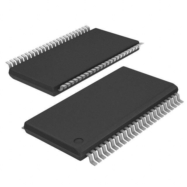
ICGOO电子元器件商城为您提供CLVTH16245AQDGGREP由Texas Instruments设计生产,在icgoo商城现货销售,并且可以通过原厂、代理商等渠道进行代购。 CLVTH16245AQDGGREP价格参考¥10.97-¥22.48。Texas InstrumentsCLVTH16245AQDGGREP封装/规格:逻辑 - 缓冲器,驱动器,接收器,收发器, Transceiver, Non-Inverting 2 Element 8 Bit per Element 3-State Output 48-TSSOP。您可以下载CLVTH16245AQDGGREP参考资料、Datasheet数据手册功能说明书,资料中有CLVTH16245AQDGGREP 详细功能的应用电路图电压和使用方法及教程。
CLVTH16245AQDGGREP 是由 Texas Instruments(德州仪器)生产的一款逻辑器件,属于缓冲器、驱动器、接收器和收发器类别。以下是其典型应用场景:

 1. 高速数据传输
   - CLVTH16245AQDGGREP 支持高速数据传输,适用于需要快速信号传递的系统。例如,在计算机主板或通信设备中,用于在不同模块之间传输数据信号。

 2. 总线扩展与隔离
   - 该器件可以作为总线缓冲器或驱动器,用于扩展系统中的数据总线容量。它能够增强信号强度,确保长距离传输时信号不失真,同时减少噪声干扰。
   - 在多设备共享同一总线的情况下,可以实现信号隔离,避免信号冲突。

 3. 工业控制
   - 在工业自动化领域,这款芯片可用于控制信号的放大和转换。例如,在 PLC(可编程逻辑控制器)或数据采集系统中,将传感器信号转换为适合处理的逻辑电平。

 4. 通信接口设计
   - 该器件支持多种通信协议的接口设计,例如 UART、SPI 或 I2C 等。它可以作为信号中继器或转换器,用于连接不同电平标准的设备。

 5. 嵌入式系统
   - 在嵌入式系统中,CLVTH16245AQDGGREP 可用于优化信号完整性,尤其是在高密度电路板上。它能够提高信号驱动能力,确保系统稳定运行。

 6. 测试与测量设备
   - 在测试仪器中,如示波器或多用表,该芯片可用于信号调理和放大,以适应不同的输入范围和负载条件。

 7. 汽车电子
   - 由于其高性能和可靠性,该器件也可用于汽车电子系统中,例如车载信息娱乐系统、驾驶辅助系统或诊断工具中的信号处理。

 总结
CLVTH16245AQDGGREP 的主要应用场景集中在需要高速、可靠信号传输的领域,包括计算机、通信、工业控制、嵌入式系统和汽车电子等。它的高性能和灵活性使其成为许多复杂电子系统中的关键组件。
| 参数 | 数值 |
| 产品目录 | 集成电路 (IC)半导体 |
| 描述 | IC 16BIT BUS/TXRX 3.3V48-TSSOP总线收发器 Mil Enhance 3.3V ABT 16B Bus Xcvrs |
| 产品分类 | |
| 品牌 | Texas Instruments |
| 产品手册 | |
| 产品图片 |
|
| rohs | 符合RoHS库存产品核实请求 / 库存产品核实请求 |
| 产品系列 | 逻辑集成电路,总线收发器,Texas Instruments CLVTH16245AQDGGREP74LVTH |
| 数据手册 | |
| 产品型号 | CLVTH16245AQDGGREP |
| 产品目录页面 | |
| 产品种类 | 总线收发器 |
| 传播延迟时间 | 4.5 ns |
| 低电平输出电流 | 24 mA |
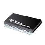
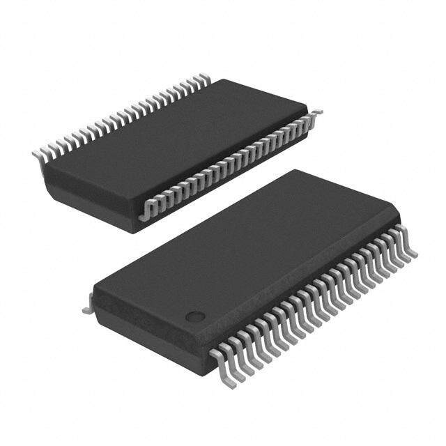
| 供应商器件封装 | 48-TSSOP |
| 元件数 | 2 |
| 其它名称 | 296-18098-6 |
| 功能 | Bus Transceiver |
| 包装 | Digi-Reel® |
| 单位重量 | 223.200 mg |
| 商标 | Texas Instruments |
| 安装类型 | 表面贴装 |
| 安装风格 | SMD/SMT |
| 封装 | Reel |
| 封装/外壳 | 48-TFSOP(0.240",6.10mm 宽) |
| 封装/箱体 | TSSOP-48 |
| 工作温度 | -40°C ~ 125°C |
| 工厂包装数量 | 2000 |
| 最大工作温度 | + 125 C |
| 最小工作温度 | - 40 C |
| 极性 | Non-Inverting |
| 标准包装 | 1 |
| 每元件位数 | 8 |
| 每芯片的通道数量 | 16 |
| 电压-电源 | 2.7 V ~ 3.6 V |
| 电流-输出高,低 | 24mA,24mA |
| 电源电压-最大 | 3.6 V |
| 电源电压-最小 | 2.7 V |
| 电路数量 | 2 |
| 系列 | SN74LVTH16245A-EP |
| 输入电平 | TTL/CMOS |
| 输出电平 | LVTTL |
| 输出类型 | 3-State |
| 逻辑类型 | 收发器,非反相 |
| 逻辑系列 | LVT |
| 高电平输出电流 | - 24 mA |


- 商务部:美国ITC正式对集成电路等产品启动337调查
- 曝三星4nm工艺存在良率问题 高通将骁龙8 Gen1或转产台积电
- 太阳诱电将投资9.5亿元在常州建新厂生产MLCC 预计2023年完工
- 英特尔发布欧洲新工厂建设计划 深化IDM 2.0 战略
- 台积电先进制程称霸业界 有大客户加持明年业绩稳了
- 达到5530亿美元!SIA预计今年全球半导体销售额将创下新高
- 英特尔拟将自动驾驶子公司Mobileye上市 估值或超500亿美元
- 三星加码芯片和SET,合并消费电子和移动部门,撤换高东真等 CEO
- 三星电子宣布重大人事变动 还合并消费电子和移动部门
- 海关总署:前11个月进口集成电路产品价值2.52万亿元 增长14.8%


PDF Datasheet 数据手册内容提取
SN74LVTH16245A-EP 3.3-V ABT 16-BIT BUS TRANSCEIVER WITH 3-STATE OUTPUTS www.ti.com SCAS693G–APRIL2003–REVISEDOCTOBER2006 FEATURES DGG, DGV, OR DLPACKAGE • ControlledBaseline (TOPVIEW) – OneAssembly – OneTestSite 1DIR 1 48 1OE 1B1 2 47 1A1 – OneFabricationSite 1B2 3 46 1A2 • EnhancedDiminishingManufacturing GND 4 45 GND Sources(DMS)Support 1B3 5 44 1A3 • EnhancedProduct-ChangeNotification 1B4 6 43 1A4 • QualificationPedigree (1) V 7 42 V CC CC • MemberoftheTexasInstrumentsWidebus™ 1B5 8 41 1A5 Family 1B6 9 40 1A6 • State-of-the-ArtAdvancedBiCMOS GND 10 39 GND 1B7 11 38 1A7 Technology(ABT)Designfor3.3-VOperation 1B8 12 37 1A8 andLowStatic-PowerDissipation 2B1 13 36 2A1 • SupportsMixed-ModeSignalOperation(5-V 2B2 14 35 2A2 InputandOutputVoltagesWith3.3-VV ) CC GND 15 34 GND • SupportsUnregulatedBatteryOperation 2B3 16 33 2A3 Downto2.7V 2B4 17 32 2A4 • TypicalV (OutputGroundBounce)<0.8V V 18 31 V atVCC=3O.3LPV,TA=25(cid:176) C 2BC5C 19 30 2ACC5 • DistributedV andGNDPinsMinimize 2B6 20 29 2A6 CC High-SpeedSwitchingNoise GND 21 28 GND • Flow-ThroughArchitectureOptimizesPCB 2B7 22 27 2A7 Layout 2B8 23 26 2A8 • I andPower-Up3-StateSupportHot 2DIR 24 25 2OE off Insertion • BusHoldonDataInputsEliminatestheNeed forExternalPullup/PulldownResistors • Latch-UpPerformanceExceeds500mAPer JESD17 • ESDProtectionExceedsJESD22 – 2000-VHuman-BodyModel(A114-A) – 200-VMachineModel(A115-A) (1) ComponentqualificationinaccordancewithJEDECand industrystandardstoensurereliableoperationoveran extendedtemperaturerange.Thisincludes,butisnotlimited to,HighlyAcceleratedStressTest(HAST)orbiased85/85, temperaturecycle,autoclaveorunbiasedHAST, electromigration,bondintermetalliclife,andmoldcompound life.Suchqualificationtestingshouldnotbeviewedas justifyinguseofthiscomponentbeyondspecified performanceandenvironmentallimits. Pleasebeawarethatanimportantnoticeconcerningavailability,standardwarranty,anduseincriticalapplicationsofTexas Instrumentssemiconductorproductsanddisclaimerstheretoappearsattheendofthisdatasheet. WidebusisatrademarkofTexasInstruments. PRODUCTIONDATAinformationiscurrentasofpublicationdate. Copyright©2003–2006,TexasInstrumentsIncorporated Products conform to specifications per the terms of the Texas Instruments standard warranty. Production processing does not necessarilyincludetestingofallparameters.
SN74LVTH16245A-EP 3.3-V ABT 16-BIT BUS TRANSCEIVER WITH 3-STATE OUTPUTS www.ti.com SCAS693G–APRIL2003–REVISEDOCTOBER2006 DESCRIPTION/ORDERING INFORMATION The SN74LVTH16245A is a 16-bit (dual-octal) noninverting 3-state transceiver designed for low-voltage (3.3-V) V operation,butwiththecapabilitytoprovideaTTLinterfacetoa5-Vsystemenvironment. CC This device can be used as two 8-bit transceivers or one 16-bit transceiver. It allows data transmission from the A bus to the B bus or from the B bus to the A bus, depending on the logic level at the direction-control (DIR) input.Theoutput-enable(OE)inputcanbeusedtodisablethedevicessothatthebuseseffectivelyareisolated. Active bus-hold circuitry holds unused or undriven inputs at a valid logic state. Use of pullup or pulldown resistorswiththebus-holdcircuitryisnotrecommended. When V is between 0 V and 1.5 V, the device is in the high-impedance state during power up or power down. CC However, to ensure the high-impedance state above 1.5 V, OE should be tied to V through a pullup resistor; CC theminimumvalueoftheresistorisdeterminedbythecurrent-sinkingcapabilityofthedriver. This device is fully specified for hot-insertion applications using I and power-up 3-state. The I circuitry off off disables the outputs, preventing damaging current backflow through the device when it is powered down. The power-up 3-state circuitry places the outputs in the high-impedance state during power up and power down, whichpreventsdriverconflict. GQLOR ZQLPACKAGE TERMINALASSIGNMENTS(1) (TOPVIEW) 1 2 3 4 5 6 1 2 3 4 5 6 A 1DIR NC NC NC NC 1OE A B 1B2 1B1 GND GND 1A1 1A2 B C 1B4 1B3 V V 1A3 1A4 CC CC C D 1B6 1B5 GND GND 1A5 1A6 D E 1B8 1B7 1A7 1A8 F 2B1 2B2 12A2 2A1 E G 2B3 2B4 GND GND 2A4 2A3 F H 2B5 2B6 V V 2A6 2A5 CC CC G J 2B7 2B8 GND GND 2A8 2A7 H K 2DIR NC NC NC NC 2OE J K (1) NC–nointernalconnection ORDERINGINFORMATION T PACKAGE(1) ORDERABLEPARTNUMBER TOP-SIDEMARKING A SSOP–DL Tapeandreel CLVTH16245AQDLREP LH16245AEP –40(cid:176) Cto125(cid:176) C TSSOP–DGG Tapeandreel CLVTH16245AQDGGREP LH16245AEP TVSOP–DGV Tapeandreel CLVTH16245AIDGVREP LL245AEP –40(cid:176) Cto85(cid:176) C VFBGA–GQL CLVTH16245AIGQLREP VFBGA–ZQL Tapeandreel LL245AEP CLVTH16245AIZQLREP (Pb-free) –55(cid:176) Cto125(cid:176) C SSOP–DL Tapeandreel CLVTH16245AMDLREP LH16245AEP (1) Packagedrawings,standardpackingquantities,thermaldata,symbolization,andPCBdesignguidelinesareavailableat www.ti.com/sc/package. 2 SubmitDocumentationFeedback
SN74LVTH16245A-EP 3.3-V ABT 16-BIT BUS TRANSCEIVER WITH 3-STATE OUTPUTS www.ti.com SCAS693G–APRIL2003–REVISEDOCTOBER2006 FUNCTIONTABLE (each8-bitsection) INPUTS OPERATION OE DIR L L BdatatoAbus L H AdatatoBbus H X Isolation LOGICDIAGRAM(POSITIVELOGIC) 1 24 1DIR 2DIR 48 25 1OE 2OE 47 36 1A1 2A1 2 13 1B1 2B1 To Seven Other Channels To Seven Other Channels Absolute Maximum Ratings(1) overoperatingfree-airtemperaturerange(unlessotherwisenoted) MIN MAX UNIT V Supplyvoltagerange –0.5 4.6 V CC V Inputvoltagerange(2) –0.5 7 V I V Voltagerangeappliedtoanyoutputinthehigh-impedanceorpower-offstate(2) –0.5 7 V O V Voltagerangeappliedtoanyoutputinthehighstate(2) –0.5 V +0.5 V O CC SN74LVTH16245A(Q/M) 96 I Currentintoanyoutputinthelowstate mA O SN74LVTH16245AI 128 SN74LVTH16245A(Q/M) 48 I Currentintoanyoutputinthehighstate(3) mA O SN74LVTH16245AI 64 I Inputclampcurrent V <0 –50 mA IK I I Outputclampcurrent V <0 –50 mA OK O DGGpackage 70 DGVpackage 58 q Packagethermalimpedance(4) (cid:176) C/W JA DLpackage 63 GQL/ZQLpackage 42 T Storagetemperaturerange –65 150 (cid:176) C stg (1) Stressesbeyondthoselistedunder"absolutemaximumratings"maycausepermanentdamagetothedevice.Thesearestressratings only,andfunctionaloperationofthedeviceattheseoranyotherconditionsbeyondthoseindicatedunder"recommendedoperating conditions"isnotimplied.Exposuretoabsolute-maximum-ratedconditionsforextendedperiodsmayaffectdevicereliability. (2) Theinputandoutputnegative-voltageratingsmaybeexceedediftheinputandoutputclamp-currentratingsareobserved. (3) ThiscurrentflowsonlywhentheoutputisinthehighstateandV >V . O CC (4) ThepackagethermalimpedanceiscalculatedinaccordancewithJESD51-7. SubmitDocumentationFeedback 3
SN74LVTH16245A-EP 3.3-V ABT 16-BIT BUS TRANSCEIVER WITH 3-STATE OUTPUTS www.ti.com SCAS693G–APRIL2003–REVISEDOCTOBER2006 Recommended Operating Conditions(1) SN74LVTH16245AQ SN74LVTH16245AI SN74LVTH16245AM UNIT MIN MAX MIN MAX MIN MAX V Supplyvoltage 2.7 3.6 2.7 3.6 2.7 3.6 V CC V High-levelinputvoltage 2 2 2 V IH V Low-levelinputvoltage 0.8 0.8 0.8 V IL V Inputvoltage 5.5 5.5 5.5 V I I High-leveloutputcurrent –24 –32 –24 mA OH I Low-leveloutputcurrent 24 64 24 mA OL D t/D v Inputtransitionriseorfallrate Outputsenabled 10 10 10 ns/V D t/D V Power-upramprate 200 200 200 m s/V CC T Operatingfree-airtemperature –40 125 –40 85 –55 125 (cid:176) C A (1) AllunusedcontrolinputsofthedevicemustbeheldatV orGNDtoensureproperdeviceoperation.SeetheTIapplicationreport, CC ImplicationsofSloworFloatingCMOSInputs(SCBA004). 4 SubmitDocumentationFeedback
SN74LVTH16245A-EP 3.3-V ABT 16-BIT BUS TRANSCEIVER WITH 3-STATE OUTPUTS www.ti.com SCAS693G–APRIL2003–REVISEDOCTOBER2006 Electrical Characteristics overoperatingfree-airtemperaturerange(unlessotherwisenoted) SN74LVTH16245AQ SN74LVTH16245AI SN74LVTH16245AM PARAMETER TESTCONDITIONS UNIT MIN TYP(1) MAX MIN TYP(1) MAX MIN TYP(1) MAX V V =2.7V, I =–18mA –1.2 –1.2 –1.2 V IK CC I V =2.7Vto3.6V, V V V CC CC CC CC I =–100m A –0.2 –0.2 –0.2 OH VOH VCC=2.7V, IOH=–8mA 2.4 2.4 2.4 V I =–24mA 2 2 OH V =3.3V CC I =–32mA 2 OH I =100m A 0.2 0.2 0.2 OL V =2.7V CC I =24mA 0.5 0.5 0.5 OL V I =16mA 0.4 0.4 0.4 V OL OL V =3V I =32mA 0.5 CC OL I =64mA 0.55 OL VCC=3.6V, – 1 – 1 – 1 V =V orGND I CC Controlinputs V =0or3.6V, CC 10 10 10 I VI=5.5V m A I V =5.5V 20 20 20 I AorBport(2) V =3.6V V =V 5 1 5 CC I CC V =0 –5 –5 –5 I I VCC=0, – 100 m A off V orV =0to4.5V I O V =0.8V 75 75 75 I V =3V CC I (3) AorBport VI=2V –75 –75 –75 m A I(hold) V =3.6V, 500 CC V =0to3.6V –750 I V =0to1.5V, CC I V =0.5Vto3V, – 100 – 100 – 100 m A OZPU O OE=don'tcare V =1.5Vto0, CC I V =0.5Vto3V, – 100 – 100 – 100 m A OZPD O OE=don'tcare Outputshigh 0.19 0.19 0.19 V =3.6V, CC I =0, Outputslow 5 5 5 I O mA CC V =V or I CC Outputs GND 0.19 0.19 0.19 disabled V =3Vto3.6V, CC D I (4) OneinputatV –0.6V, 0.2 0.2 0.2 mA CC CC OtherinputsatV orGND CC C V =3Vor0 4 4 4 pF i I C V =3Vor0 10 10 10 pF io O (1) AlltypicalvaluesareatV =3.3V,T =25(cid:176) C. CC A (2) UnusedpinsatV orGND CC (3) Thisisthebus-holdmaximumdynamiccurrent.Itistheminimumoverdrivecurrentrequiredtoswitchtheinputfromonestateto another. (4) ThisistheincreaseinsupplycurrentforeachinputthatisatthespecifiedTTLvoltagelevel,ratherthanV orGND. CC SubmitDocumentationFeedback 5
SN74LVTH16245A-EP 3.3-V ABT 16-BIT BUS TRANSCEIVER WITH 3-STATE OUTPUTS www.ti.com SCAS693G–APRIL2003–REVISEDOCTOBER2006 Switching Characteristics overoperatingfree-airtemperaturerange,C =50pF(unlessotherwisenoted)(seeFigure1) L SN74LVTH16245AQ SN74LVTH16245AI SN74LVTH16245AM FROM TO PARAMETER V =3.3V V =3.3V UNIT (INPUT) (OUTPUT) C–C0.3V VCC=2.7V C–C0.3V VCC=2.7V MIN MAX MIN MAX MIN TYP(1) MAX MIN MAX t 0.5 4.5 4.6 1.5 2.3 3.3 3.7 ns PLH AorB BorA t 0.5 4.4 3.9 1.3 2.1 3.3 3.5 PHL t 0.5 6.5 6.6 1.5 2.8 4.5 5.3 ns PZH OE AorB t 0.5 5.4 6.2 1.6 2.9 4.6 5.2 PZL t 1 6.8 7 2.3 3.7 5.1 5.5 ns PHZ OE AorB t 1 6.2 6.3 2.2 3.5 5.1 5.4 PLZ t 0.5 0.5 ns sk(o) (1) AlltypicalvaluesareatV =3.3V,T =25(cid:176) C. CC A 6 SubmitDocumentationFeedback
SN74LVTH16245A-EP 3.3-V ABT 16-BIT BUS TRANSCEIVER WITH 3-STATE OUTPUTS www.ti.com SCAS693G–APRIL2003–REVISEDOCTOBER2006 PARAMETER MEASUREMENT INFORMATION 6 V 500W S1 Open TEST S1 From Output t /t Open Under Test GND PLH PHL t /t 6 V C = 50 pF PLZ PZL (seeL NoteA) 500W tPHZ/tPZH GND 2.7 V LOAD CIRCUIT Timing Input 1.5 V 0 V t w t t su h 2.7 V 2.7 V Input 1.5 V 1.5 V Data Input 1.5 V 1.5 V 0 V 0 V VOLTAGE WAVEFORMS VOLTAGE WAVEFORMS PULSE DURATION SETUPAND HOLD TIMES 2.7 V 2.7 V Output Input 1.5 V 1.5 V 1.5 V 1.5 V Control 0 V 0 V t t t t PLH PHL Output PZL PLZ V 3 V Waveform 1 Output 1.5 V 1.5 V 1.5 V S1 at 6 V V + 0.3 V V (see Note B) OL V tPHL tPLH tPZH tPHZ Output V V Output 1.5 V 1.5 V WSa1v eafto GrmN D2 1.5 V VOH-0.3 V V (see Note B) »0 V VOLTAGE WAVEFORMS VOLTAGE WAVEFORMS PROPAGATION DELAYTIMES ENABLEAND DISABLE TIMES INVERTINGAND NONINVERTING OUTPUTS LOW-AND HIGH-LEVELENABLING NOTES: A. C includes probe and jig capacitance. L B. Waveform1 is for an output with internal conditions such that the output is low, except when disabled by the output control. Waveform 2 is for an output with internal conditions such that the output is high, except when disabled by the output control. C. All input pulses are supplied by generators having the following characteristics: PRR£10 MHz, Z = 59W, t £2.5 ns, t £2.5 ns. O r f D. The outputs are measured one at a time, with one transition per measurement. Figure1.LoadCircuitandVoltageWaveforms SubmitDocumentationFeedback 7
PACKAGE OPTION ADDENDUM www.ti.com 6-Feb-2020 PACKAGING INFORMATION Orderable Device Status Package Type Package Pins Package Eco Plan Lead/Ball Finish MSL Peak Temp Op Temp (°C) Device Marking Samples (1) Drawing Qty (2) (6) (3) (4/5) 8V16245AMDLREPG4 ACTIVE SSOP DL 48 1000 Green (RoHS NIPDAU Level-1-260C-UNLIM -55 to 125 LVTH16245AEP & no Sb/Br) CLVTH16245AMDLREP ACTIVE SSOP DL 48 1000 Green (RoHS NIPDAU Level-1-260C-UNLIM -55 to 125 LVTH16245AEP & no Sb/Br) CLVTH16245AQDGGREP ACTIVE TSSOP DGG 48 2000 Green (RoHS NIPDAU Level-1-260C-UNLIM -40 to 125 LH16245AEP & no Sb/Br) CLVTH16245AQDLREP ACTIVE SSOP DL 48 1000 Green (RoHS NIPDAU Level-1-260C-UNLIM -40 to 125 LH16245AEP & no Sb/Br) V62/04602-01XE ACTIVE SSOP DL 48 1000 Green (RoHS NIPDAU Level-1-260C-UNLIM -40 to 125 LH16245AEP & no Sb/Br) V62/04602-01YE ACTIVE TSSOP DGG 48 2000 Green (RoHS NIPDAU Level-1-260C-UNLIM -40 to 125 LH16245AEP & no Sb/Br) V62/04602-03XE ACTIVE SSOP DL 48 1000 Green (RoHS NIPDAU Level-1-260C-UNLIM -55 to 125 LVTH16245AEP & no Sb/Br) (1) The marketing status values are defined as follows: ACTIVE: Product device recommended for new designs. LIFEBUY: TI has announced that the device will be discontinued, and a lifetime-buy period is in effect. NRND: Not recommended for new designs. Device is in production to support existing customers, but TI does not recommend using this part in a new design. PREVIEW: Device has been announced but is not in production. Samples may or may not be available. OBSOLETE: TI has discontinued the production of the device. (2) RoHS: TI defines "RoHS" to mean semiconductor products that are compliant with the current EU RoHS requirements for all 10 RoHS substances, including the requirement that RoHS substance do not exceed 0.1% by weight in homogeneous materials. Where designed to be soldered at high temperatures, "RoHS" products are suitable for use in specified lead-free processes. TI may reference these types of products as "Pb-Free". RoHS Exempt: TI defines "RoHS Exempt" to mean products that contain lead but are compliant with EU RoHS pursuant to a specific EU RoHS exemption. Green: TI defines "Green" to mean the content of Chlorine (Cl) and Bromine (Br) based flame retardants meet JS709B low halogen requirements of <=1000ppm threshold. Antimony trioxide based flame retardants must also meet the <=1000ppm threshold requirement. (3) MSL, Peak Temp. - The Moisture Sensitivity Level rating according to the JEDEC industry standard classifications, and peak solder temperature. (4) There may be additional marking, which relates to the logo, the lot trace code information, or the environmental category on the device. (5) Multiple Device Markings will be inside parentheses. Only one Device Marking contained in parentheses and separated by a "~" will appear on a device. If a line is indented then it is a continuation of the previous line and the two combined represent the entire Device Marking for that device. Addendum-Page 1
PACKAGE OPTION ADDENDUM www.ti.com 6-Feb-2020 (6) Lead/Ball Finish - Orderable Devices may have multiple material finish options. Finish options are separated by a vertical ruled line. Lead/Ball Finish values may wrap to two lines if the finish value exceeds the maximum column width. Important Information and Disclaimer:The information provided on this page represents TI's knowledge and belief as of the date that it is provided. TI bases its knowledge and belief on information provided by third parties, and makes no representation or warranty as to the accuracy of such information. Efforts are underway to better integrate information from third parties. TI has taken and continues to take reasonable steps to provide representative and accurate information but may not have conducted destructive testing or chemical analysis on incoming materials and chemicals. TI and TI suppliers consider certain information to be proprietary, and thus CAS numbers and other limited information may not be available for release. In no event shall TI's liability arising out of such information exceed the total purchase price of the TI part(s) at issue in this document sold by TI to Customer on an annual basis. OTHER QUALIFIED VERSIONS OF SN74LVTH16245A-EP : •Catalog: SN74LVTH16245A •Automotive: SN74LVTH16245A-Q1 •Military: SN54LVTH16245A NOTE: Qualified Version Definitions: •Catalog - TI's standard catalog product •Automotive - Q100 devices qualified for high-reliability automotive applications targeting zero defects •Military - QML certified for Military and Defense Applications Addendum-Page 2
PACKAGE MATERIALS INFORMATION www.ti.com 11-Mar-2017 TAPE AND REEL INFORMATION *Alldimensionsarenominal Device Package Package Pins SPQ Reel Reel A0 B0 K0 P1 W Pin1 Type Drawing Diameter Width (mm) (mm) (mm) (mm) (mm) Quadrant (mm) W1(mm) CLVTH16245AMDLREP SSOP DL 48 1000 330.0 32.4 11.35 16.2 3.1 16.0 32.0 Q1 CLVTH16245AQDGGREP TSSOP DGG 48 2000 330.0 24.4 8.6 13.0 1.8 12.0 24.0 Q1 CLVTH16245AQDLREP SSOP DL 48 1000 330.0 32.4 11.35 16.2 3.1 16.0 32.0 Q1 PackMaterials-Page1
PACKAGE MATERIALS INFORMATION www.ti.com 11-Mar-2017 *Alldimensionsarenominal Device PackageType PackageDrawing Pins SPQ Length(mm) Width(mm) Height(mm) CLVTH16245AMDLREP SSOP DL 48 1000 367.0 367.0 55.0 CLVTH16245AQDGGREP TSSOP DGG 48 2000 367.0 367.0 45.0 CLVTH16245AQDLREP SSOP DL 48 1000 367.0 367.0 55.0 PackMaterials-Page2
None
MECHANICAL DATA MTSS003D – JANUARY 1995 – REVISED JANUARY 1998 DGG (R-PDSO-G**) PLASTIC SMALL-OUTLINE PACKAGE 48 PINS SHOWN 0,27 0,50 0,08 M 0,17 48 25 6,20 8,30 6,00 7,90 0,15 NOM Gage Plane 0,25 1 24 0°–8° A 0,75 0,50 Seating Plane 0,15 1,20 MAX 0,10 0,05 PINS ** 48 56 64 DIM A MAX 12,60 14,10 17,10 A MIN 12,40 13,90 16,90 4040078/F 12/97 NOTES: A. All linear dimensions are in millimeters. B. This drawing is subject to change without notice. C. Body dimensions do not include mold protrusion not to exceed 0,15. D. Falls within JEDEC MO-153 • POST OFFICE BOX 655303 DALLAS, TEXAS 75265
IMPORTANTNOTICEANDDISCLAIMER TI PROVIDES TECHNICAL AND RELIABILITY DATA (INCLUDING DATASHEETS), DESIGN RESOURCES (INCLUDING REFERENCE DESIGNS), APPLICATION OR OTHER DESIGN ADVICE, WEB TOOLS, SAFETY INFORMATION, AND OTHER RESOURCES “AS IS” AND WITH ALL FAULTS, AND DISCLAIMS ALL WARRANTIES, EXPRESS AND IMPLIED, INCLUDING WITHOUT LIMITATION ANY IMPLIED WARRANTIES OF MERCHANTABILITY, FITNESS FOR A PARTICULAR PURPOSE OR NON-INFRINGEMENT OF THIRD PARTY INTELLECTUAL PROPERTY RIGHTS. These resources are intended for skilled developers designing with TI products. You are solely responsible for (1) selecting the appropriate TI products for your application, (2) designing, validating and testing your application, and (3) ensuring your application meets applicable standards, and any other safety, security, or other requirements. These resources are subject to change without notice. TI grants you permission to use these resources only for development of an application that uses the TI products described in the resource. Other reproduction and display of these resources is prohibited. No license is granted to any other TI intellectual property right or to any third party intellectual property right. TI disclaims responsibility for, and you will fully indemnify TI and its representatives against, any claims, damages, costs, losses, and liabilities arising out of your use of these resources. TI’s products are provided subject to TI’s Terms of Sale (www.ti.com/legal/termsofsale.html) or other applicable terms available either on ti.com or provided in conjunction with such TI products. TI’s provision of these resources does not expand or otherwise alter TI’s applicable warranties or warranty disclaimers for TI products. Mailing Address: Texas Instruments, Post Office Box 655303, Dallas, Texas 75265 Copyright © 2020, Texas Instruments Incorporated