ICGOO在线商城 > 集成电路(IC) > 嵌入式 - FPGA(现场可编程门阵列) > 5CGXFC7C6F23I7N
 Datasheet下载
- 型号: 5CGXFC7C6F23I7N
- 制造商: altera
- 库位|库存: xxxx|xxxx
- 要求:
| 数量阶梯 | 香港交货 | 国内含税 |
| +xxxx | $xxxx | ¥xxxx |
查看当月历史价格
查看今年历史价格
5CGXFC7C6F23I7N产品简介:
ICGOO电子元器件商城为您提供5CGXFC7C6F23I7N由altera设计生产,在icgoo商城现货销售,并且可以通过原厂、代理商等渠道进行代购。 5CGXFC7C6F23I7N价格参考。altera5CGXFC7C6F23I7N封装/规格:嵌入式 - FPGA(现场可编程门阵列), 。您可以下载5CGXFC7C6F23I7N参考资料、Datasheet数据手册功能说明书,资料中有5CGXFC7C6F23I7N 详细功能的应用电路图电压和使用方法及教程。
Intel型号为5CGXFC7C6F23I7N的FPGA(现场可编程门阵列)属于Cyclone V系列,具体是Cyclone V GX FPGA家族的一员。该型号集成了丰富的逻辑资源、数字信号处理(DSP)模块以及多种接口功能,适用于嵌入式系统开发和高性能计算领域。以下是其主要应用场景:

1. 通信设备:可用于小型基站、无线接入点或数据包处理等场景,支持灵活的协议适配和高效的数据传输。

2. 工业自动化:在工业控制中实现复杂的实时任务调度、运动控制以及机器视觉处理,满足高可靠性和低延迟需求。

3. 物联网(IoT)网关:作为边缘计算的核心组件,提供数据采集、预处理及加密功能,同时连接多种传感器与云端服务。

4. 视频与图像处理:适用于需要快速图像分析的应用,例如高清摄像头中的图像增强、压缩编码等功能。

5. 医疗设备:用于便携式超声波机、监护仪等医疗器械中,完成信号采集、处理和显示等工作。

6. 汽车电子:支持高级驾驶辅助系统(ADAS)、车载信息娱乐系统等领域,具备强大的数据处理能力和接口扩展性。

7. 消费类电子产品:如游戏机、无人机控制器等产品中用作主控芯片或协处理器,提升整体性能。

这款FPGA凭借其较低功耗、紧凑封装以及综合成本优势,在上述各类应用场合均表现出色,尤其适合对性价比有较高要求但又需要一定灵活性和技术深度的项目。
| 参数 | 数值 |
| 产品目录 | 集成电路 (IC) |
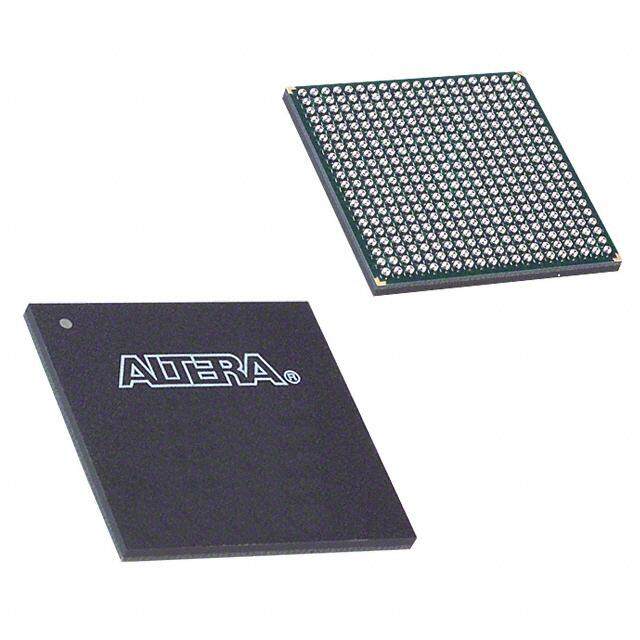
| 描述 | IC FPGA 240 I/O 484FBGA |
| 产品分类 | |
| I/O数 | 240 |
| LAB/CLB数 | 56480 |
| 品牌 | Altera |
| 数据手册 | 点击此处下载产品Datasheet点击此处下载产品Datasheet点击此处下载产品Datasheet点击此处下载产品Datasheet点击此处下载产品Datasheet点击此处下载产品Datasheet |
| 产品图片 |
|
| 产品型号 | 5CGXFC7C6F23I7N |
| rohs | 无铅 / 符合限制有害物质指令(RoHS)规范要求 |
| 产品系列 | Cyclone® V GX |
| 产品培训模块 | http://www.digikey.cn/PTM/IndividualPTM.page?site=cn&lang=zhs&ptm=30447 |
| 供应商器件封装 | 484-FBGA(23x23) |
| 其它名称 | 544-2763 |
| 安装类型 | 表面贴装 |
| 封装/外壳 | 484-BGA |
| 工作温度 | -40°C ~ 100°C |
| 总RAM位数 | 7880704 |
| 栅极数 | - |
| 标准包装 | 60 |
| 特色产品 | http://www.digikey.cn/product-highlights/zh/cyclone-v-fpga-family/52211 |
| 电压-电源 | 1.07 V ~ 1.13 V |
| 逻辑元件/单元数 | 149500 |


- 商务部:美国ITC正式对集成电路等产品启动337调查
- 曝三星4nm工艺存在良率问题 高通将骁龙8 Gen1或转产台积电
- 太阳诱电将投资9.5亿元在常州建新厂生产MLCC 预计2023年完工
- 英特尔发布欧洲新工厂建设计划 深化IDM 2.0 战略
- 台积电先进制程称霸业界 有大客户加持明年业绩稳了
- 达到5530亿美元!SIA预计今年全球半导体销售额将创下新高
- 英特尔拟将自动驾驶子公司Mobileye上市 估值或超500亿美元
- 三星加码芯片和SET,合并消费电子和移动部门,撤换高东真等 CEO
- 三星电子宣布重大人事变动 还合并消费电子和移动部门
- 海关总署:前11个月进口集成电路产品价值2.52万亿元 增长14.8%

PDF Datasheet 数据手册内容提取
Cyclone V Device Overview Subscribe CV-51001 | 2018.05.07 Send Feedback Latest document on the web: PDF | HTML
Contents Contents Cyclone V Device Overview.................................................................................................3 Key Advantages of Cyclone V Devices.............................................................................3 Summary of Cyclone V Features.....................................................................................4 Cyclone V Device Variants and Packages.........................................................................5 Cyclone V E........................................................................................................5 Cyclone V GX.....................................................................................................7 Cyclone V GT......................................................................................................9 Cyclone V SE....................................................................................................12 Cyclone V SX....................................................................................................14 Cyclone V ST....................................................................................................15 I/O Vertical Migration for Cyclone V Devices...................................................................18 Adaptive Logic Module................................................................................................18 Variable-Precision DSP Block........................................................................................19 Embedded Memory Blocks...........................................................................................21 Types of Embedded Memory...............................................................................21 Embedded Memory Capacity in Cyclone V Devices.................................................21 Embedded Memory Configurations.......................................................................22 Clock Networks and PLL Clock Sources..........................................................................22 FPGA General Purpose I/O...........................................................................................23 PCIe Gen1 and Gen2 Hard IP.......................................................................................24 External Memory Interface..........................................................................................24 Hard and Soft Memory Controllers.......................................................................24 External Memory Performance............................................................................25 HPS External Memory Performance......................................................................25 Low-Power Serial Transceivers......................................................................................25 Transceiver Channels.........................................................................................25 PMA Features................................................................................................... 26 PCS Features....................................................................................................27 SoC with HPS.............................................................................................................28 HPS Features....................................................................................................28 FPGA Configuration and Processor Booting............................................................30 Hardware and Software Development..................................................................31 Dynamic and Partial Reconfiguration.............................................................................31 Dynamic Reconfiguration....................................................................................31 Partial Reconfiguration.......................................................................................31 Enhanced Configuration and Configuration via Protocol....................................................32 Power Management....................................................................................................33 Document Revision History for Cyclone V Device Overview...............................................33 Cyclone V Device Overview 2
CV-51001 | 2018.05.07 Cyclone V Device Overview The Cyclone® V devices are designed to simultaneously accommodate the shrinking power consumption, cost, and time-to-market requirements; and the increasing bandwidth requirements for high-volume and cost-sensitive applications. Enhanced with integrated transceivers and hard memory controllers, the Cyclone V devices are suitable for applications in the industrial, wireless and wireline, military, and automotive markets. Related Information Cyclone V Device Handbook: Known Issues Lists the planned updates to the Cyclone V Device Handbook chapters. Key Advantages of Cyclone V Devices Table 1. Key Advantages of the Cyclone V Device Family Advantage Supporting Feature Lower power consumption • Built on TSMC's 28 nm low-power (28LP) process technology and includes an abundance of hard intellectual property (IP) blocks • Up to 40% lower power consumption than the previous generation device Improved logic integration and • 8-input adaptive logic module (ALM) differentiation capabilities • Up to 13.59 megabits (Mb) of embedded memory • Variable-precision digital signal processing (DSP) blocks Increased bandwidth capacity • 3.125 gigabits per second (Gbps) and 6.144 Gbps transceivers • Hard memory controllers Hard processor system (HPS) • Tight integration of a dual-core Arm Cortex-A9 MPCore processor, hard IP, and an with integrated Arm* Cortex*-A9 FPGA in a single Cyclone V system-on-a-chip (SoC) MPCore* processor • Supports over 128 Gbps peak bandwidth with integrated data coherency between the processor and the FPGA fabric Lowest system cost • Requires only two core voltages to operate • Available in low-cost wirebond packaging • Includes innovative features such as Configuration via Protocol (CvP) and partial reconfiguration Intel Corporation. All rights reserved. Intel, the Intel logo, Altera, Arria, Cyclone, Enpirion, MAX, Nios, Quartus and Stratix words and logos are trademarks of Intel Corporation or its subsidiaries in the U.S. and/or other countries. Intel warrants performance of its FPGA and semiconductor products to current specifications in ISO accordance with Intel's standard warranty, but reserves the right to make changes to any products and services 9001:2008 at any time without notice. Intel assumes no responsibility or liability arising out of the application or use of any Registered information, product, or service described herein except as expressly agreed to in writing by Intel. Intel customers are advised to obtain the latest version of device specifications before relying on any published information and before placing orders for products or services. *Other names and brands may be claimed as the property of others.
Cyclone V Device Overview CV-51001 | 2018.05.07 Summary of Cyclone V Features Table 2. Summary of Features for Cyclone V Devices Feature Description Technology • TSMC's 28-nm low-power (28LP) process technology • 1.1 V core voltage Packaging • Wirebond low-halogen packages • Multiple device densities with compatible package footprints for seamless migration between different device densities • RoHS-compliant and leaded(1)options High-performance Enhanced 8-input ALM with four registers FPGA fabric Internal memory • M10K—10-kilobits (Kb) memory blocks with soft error correction code (ECC) blocks • Memory logic array block (MLAB)—640-bit distributed LUTRAM where you can use up to 25% of the ALMs as MLAB memory Embedded Hard IP Variable-precision DSP • Native support for up to three signal processing precision levels blocks (three 9 x 9, two 18 x 18, or one 27 x 27 multiplier) in the same variable-precision DSP block • 64-bit accumulator and cascade • Embedded internal coefficient memory • Preadder/subtractor for improved efficiency Memory controller DDR3, DDR2, and LPDDR2 with 16 and 32 bit ECC support Embedded transceiver PCI Express* (PCIe*) Gen2 and Gen1 (x1, x2, or x4) hard IP with I/O multifunction support, endpoint, and root port Clock networks • Up to 550 MHz global clock network • Global, quadrant, and peripheral clock networks • Clock networks that are not used can be powered down to reduce dynamic power Phase-locked loops • Precision clock synthesis, clock delay compensation, and zero delay buffering (ZDB) (PLLs) • Integer mode and fractional mode FPGA General-purpose • 875 megabits per second (Mbps) LVDS receiver and 840 Mbps LVDS transmitter I/Os (GPIOs) • 400 MHz/800 Mbps external memory interface • On-chip termination (OCT) • 3.3 V support with up to 16 mA drive strength Low-power high-speed • 614 Mbps to 6.144 Gbps integrated transceiver speed serial interface • Transmit pre-emphasis and receiver equalization • Dynamic partial reconfiguration of individual channels HPS • Single or dual-core Arm Cortex-A9 MPCore processor-up to 925 MHz maximum frequency with (Cyclone V SE, SX, support for symmetric and asymmetric multiprocessing and ST devices only) • Interface peripherals—10/100/1000 Ethernet media access control (EMAC), USB 2.0 On-The-GO (OTG) controller, quad serial peripheral interface (QSPI) flash controller, NAND flash controller, Secure Digital/MultiMediaCard (SD/MMC) controller, UART, controller area network (CAN), serial peripheral interface (SPI), I2C interface, and up to 85 HPS GPIO interfaces • System peripherals—general-purpose timers, watchdog timers, direct memory access (DMA) controller, FPGA configuration manager, and clock and reset managers • On-chip RAM and boot ROM continued... (1) Contact Intel for availability. Cyclone V Device Overview 4
Cyclone V Device Overview CV-51001 | 2018.05.07 Feature Description • HPS–FPGA bridges—include the FPGA-to-HPS, HPS-to-FPGA, and lightweight HPS-to-FPGA bridges that allow the FPGA fabric to issue transactions to slaves in the HPS, and vice versa • FPGA-to-HPS SDRAM controller subsystem—provides a configurable interface to the multiport front end (MPFE) of the HPS SDRAM controller • Arm CoreSight™ JTAG debug access port, trace port, and on-chip trace storage Configuration • Tamper protection—comprehensive design protection to protect your valuable IP investments • Enhanced advanced encryption standard (AES) design security features • CvP • Dynamic reconfiguration of the FPGA • Active serial (AS) x1 and x4, passive serial (PS), JTAG, and fast passive parallel (FPP) x8 and x16 configuration options • Internal scrubbing (2) • Partial reconfiguration (3) Cyclone V Device Variants and Packages Table 3. Device Variants for the Cyclone V Device Family Variant Description Cyclone V E Optimized for the lowest system cost and power requirement for a wide spectrum of general logic and DSP applications Cyclone V GX Optimized for the lowest cost and power requirement for 614 Mbps to 3.125 Gbps transceiver applications Cyclone V GT The FPGA industry’s lowest cost and lowest power requirement for 6.144 Gbps transceiver applications Cyclone V SE SoC with integrated Arm-based HPS Cyclone V SX SoC with integrated Arm-based HPS and 3.125 Gbps transceivers Cyclone V ST SoC with integrated Arm-based HPS and 6.144 Gbps transceivers Cyclone V E This section provides the available options, maximum resource counts, and package plan for the Cyclone V E devices. The information in this section is correct at the time of publication. For the latest information and to get more details, refer to the Product Selector Guide. Related Information Product Selector Guide Provides the latest information about Intel products. (2) The SEU internal scrubbing feature is available for Cyclone V E, GX, SE, and SX devices with the "SC" suffix in the part number. For device availability and ordering, contact your local Intel sales representatives. (3) The partial reconfiguration feature is available for Cyclone V E, GX, SE, and SX devices with the "SC" suffix in the part number. For device availability and ordering, contact your local Intel® sales representatives. Cyclone V Device Overview 5
Cyclone V Device Overview CV-51001 | 2018.05.07 Available Options Figure 1. Sample Ordering Code and Available Options for Cyclone V E Devices The SEU internal scrubbing feature is available for Cyclone V E, GX, SE, and SX devices with the "SC" suffix in the part number. For device availability and ordering, contact your local Intel sales representatives. Package Type F : FineLine BGA (FBGA) U : Ultra FineLine BGA (UBGA) Embedded Hard IPs M : Micro FineLine BGA (MBGA) B : No hard PCIe or hard Operating Temperature memory controller C : Commercial (T = 0° C to 85° C) F : No hard PCIe and maximum J I : Industrial (T = -40° C to 100° C) 2 hard memory controllers J A : Automotive (T = -40° C to 125° C) J Family Signature 5C E F A9 F 31 C 7 N Optional Suffix 5C : Cyclone V Indicates specific device options or shipment method Family Variant Package Code N : Lead-free packaging E : Enhanced logic/memory FBGA Package Type Contact Intel for availability of leaded options Member Code 17 : 256 pins ES : Engineering sample 23 : 484 pins A2 : 25K logic elements 27 : 672 pins SC : Internal scrubbing support A4 : 49K logic elements 31 : 896 pins A5 : 77K logic elements FPGA Fabric Speed Grade A7 : 150K logic elements UBGA Package Type 6 (fastest) A9 : 301K logic elements 15 : 324 pins 7 19 : 484 pins 8 MBGA Package Type 13 : 383 pins 15 : 484 pins Maximum Resources Table 4. Maximum Resource Counts for Cyclone V E Devices Resource Member Code A2 A4 A5 A7 A9 Logic Elements (LE) (K) 25 49 77 150 301 ALM 9,430 18,480 29,080 56,480 113,560 Register 37,736 73,920 116,320 225,920 454,240 Memory (Kb) M10K 1,760 3,080 4,460 6,860 12,200 MLAB 196 303 424 836 1,717 Variable-precision DSP Block 25 66 150 156 342 18 x 18 Multiplier 50 132 300 312 684 PLL 4 4 6 7 8 GPIO 224 224 240 480 480 LVDS Transmitter 56 56 60 120 120 Receiver 56 56 60 120 120 Hard Memory Controller 1 1 2 2 2 Cyclone V Device Overview 6
Cyclone V Device Overview CV-51001 | 2018.05.07 Related Information True LVDS Buffers in Devices, I/O Features in Cyclone V Devices Provides the number of LVDS channels in each device package. Package Plan Table 5. Package Plan for Cyclone V E Devices Member M383 M484 U324 F256 U484 F484 F672 F896 Code (13 mm) (15 mm) (15 mm) (17 mm) (19 mm) (23 mm) (27 mm) (31 mm) GPIO GPIO GPIO GPIO GPIO GPIO GPIO GPIO A2 223 — 176 128 224 224 — — A4 223 — 176 128 224 224 — — A5 175 — — — 224 240 — — A7 — 240 — — 240 240 336 480 A9 — — — — 240 224 336 480 Cyclone V GX This section provides the available options, maximum resource counts, and package plan for the Cyclone V GX devices. The information in this section is correct at the time of publication. For the latest information and to get more details, refer to the Product Selector Guide. Related Information Product Selector Guide Provides the latest information about Intel products. Cyclone V Device Overview 7
Cyclone V Device Overview CV-51001 | 2018.05.07 Available Options Figure 2. Sample Ordering Code and Available Options for Cyclone V GX Devices The SEU internal scrubbing feature is available for Cyclone V E, GX, SE, and SX devices with the "SC" suffix in the part number. For device availability and ordering, contact your local Intel sales representatives. Package Type Transceiver Count F : FineLine BGA (FBGA) B : 3 U : Ultra FineLine BGA (UBGA) Embedded Hard IPs F : 4 M : Micro FineLine BGA (MBGA) B : No hard PCIe or hard A : 5 Operating Temperature memory controller C : 6 F : Maximum 2 hard PCIe and D : 9 C : Commercial (TJ = 0° C to 85° C) 2 hard memory controllers E : 12 I : Industrial (TJ = -40° C to 100° C) A : Automotive (T = -40° C to 125° C) J Family Signature 5C GX F C9 E 6 F 35 C 7 N 5C : Cyclone V Optional Suffix Family Variant Indicates specific device Package Code GX : 3-Gbps transceivers options or shipment method FBGA Package Type N : Lead-free packaging 23 : 484 pins Member Code Con t act Intel for availability 27 : 672 pins C3 : 36K logic elements Transceiver 31 : 896 pins of leaded options C4 : 50K logic elements Speed Grade 35 : 1,152 pins ES : Engineering sample C5 : 77K logic elements 6 : 3.125 Gbps UBGA Package Type SC : Internal scrubbing support C7 : 150K logic elements 7 : 2.5 Gbps 15 : 324 pins C9 : 301K logic elements FPGA Fabric 19 : 484 pins Speed Grade MBGA Package Type 6 (fastest) 11 : 301 pins 7 13 : 383 pins 8 15 : 484 pins Maximum Resources Table 6. Maximum Resource Counts for Cyclone V GX Devices Resource Member Code C3 C4 C5 C7 C9 Logic Elements (LE) (K) 36 50 77 150 301 ALM 13,460 18,860 29,080 56,480 113,560 Register 53,840 75,440 116,320 225,920 454,240 Memory (Kb) M10K 1,350 2,500 4,460 6,860 12,200 MLAB 182 424 424 836 1,717 Variable-precision DSP Block 57 70 150 156 342 18 x 18 Multiplier 114 140 300 312 684 PLL 4 6 6 7 8 3 Gbps Transceiver 3 6 6 9 12 GPIO(4) 208 336 336 480 560 continued... (4) The number of GPIOs does not include transceiver I/Os. In the Intel Quartus® Prime software, the number of user I/Os includes transceiver I/Os. Cyclone V Device Overview 8
Cyclone V Device Overview CV-51001 | 2018.05.07 Resource Member Code C3 C4 C5 C7 C9 LVDS Transmitter 52 84 84 120 140 Receiver 52 84 84 120 140 PCIe Hard IP Block 1 2 2 2 2 Hard Memory Controller 1 2 2 2 2 Related Information True LVDS Buffers in Devices, I/O Features in Cyclone V Devices Provides the number of LVDS channels in each device package. Package Plan Table 7. Package Plan for Cyclone V GX Devices Member M301 M383 M484 U324 U484 Code (11 mm) (13 mm) (15 mm) (15 mm) (19 mm) GPIO XCVR GPIO XCVR GPIO XCVR GPIO XCVR GPIO XCVR C3 — — — — — — 144 3 208 3 C4 129 4 175 6 — — — — 224 6 C5 129 4 175 6 — — — — 224 6 C7 — — — — 240 3 — — 240 6 C9 — — — — — — — — 240 5 Member F484 F672 F896 F1152 Code (23 mm) (27 mm) (31 mm) (35 mm) GPIO XCVR GPIO XCVR GPIO XCVR GPIO XCVR C3 208 3 — — — — — — C4 240 6 336 6 — — — — C5 240 6 336 6 — — — — C7 240 6 336 9 480 9 — — C9 224 6 336 9 480 12 560 12 Cyclone V GT This section provides the available options, maximum resource counts, and package plan for the Cyclone V GT devices. The information in this section is correct at the time of publication. For the latest information and to get more details, refer to the Product Selector Guide. Related Information Product Selector Guide Provides the latest information about Intel products. Cyclone V Device Overview 9
Cyclone V Device Overview CV-51001 | 2018.05.07 Available Options Figure 3. Sample Ordering Code and Available Options for Cyclone V GT Devices Package Type F : FineLine BGA (FBGA) Transceiver Count U : Ultra FineLine BGA (UBGA) B : 3 M : Micro FineLine BGA (MBGA) F : 4 Operating Temperature Embedded Hard IPs A : 5 C : Commercial (T = 0° C to 85° C) F : Maximum 2 hard PCIe and C : 6 J I : Industrial (T = -40° C to 100° C) 2 hard memory controllers D : 9 J A : Automotive (T = -40° C to 125° C) E : 12 J Family Signature 5C GT F D9 E 5 F 35 C 7 N 5C : Cyclone V Optional Suffix Family Variant Indicates specific device GT : 6-Gbps transceivers Package Code options or shipment method N : Lead-free packaging Member Code FBGA Package Type Contact Intel for availability 23 : 484 pins D5 : 77K logic elements Transceiver 27 : 672 pins of leaded options D7 : 150K logic elements Speed Grade 31 : 896 pins ES : Engineering sample D9 : 301K logic elements 5 : 6.144 Gbps 35 : 1,152 pins FPGA Fabric UBGA Package Type Speed Grade 19 : 484 pins 7 MBGA Package Type 11 : 301 pins 13 : 383 pins 15 : 484 pins Maximum Resources Table 8. Maximum Resource Counts for Cyclone V GT Devices Resource Member Code D5 D7 D9 Logic Elements (LE) (K) 77 150 301 ALM 29,080 56,480 113,560 Register 116,320 225,920 454,240 Memory (Kb) M10K 4,460 6,860 12,200 MLAB 424 836 1,717 Variable-precision DSP Block 150 156 342 18 x 18 Multiplier 300 312 684 PLL 6 7 8 6 Gbps Transceiver 6 9 12 GPIO(5) 336 480 560 LVDS Transmitter 84 120 140 continued... (5) The number of GPIOs does not include transceiver I/Os. In the Intel Quartus Prime software, the number of user I/Os includes transceiver I/Os. Cyclone V Device Overview 10
Cyclone V Device Overview CV-51001 | 2018.05.07 Resource Member Code D5 D7 D9 Receiver 84 120 140 PCIe Hard IP Block 2 2 2 Hard Memory Controller 2 2 2 Related Information True LVDS Buffers in Devices, I/O Features in Cyclone V Devices Provides the number of LVDS channels in each device package. Package Plan Table 9. Package Plan for Cyclone V GT Devices Transceiver counts shown are for transceiver ≤5 Gbps . 6 Gbps transceiver channel count support depends on the package and channel usage. For more information about the 6 Gbps transceiver channel count, refer to the Cyclone V Device Handbook Volume 2: Transceivers. Member M301 M383 M484 U484 Code (11 mm) (13 mm) (15 mm) (19 mm) GPIO XCVR GPIO XCVR GPIO XCVR GPIO XCVR D5 129 4 175 6 — — 224 6 D7 — — — — 240 3 240 6 D9 — — — — — — 240 5 Member F484 F672 F896 F1152 Code (23 mm) (27 mm) (31 mm) (35 mm) GPIO XCVR GPIO XCVR GPIO XCVR GPIO XCVR D5 240 6 336 6 — — — — D7 240 6 336 9 (6) 480 9 (6) — — D9 224 6 336 9 (6) 480 12 (7) 560 12 (7) Related Information 6.144-Gbps Support Capability in Cyclone V GT Devices, Cyclone V Device Handbook Volume 2: Transceivers Provides more information about 6 Gbps transceiver channel count. (6) If you require CPRI (at 6.144 Gbps) and PCIe Gen2 transmit jitter compliance, Intel recommends that you use only up to three full-duplex transceiver channels for CPRI, and up to six full-duplex channels for PCIe Gen2. The CMU channels are not considered full-duplex channels. (7) If you require CPRI (at 6.144 Gbps) and PCIe Gen2 transmit jitter compliance, Intel recommends that you use only up to three full-duplex transceiver channels for CPRI, and up to eight full-duplex channels for PCIe Gen2. The CMU channels are not considered full-duplex channels. Cyclone V Device Overview 11
Cyclone V Device Overview CV-51001 | 2018.05.07 Cyclone V SE This section provides the available options, maximum resource counts, and package plan for the Cyclone V SE devices. The information in this section is correct at the time of publication. For the latest information and to get more details, refer to the Product Selector Guide. Related Information Product Selector Guide Provides the latest information about Intel products. Available Options Figure 4. Sample Ordering Code and Available Options for Cyclone V SE Devices The SEU internal scrubbing feature is available for Cyclone V E, GX, SE, and SX devices with the "SC" suffix in the part number. For device availability and ordering, contact your local Intel sales representatives. Cyclone V SE and SX low-power devices (L power option) offer 30% static power reduction for devices with 25K LE and 40K LE, and 20% static power reduction for devices with 85K LE and 110K LE. Package Type Operating Temperature F : FineLine BGA (FBGA) C : Commercial (TJ = 0° C to 85° C) U : Ultra FineLine BGA (UBGA) I : Industrial (TJ = -40° C to 100° C) Embedded Hard IPs A : Automotive (TJ = -40° C to 125° C) B : No hard PCIe or hard memory controller Processor Cores M : No hard PCIe and Omit for dual-core S : Single-core 1 hard memory controller Family Signature 5C SE M A6 F 31 C 6 S L N Optional Suffix 5C : Cyclone V Indicates specific device options or shipment method Family Variant Power Option N : Lead-free packaging SE : SoC with enhanced logic/memory Package Code Omit for standard power Contact Intel for availability Member Code FBGA Package Type L : Low power of leaded options A2 : 25K logic elements 31 : 896 pins FPGA Fabric ES : Engineering sample A4 : 40K logic elements UBGA Package Type 6Sp (efaesdt eGsrta)de SC : Internal scrubbing support A5 : 85K logic elements 19 : 484 pins 7 A6 : 110K logic elements 23 : 672 pins 8 Cyclone V Device Overview 12
Cyclone V Device Overview CV-51001 | 2018.05.07 Maximum Resources Table 10. Maximum Resource Counts for Cyclone V SE Devices Resource Member Code A2 A4 A5 A6 Logic Elements (LE) (K) 25 40 85 110 ALM 9,430 15,880 32,070 41,910 Register 37,736 60,376 128,300 166,036 Memory (Kb) M10K 1,400 2,700 3,970 5,570 MLAB 138 231 480 621 Variable-precision DSP Block 36 84 87 112 18 x 18 Multiplier 72 168 174 224 FPGA PLL 5 5 6 6 HPS PLL 3 3 3 3 FPGA GPIO 145 145 288 288 HPS I/O 181 181 181 181 LVDS Transmitter 32 32 72 72 Receiver 37 37 72 72 FPGA Hard Memory Controller 1 1 1 1 HPS Hard Memory Controller 1 1 1 1 Arm Cortex-A9 MPCore Processor Single- or dual- Single- or dual- Single- or dual-core Single- or dual-core core core Related Information True LVDS Buffers in Devices, I/O Features in Cyclone V Devices Provides the number of LVDS channels in each device package. Package Plan Table 11. Package Plan for Cyclone V SE Devices The HPS I/O counts are the number of I/Os in the HPS and does not correlate with the number of HPS-specific I/O pins in the FPGA. Each HPS-specific pin in the FPGA may be mapped to several HPS I/Os. Member Code U484 U672 F896 (19 mm) (23 mm) (31 mm) FPGA GPIO HPS I/O FPGA GPIO HPS I/O FPGA GPIO HPS I/O A2 66 151 145 181 — — A4 66 151 145 181 — — A5 66 151 145 181 288 181 A6 66 151 145 181 288 181 Cyclone V Device Overview 13
Cyclone V Device Overview CV-51001 | 2018.05.07 Cyclone V SX This section provides the available options, maximum resource counts, and package plan for the Cyclone V SX devices. The information in this section is correct at the time of publication. For the latest information and to get more details, refer to the Product Selector Guide. Related Information Product Selector Guide Provides the latest information about Intel products. Available Options Figure 5. Sample Ordering Code and Available Options for Cyclone V SX Devices The SEU internal scrubbing feature is available for Cyclone V E, GX, SE, and SX devices with the "SC" suffix in the part number. For device availability and ordering, contact your local Intel sales representatives. Cyclone V SE and SX low-power devices (L power option) offer 30% static power reduction for devices with 25K LE and 40K LE, and 20% static power reduction for devices with 85K LE and 110K LE. Package Type F : FineLine BGA (FBGA) U : Ultra FineLine BGA (UBGA) Operating Temperature Embedded Hard IPs F : Maximum 2 hard PCIe Transceiver Count C : Commercial (TJ = 0° C to 85° C) controllers and 1 hard C : 6 I : Industrial (TJ = -40° C to 100° C) memory controller D : 9 A : Automotive (TJ = -40° C to 125° C) Family Signature 5C SX F C6 D 6 F 31 C 6 L N Optional Suffix 5C : Cyclone V Indicates specific device Power Option options or shipment method Family Variant Omit for standard power N : Lead-free packaging SX : SoC with 3-Gbps transceivers L : Low power Contact Intel for availability Member Code Package Code of leaded options C2 : 25K logic elements FBGA Package Type FPGA Fabric ES : Engineering sample C4 : 40K logic elements Transceiver 31 : 896 pins Speed Grade SC : Internal scrubbing support C5 : 85K logic elements Speed Grade UBGA Package Type 6 (fastest) C6 : 110K logic elements 6 : 3.125 Gbps 23 : 672 pins 7 8 Maximum Resources Table 12. Maximum Resource Counts for Cyclone V SX Devices Resource Member Code C2 C4 C5 C6 Logic Elements (LE) (K) 25 40 85 110 ALM 9,430 15,880 32,070 41,910 Register 37,736 60,376 128,300 166,036 Memory (Kb) M10K 1,400 2,700 3,970 5,570 MLAB 138 231 480 621 Variable-precision DSP Block 36 84 87 112 18 x 18 Multiplier 72 168 174 224 FPGA PLL 5 5 6 6 continued... Cyclone V Device Overview 14
Cyclone V Device Overview CV-51001 | 2018.05.07 Resource Member Code C2 C4 C5 C6 HPS PLL 3 3 3 3 3 Gbps Transceiver 6 6 9 9 FPGA GPIO (8) 145 145 288 288 HPS I/O 181 181 181 181 LVDS Transmitter 32 32 72 72 Receiver 37 37 72 72 PCIe Hard IP Block 2 2 2 (9) 2 (9) FPGA Hard Memory Controller 1 1 1 1 HPS Hard Memory Controller 1 1 1 1 Arm Cortex-A9 MPCore Processor Dual-core Dual-core Dual-core Dual-core Related Information True LVDS Buffers in Devices, I/O Features in Cyclone V Devices Provides the number of LVDS channels in each device package. Package Plan Table 13. Package Plan for Cyclone V SX Devices The HPS I/O counts are the number of I/Os in the HPS and does not correlate with the number of HPS-specific I/O pins in the FPGA. Each HPS-specific pin in the FPGA may be mapped to several HPS I/Os. Member Code U672 F896 (23 mm) (31 mm) FPGA GPIO HPS I/O XCVR FPGA GPIO HPS I/O XCVR C2 145 181 6 — — — C4 145 181 6 — — — C5 145 181 6 288 181 9 C6 145 181 6 288 181 9 Cyclone V ST This section provides the available options, maximum resource counts, and package plan for the Cyclone V ST devices. The information in this section is correct at the time of publication. For the latest information and to get more details, refer to the Product Selector Guide. (8) The number of GPIOs does not include transceiver I/Os. In the Intel Quartus Prime software, the number of user I/Os includes transceiver I/Os. (9) 1 PCIe Hard IP Block in U672 package. Cyclone V Device Overview 15
Cyclone V Device Overview CV-51001 | 2018.05.07 Related Information Product Selector Guide Provides the latest information about Intel products. Available Options Figure 6. Sample Ordering Code and Available Options for Cyclone V ST Devices Package Type F : FineLine BGA (FBGA) Embedded Hard IPs Operating Temperature F : 2 hard PCIe controllers I : Industrial (T= -40° C to 100° C) Transceiver Count J and 1 hard memory controller D : 9 Family Signature 5C ST F D6 D 5 F 31 C 6 N 5C : Cyclone V Optional Suffix Family Variant Indicates specific device ST : SoC with 6.144-Gbps transceivers Package Code options or shipment method Member Code 31 : 896 pins FPGA Fabric N : Lead-free packaging D5 : 85K logic elements Transceiver Speed Grade Contact Intel for availability of leaded options D6 : 110K logic elements Speed Grade 7 ES : Engineering sample 5 : 6.144 Gbps Maximum Resources Table 14. Maximum Resource Counts for Cyclone V ST Devices Resource Member Code D5 D6 Logic Elements (LE) (K) 85 110 ALM 32,070 41,910 Register 128,300 166,036 Memory (Kb) M10K 3,970 5,570 MLAB 480 621 Variable-precision DSP Block 87 112 18 x 18 Multiplier 174 224 FPGA PLL 6 6 HPS PLL 3 3 6.144 Gbps Transceiver 9 9 FPGA GPIO(10) 288 288 HPS I/O 181 181 LVDS Transmitter 72 72 continued... (10) The number of GPIOs does not include transceiver I/Os. In the Intel Quartus Prime software, the number of user I/Os includes transceiver I/Os. Cyclone V Device Overview 16
Cyclone V Device Overview CV-51001 | 2018.05.07 Resource Member Code D5 D6 Receiver 72 72 PCIe Hard IP Block 2 2 FPGA Hard Memory Controller 1 1 HPS Hard Memory Controller 1 1 Arm Cortex-A9 MPCore Processor Dual-core Dual-core Related Information True LVDS Buffers in Devices, I/O Features in Cyclone V Devices Provides the number of LVDS channels in each device package. Package Plan Table 15. Package Plan for Cyclone V ST Devices • The HPS I/O counts are the number of I/Os in the HPS and does not correlate with the number of HPS- specific I/O pins in the FPGA. Each HPS-specific pin in the FPGA may be mapped to several HPS I/Os. • Transceiver counts shown are for transceiver ≤5 Gbps . 6 Gbps transceiver channel count support depends on the package and channel usage. For more information about the 6 Gbps transceiver channel count, refer to the Cyclone V Device Handbook Volume 2: Transceivers. Member Code F896 (31 mm) FPGA GPIO HPS I/O XCVR D5 288 181 9 (11) D6 288 181 9 (11) Related Information 6.144-Gbps Support Capability in Cyclone V GT Devices, Cyclone V Device Handbook Volume 2: Transceivers Provides more information about 6 Gbps transceiver channel count. (11) If you require CPRI (at 4.9152 Gbps) and PCIe Gen2 transmit jitter compliance, Intel recommends that you use only up to seven full-duplex transceiver channels for CPRI, and up to six full-duplex channels for PCIe Gen2. The CMU channels are not considered full-duplex channels. Cyclone V Device Overview 17
Cyclone V Device Overview CV-51001 | 2018.05.07 I/O Vertical Migration for Cyclone V Devices Figure 7. Vertical Migration Capability Across Cyclone V Device Packages and Densities The arrows indicate the vertical migration paths. The devices included in each vertical migration path are shaded. You can also migrate your design across device densities in the same package option if the devices have the same dedicated pins, configuration pins, and power pins. Member Package Variant Code M301 M383 M484 F256 U324 U484 F484 U672 F672 F896 F1152 A2 A4 Cyclone V E A5 A7 A9 C3 C4 Cyclone V GX C5 C7 C9 D5 Cyclone V GT D7 D9 A2 A4 Cyclone V SE A5 A6 C2 C4 Cyclone V SX C5 C6 D5 Cyclone V ST D6 You can achieve the vertical migration shaded in red if you use only up to 175 GPIOs for the M383 package, and 138 GPIOs for the U672 package. These migration paths are not shown in the Intel Quartus Prime software Pin Migration View. Note: To verify the pin migration compatibility, use the Pin Migration View window in the Intel Quartus Prime software Pin Planner. Adaptive Logic Module Cyclone V devices use a 28 nm ALM as the basic building block of the logic fabric. The ALM, as shown in following figure, uses an 8-input fracturable look-up table (LUT) with four dedicated registers to help improve timing closure in register-rich designs and achieve an even higher design packing capability than previous generations. Cyclone V Device Overview 18
Cyclone V Device Overview CV-51001 | 2018.05.07 Figure 8. ALM for Cyclone V Devices FPGA Device Reg 1 Full 2 Adder 3 Reg 4 Adaptive 5 LUT 6 7 Reg 8 Full Adder Reg You can configure up to 25% of the ALMs in the Cyclone V devices as distributed memory using MLABs. Related Information Embedded Memory Capacity in Cyclone V Devices on page 21 Lists the embedded memory capacity for each device. Variable-Precision DSP Block Cyclone V devices feature a variable-precision DSP block that supports these features: • Configurable to support signal processing precisions ranging from 9 x 9, 18 x 18 and 27 x 27 bits natively • A 64-bit accumulator • A hard preadder that is available in both 18- and 27-bit modes • Cascaded output adders for efficient systolic finite impulse response (FIR) filters • Internal coefficient register banks, 8 deep, for each multiplier in 18- or 27-bit mode • Fully independent multiplier operation • A second accumulator feedback register to accommodate complex multiply- accumulate functions • Fully independent Efficient support for single-precision floating point arithmetic • The inferability of all modes by the Intel Quartus Prime design software Cyclone V Device Overview 19
Cyclone V Device Overview CV-51001 | 2018.05.07 Table 16. Variable-Precision DSP Block Configurations for Cyclone V Devices Usage Example Multiplier Size (Bit) DSP Block Resource Low precision fixed point for video Three 9 x 9 1 applications Medium precision fixed point in FIR Two 18 x 18 1 filters FIR filters and general DSP usage Two 18 x 18 with accumulate 1 High precision fixed- or floating-point One 27 x 27 with accumulate 1 implementations You can configure each DSP block during compilation as independent three 9 x 9, two 18 x 18, or one 27 x 27 multipliers. With a dedicated 64 bit cascade bus, you can cascade multiple variable-precision DSP blocks to implement even higher precision DSP functions efficiently. Table 17. Number of Multipliers in Cyclone V Devices The table lists the variable-precision DSP resources by bit precision for each Cyclone V device. Variant Member Variable- Independent Input and Output 18 x 18 18 x 18 Code precision Multiplications Operator Multiplier Multiplier DSP Block Adder Mode Adder 9 x 9 18 x 18 27 x 27 Summed Multiplier Multiplier Multiplier with 36 bit Input Cyclone V E A2 25 75 50 25 25 25 A4 66 198 132 66 66 66 A5 150 450 300 150 150 150 A7 156 468 312 156 156 156 A9 342 1,026 684 342 342 342 Cyclone V C3 57 171 114 57 57 57 GX C4 70 210 140 70 70 70 C5 150 450 300 150 150 150 C7 156 468 312 156 156 156 C9 342 1,026 684 342 342 342 Cyclone V GT D5 150 450 300 150 150 150 D7 156 468 312 156 156 156 D9 342 1,026 684 342 342 342 Cyclone V SE A2 36 108 72 36 36 36 A4 84 252 168 84 84 84 A5 87 261 174 87 87 87 A6 112 336 224 112 112 112 Cyclone V SX C2 36 108 72 36 36 36 C4 84 252 168 84 84 84 C5 87 261 174 87 87 87 continued... Cyclone V Device Overview 20
Cyclone V Device Overview CV-51001 | 2018.05.07 Variant Member Variable- Independent Input and Output 18 x 18 18 x 18 Code precision Multiplications Operator Multiplier Multiplier DSP Block Adder Mode Adder 9 x 9 18 x 18 27 x 27 Summed Multiplier Multiplier Multiplier with 36 bit Input C6 112 336 224 112 112 112 Cyclone V ST D5 87 261 174 87 87 87 D6 112 336 224 112 112 112 Embedded Memory Blocks The embedded memory blocks in the devices are flexible and designed to provide an optimal amount of small- and large-sized memory arrays to fit your design requirements. Types of Embedded Memory The Cyclone V devices contain two types of memory blocks: • 10 Kb M10K blocks—blocks of dedicated memory resources. The M10K blocks are ideal for larger memory arrays while still providing a large number of independent ports. • 640 bit memory logic array blocks (MLABs)—enhanced memory blocks that are configured from dual-purpose logic array blocks (LABs). The MLABs are ideal for wide and shallow memory arrays. The MLABs are optimized for implementation of shift registers for digital signal processing (DSP) applications, wide shallow FIFO buffers, and filter delay lines. Each MLAB is made up of ten adaptive logic modules (ALMs). In the Cyclone V devices, you can configure these ALMs as ten 32 x 2 blocks, giving you one 32 x 20 simple dual-port SRAM block per MLAB. Embedded Memory Capacity in Cyclone V Devices Table 18. Embedded Memory Capacity and Distribution in Cyclone V Devices M10K MLAB Member Total RAM Bit Variant Code Block RAM Bit (Kb) Block RAM Bit (Kb) (Kb) Cyclone V E A2 176 1,760 314 196 1,956 A4 308 3,080 485 303 3,383 A5 446 4,460 679 424 4,884 A7 686 6,860 1338 836 7,696 A9 1,220 12,200 2748 1,717 13,917 Cyclone V GX C3 135 1,350 291 182 1,532 C4 250 2,500 678 424 2,924 C5 446 4,460 678 424 4,884 C7 686 6,860 1338 836 7,696 C9 1,220 12,200 2748 1,717 13,917 continued... Cyclone V Device Overview 21
Cyclone V Device Overview CV-51001 | 2018.05.07 M10K MLAB Member Total RAM Bit Variant Code Block RAM Bit (Kb) Block RAM Bit (Kb) (Kb) Cyclone V GT D5 446 4,460 679 424 4,884 D7 686 6,860 1338 836 7,696 D9 1,220 12,200 2748 1,717 13,917 Cyclone V SE A2 140 1,400 221 138 1,538 A4 270 2,700 370 231 2,460 A5 397 3,970 768 480 4,450 A6 553 5,530 994 621 6,151 Cyclone V SX C2 140 1,400 221 138 1,538 C4 270 2,700 370 231 2,460 C5 397 3,970 768 480 4,450 C6 553 5,530 994 621 6,151 Cyclone V ST D5 397 3,970 768 480 4,450 D6 553 5,530 994 621 6,151 Embedded Memory Configurations Table 19. Supported Embedded Memory Block Configurations for Cyclone V Devices This table lists the maximum configurations supported for the embedded memory blocks. The information is applicable only to the single-port RAM and ROM modes. Memory Block Depth (bits) Programmable Width MLAB 32 x16, x18, or x20 M10K 256 x40 or x32 512 x20 or x16 1K x10 or x8 2K x5 or x4 4K x2 8K x1 Clock Networks and PLL Clock Sources 550 MHz Cyclone V devices have 16 global clock networks capable of up to operation. The clock network architecture is based on Intel's global, quadrant, and peripheral clock structure. This clock structure is supported by dedicated clock input pins and fractional PLLs. Note: To reduce power consumption, the Intel Quartus Prime software identifies all unused sections of the clock network and powers them down. Cyclone V Device Overview 22
Cyclone V Device Overview CV-51001 | 2018.05.07 PLL Features The PLLs in the Cyclone V devices support the following features: • Frequency synthesis • On-chip clock deskew • Jitter attenuation • Programmable output clock duty cycles • PLL cascading • Reference clock switchover • Programmable bandwidth • User-mode reconfiguration of PLLs • Low power mode for each fractional PLL • Dynamic phase shift • Direct, source synchronous, zero delay buffer, external feedback, and LVDS compensation modes Fractional PLL In addition to integer PLLs, the Cyclone V devices use a fractional PLL architecture. The devices have up to eight PLLs, each with nine output counters. You can use the output counters to reduce PLL usage in two ways: • Reduce the number of oscillators that are required on your board by using fractional PLLs • Reduce the number of clock pins that are used in the device by synthesizing multiple clock frequencies from a single reference clock source If you use the fractional PLL mode, you can use the PLLs for precision fractional-N frequency synthesis—removing the need for off-chip reference clock sources in your design. The transceiver fractional PLLs that are not used by the transceiver I/Os can be used as general purpose fractional PLLs by the FPGA fabric. FPGA General Purpose I/O Cyclone V devices offer highly configurable GPIOs. The following list describes the features of the GPIOs: • Programmable bus hold and weak pull-up • LVDS output buffer with programmable differential output voltage (V ) and OD programmable pre-emphasis • On-chip parallel termination (R OCT) for all I/O banks with OCT calibration to T limit the termination impedance variation • On-chip dynamic termination that has the ability to swap between series and parallel termination, depending on whether there is read or write on a common bus for signal integrity • Easy timing closure support using the hard read FIFO in the input register path, and delay-locked loop (DLL) delay chain with fine and coarse architecture Cyclone V Device Overview 23
Cyclone V Device Overview CV-51001 | 2018.05.07 PCIe Gen1 and Gen2 Hard IP Cyclone V GX, GT, SX, and ST devices contain PCIe hard IP that is designed for performance and ease-of-use. The PCIe hard IP consists of the MAC, data link, and transaction layers. The PCIe hard IP supports PCIe Gen2 and Gen1 end point and root port for up to x4 lane configuration. The PCIe Gen2 x4 support is PCIe-compatible. The PCIe endpoint support includes multifunction support for up to eight functions, as shown in the following figure. The integrated multifunction support reduces the FPGA logic requirements by up to 20,000 LEs for PCIe designs that require multiple peripherals. Figure 9. PCIe Multifunction for Cyclone V Devices External System FPGA Device Host CPU SPI GPIO 2IC USB emoryntroller CoRmopoltex CIe RP PCIe Link CIe EP Mo P P C ee Local Local CAN GbE ATA Bridgto PCI Peripheral 1 Peripheral 2 The Cyclone V PCIe hard IP operates independently from the core logic. This independent operation allows the PCIe link to wake up and complete link training in less than 100 ms while the Cyclone V device completes loading the programming file for the rest of the device. In addition, the PCIe hard IP in the Cyclone V device provides improved end-to-end datapath protection using ECC. External Memory Interface This section provides an overview of the external memory interface in Cyclone V devices. Hard and Soft Memory Controllers Cyclone V devices support up to two hard memory controllers for DDR3, DDR2, and LPDDR2 SDRAM devices. Each controller supports 8 to 32 bit components of up to 4 gigabits (Gb) in density with two chip selects and optional ECC. For the Cyclone V SoC devices, an additional hard memory controller in the HPS supports DDR3, DDR2, and LPDDR2 SDRAM devices. All Cyclone V devices support soft memory controllers for DDR3, DDR2, and LPDDR2 SDRAM devices for maximum flexibility. Cyclone V Device Overview 24
Cyclone V Device Overview CV-51001 | 2018.05.07 External Memory Performance Table 20. External Memory Interface Performance in Cyclone V Devices The maximum and minimum operating frequencies depend on the memory interface standards and the supported delay-locked loop (DLL) frequency listed in the device datasheet. Interface Voltage Maximum Frequency (MHz) Minimum Frequency (V) (MHz) Hard Controller Soft Controller DDR3 SDRAM 1.5 400 303 303 1.35 400 303 303 DDR2 SDRAM 1.8 400 300 167 LPDDR2 SDRAM 1.2 333 300 167 Related Information External Memory Interface Spec Estimator For the latest information and to estimate the external memory system performance specification, use Intel's External Memory Interface Spec Estimator tool. HPS External Memory Performance Table 21. HPS External Memory Interface Performance The hard processor system (HPS) is available in Cyclone V SoC devices only. Interface Voltage (V) HPS Hard Controller (MHz) DDR3 SDRAM 1.5 400 1.35 400 DDR2 SDRAM 1.8 400 LPDDR2 SDRAM 1.2 333 Related Information External Memory Interface Spec Estimator For the latest information and to estimate the external memory system performance specification, use Intel's External Memory Interface Spec Estimator tool. Low-Power Serial Transceivers Cyclone V devices deliver the industry’s lowest power 6.144 Gbps transceivers at an estimated 88 mW maximum power consumption per channel. Cyclone V transceivers are designed to be compliant with a wide range of protocols and data rates. Transceiver Channels The transceivers are positioned on the left outer edge of the device. The transceiver channels consist of the physical medium attachment (PMA), physical coding sublayer (PCS), and clock networks. Cyclone V Device Overview 25
Cyclone V Device Overview CV-51001 | 2018.05.07 Figure 10. Device Chip Overview for Cyclone V GX and GT Devices The figure shows a Cyclone V FPGA with transceivers. Different Cyclone V devices may have a different floorplans than the one shown here. I/O, LVDS, and Memory Interface Hard Memory Controller Transceiver Hard Transceiver PMA Blocks Fractional PLLsHard PCS BlocksPCIe Hard IP Blocks Fractional PLLsLVDS, and Memory Interface TTIrrnaadnnPPPissvTMMMccrieedaAAAiiunvvaeesclrr eCihvFractional PLLaenrnHHPPPeCCCaalsSSSrrdd Clock Networks O, I/ Core Logic Fabric and MLABs M10K Internal Memory Blocks Variable-Precision DSP Blocks Hard Memory Controller I/O, LVDS, and Memory Interface PMA Features To prevent core and I/O noise from coupling into the transceivers, the PMA block is isolated from the rest of the chip—ensuring optimal signal integrity. For the transceivers, you can use the channel PLL of an unused receiver PMA as an additional transmit PLL. Table 22. PMA Features of the Transceivers in Cyclone V Devices Features Capability Backplane support Driving capability up to 6.144 Gbps PLL-based clock recovery Superior jitter tolerance Programmable deserialization and word Flexible deserialization width and configurable word alignment pattern alignment Equalization and pre-emphasis • Up to 14.37 dB of pre-emphasis and up to 4.7 dB of equalization • No decision feedback equalizer (DFE) Ring oscillator transmit PLLs 614 Mbps to 6.144 Gbps Input reference clock range 20 MHz to 400 MHz Transceiver dynamic reconfiguration Allows the reconfiguration of a single channel without affecting the operation of other channels Cyclone V Device Overview 26
Cyclone V Device Overview CV-51001 | 2018.05.07 PCS Features The Cyclone V core logic connects to the PCS through an 8, 10, 16, 20, 32, or 40 bit interface, depending on the transceiver data rate and protocol. Cyclone V devices contain PCS hard IP to support PCIe Gen1 and Gen2, Gbps Ethernet (GbE), Serial RapidIO® (SRIO), and Common Public Radio Interface (CPRI). Most of the standard and proprietary protocols from 614 Mbps to 6.144 Gbps are supported. Table 23. Transceiver PCS Features for Cyclone V Devices PCS Support Data Rates Transmitter Data Path Feature Receiver Data Path Feature (Gbps) 3-Gbps and 6-Gbps Basic 0.614 to 6.144 • Phase compensation FIFO • Word aligner • Byte serializer • Deskew FIFO • 8B/10B encoder • Rate-match FIFO • Transmitter bit-slip • 8B/10B decoder • Byte deserializer • Byte ordering • Receiver phase compensation FIFO PCIe Gen1 2.5 and 5.0 • Dedicated PCIe PHY IP core • Dedicated PCIe PHY IP core (x1, x2, x4) • PIPE 2.0 interface to the core • PIPE 2.0 interface to the core logic logic PCIe Gen2 ( x1, x2, x4)(12) GbE 1.25 • Custom PHY IP core with preset • Custom PHY IP core with preset feature feature • GbE transmitter synchronization • GbE receiver synchronization state machine state machine XAUI (13) 3.125 • Dedicated XAUI PHY IP core • Dedicated XAUI PHY IP core • XAUI synchronization state • XAUI synchronization state HiGig 3.75 machine for bonding four machine for realigning four channels channels SRIO 1.3 and 2.1 1.25 to 3.125 • Custom PHY IP core with preset • Custom PHY IP core with preset feature feature • SRIO version 2.1-compliant x2 • SRIO version 2.1-compliant x2 and x4 channel bonding and x4 deskew state machine SDI, SD/HD, and 3G-SDI 0.27(14), 1.485, Custom PHY IP core with preset Custom PHY IP core with preset and 2.97 feature feature JESD204A 0.3125(15) to 3.125 continued... (12) PCIe Gen2 is supported for Cyclone V GT and ST devices. The PCIe Gen2 x4 support is PCIe-compatible. (13) XAUI is supported through the soft PCS. (14) The 0.27-Gbps data rate is supported using oversampling user logic that you must implement in the FPGA fabric. (15) The 0.3125-Gbps data rate is supported using oversampling user logic that you must implement in the FPGA fabric. Cyclone V Device Overview 27
Cyclone V Device Overview CV-51001 | 2018.05.07 PCS Support Data Rates Transmitter Data Path Feature Receiver Data Path Feature (Gbps) Serial ATA Gen1 and Gen2 1.5 and 3.0 • Custom PHY IP core with preset • Custom PHY IP core with preset feature feature • Electrical idle • Signal detect • Wider spread of asynchronous SSC CPRI 4.1(16) 0.6144 to 6.144 • Dedicated deterministic latency • Dedicated deterministic latency PHY IP core PHY IP core OBSAI RP3 0.768 to 3.072 • Transmitter (TX) manual bit-slip • Receiver (RX) deterministic mode latency state machine V-by-One HS Up to 3.75 Custom PHY IP core • Custom PHY IP core • Wider spread of asynchronous DisplayPort 1.2(17) 1.62 and 2.7 SSC SoC with HPS Each SoC combines an FPGA fabric and an HPS in a single device. This combination delivers the flexibility of programmable logic with the power and cost savings of hard IP in these ways: • Reduces board space, system power, and bill of materials cost by eliminating a discrete embedded processor • Allows you to differentiate the end product in both hardware and software, and to support virtually any interface standard • Extends the product life and revenue through in-field hardware and software updates HPS Features The HPS consists of a dual-core Arm Cortex-A9 MPCore processor, a rich set of peripherals, and a shared multiport SDRAM memory controller, as shown in the following figure. (16) High-voltage output mode (1000-BASE-CX) is not supported. (17) Pending characterization. Cyclone V Device Overview 28
Cyclone V Device Overview CV-51001 | 2018.05.07 Figure 11. HPS with Dual-Core Arm Cortex-A9 MPCore Processor Configuration Lightweight FPGA Fabric Controller FPGA-to-HPS HPS-to-FPGA HPS-to-FPGA FPGA-to-HPS SDRAM FPGA HPS Manager Debug MPU Subsystem Access Port ARM Cortex-A9 MPCore ETR CPU0 CPU1 (Trace) ARM Cortex-A9 ARM Cortex-A9 Multiport SD/MMC with NEON/FPU, with NEON/FPU, DDR SDRAM Controller 32 KB Instruction Cache, 32 KB Instruction Cache, Controller 32 KB Data Cache, and 32 KB Data Cache, and Ethernet with Memory Management Memory Management MAC (2x) Optional ECC Unit Unit Level 3 USB ACP SCU Interconnect OTG (2x) NAND Flash Level 2 Cache (512 KB) Controller DMA STM Controller 64 KB Boot ROM 64 KB On-Chip RAM Peripherals (UART, Timer, I2C, Watchdog Timer, GPIO, SPI, Clock Manager, Reset Manager, Scan Manager, System Manager, and Quad SPI Flash Controller) System Peripherals and Debug Access Port Each Ethernet MAC, USB OTG, NAND flash controller, and SD/MMC controller module has an integrated DMA controller. For modules without an integrated DMA controller, an additional DMA controller module provides up to eight channels of high-bandwidth data transfers. Peripherals that communicate off-chip are multiplexed with other peripherals at the HPS pin level. This allows you to choose which peripherals to interface with other devices on your PCB. The debug access port provides interfaces to industry standard JTAG debug probes and supports Arm CoreSight debug and core traces to facilitate software development. Cyclone V Device Overview 29
Cyclone V Device Overview CV-51001 | 2018.05.07 HPS–FPGA AXI Bridges The HPS–FPGA bridges, which support the Advanced Microcontroller Bus Architecture (AMBA®) Advanced eXtensible Interface (AXI™) specifications, consist of the following bridges: • FPGA-to-HPS AXI bridge—a high-performance bus supporting 32, 64, and 128 bit data widths that allows the FPGA fabric to issue transactions to slaves in the HPS. • HPS-to-FPGA AXI bridge—a high-performance bus supporting 32, 64, and 128 bit data widths that allows the HPS to issue transactions to slaves in the FPGA fabric. • Lightweight HPS-to-FPGA AXI bridge—a lower latency 32 bit width bus that allows the HPS to issue transactions to slaves in the FPGA fabric. This bridge is primarily used for control and status register (CSR) accesses to peripherals in the FPGA fabric. The HPS–FPGA AXI bridges allow masters in the FPGA fabric to communicate with slaves in the HPS logic, and vice versa. For example, the HPS-to-FPGA AXI bridge allows you to share memories instantiated in the FPGA fabric with one or both microprocessors in the HPS, while the FPGA-to-HPS AXI bridge allows logic in the FPGA fabric to access the memory and peripherals in the HPS. Each HPS–FPGA bridge also provides asynchronous clock crossing for data transferred between the FPGA fabric and the HPS. HPS SDRAM Controller Subsystem The HPS SDRAM controller subsystem contains a multiport SDRAM controller and DDR PHY that are shared between the FPGA fabric (through the FPGA-to-HPS SDRAM interface), the level 2 (L2) cache, and the level 3 (L3) system interconnect. The FPGA-to-HPS SDRAM interface supports AMBA AXI and Avalon® Memory-Mapped (Avalon-MM) interface standards, and provides up to six individual ports for access by masters implemented in the FPGA fabric. To maximize memory performance, the SDRAM controller subsystem supports command and data reordering, deficit round-robin arbitration with aging, and high-priority bypass features. The SDRAM controller subsystem supports DDR2, DDR3, or LPDDR2 devices up to 4 Gb in density operating at up to 400 MHz (800 Mbps data rate). FPGA Configuration and Processor Booting The FPGA fabric and HPS in the SoC are powered independently. You can reduce the clock frequencies or gate the clocks to reduce dynamic power, or shut down the entire FPGA fabric to reduce total system power. You can configure the FPGA fabric and boot the HPS independently, in any order, providing you with more design flexibility: • You can boot the HPS independently. After the HPS is running, the HPS can fully or partially reconfigure the FPGA fabric at any time under software control. The HPS can also configure other FPGAs on the board through the FPGA configuration controller. • You can power up both the HPS and the FPGA fabric together, configure the FPGA fabric first, and then boot the HPS from memory accessible to the FPGA fabric. Cyclone V Device Overview 30
Cyclone V Device Overview CV-51001 | 2018.05.07 Note: Although the FPGA fabric and HPS are on separate power domains, the HPS must remain powered up during operation while the FPGA fabric can be powered up or down as required. Related Information Cyclone V Device Family Pin Connection Guidelines Provides detailed information about power supply pin connection guidelines and power regulator sharing. Hardware and Software Development For hardware development, you can configure the HPS and connect your soft logic in the FPGA fabric to the HPS interfaces using the Platform Designer (Standard) system integration tool in the Intel Quartus Prime software. For software development, the Arm-based SoC devices inherit the rich software development ecosystem available for the Arm Cortex-A9 MPCore processor. The software development process for Intel SoCs follows the same steps as those for other SoC devices from other manufacturers. Support for Linux, VxWorks®, and other operating systems is available for the SoCs. For more information on the operating systems support availability, contact the Intel sales team. You can begin device-specific firmware and software development on the Intel SoC Virtual Target. The Virtual Target is a fast PC-based functional simulation of a target development system—a model of a complete development board that runs on a PC. The Virtual Target enables the development of device-specific production software that can run unmodified on actual hardware. Related Information International Altera Sales Support Offices Dynamic and Partial Reconfiguration The Cyclone V devices support dynamic reconfiguration and partial reconfiguration. Dynamic Reconfiguration The dynamic reconfiguration feature allows you to dynamically change the transceiver data rates, PMA settings, or protocols of a channel, without affecting data transfer on adjacent channels. This feature is ideal for applications that require on-the-fly multiprotocol or multirate support. You can reconfigure the PMA and PCS blocks with dynamic reconfiguration. Partial Reconfiguration Note: The partial reconfiguration feature is available for Cyclone V E, GX, SE, and SX devices with the "SC" suffix in the part number. For device availability and ordering, contact your local Intel sales representatives. Partial reconfiguration allows you to reconfigure part of the device while other sections of the device remain operational. This capability is important in systems with critical uptime requirements because it allows you to make updates or adjust functionality without disrupting services. Cyclone V Device Overview 31
Cyclone V Device Overview CV-51001 | 2018.05.07 Apart from lowering cost and power consumption, partial reconfiguration increases the effective logic density of the device because placing device functions that do not operate simultaneously is not necessary. Instead, you can store these functions in external memory and load them whenever the functions are required. This capability reduces the size of the device because it allows multiple applications on a single device—saving the board space and reducing the power consumption. Intel simplifies the time-intensive task of partial reconfiguration by building this capability on top of the proven incremental compile and design flow in the Intel Quartus Prime design software. With the Intel solution, you do not need to know all the intricate device architecture details to perform a partial reconfiguration. Partial reconfiguration is supported through the FPP x16 configuration interface. You can seamlessly use partial reconfiguration in tandem with dynamic reconfiguration to enable simultaneous partial reconfiguration of both the device core and transceivers. Enhanced Configuration and Configuration via Protocol Cyclone V devices support 1.8 V, 2.5 V, 3.0 V, and 3.3 V programming voltages and several configuration schemes. Table 24. Configuration Schemes and Features Supported by Cyclone V Devices Mode Data Max Clock Max Data Decompressi Design Partial Remote Width Rate Rate on Security Reconfigurat System (MHz) (Mbps) ion(18) Update AS through the EPCS 1 bit, 4 100 — Yes Yes — Yes and EPCQ serial bits configuration device PS through CPLD or 1 bit 125 125 Yes Yes — — external microcontroller FPP 8 bits 125 — Yes Yes — Parallel flash loader 16 bits 125 — Yes Yes Yes CvP (PCIe) x1, x2, — — Yes Yes Yes — and x4 lanes JTAG 1 bit 33 33 — — — — Instead of using an external flash or ROM, you can configure the Cyclone V devices through PCIe using CvP. The CvP mode offers the fastest configuration rate and flexibility with the easy-to-use PCIe hard IP block interface. The Cyclone V CvP implementation conforms to the PCIe 100 ms power-up-to-active time requirement. Related Information Configuration via Protocol (CvP) Implementation in Intel FPGAs User Guide Provides more information about CvP. (18) The partial reconfiguration feature is available for Cyclone V E, GX, SE, and SX devices with the "SC" suffix in the part number. For device availability and ordering, contact your local Intel sales representatives. Cyclone V Device Overview 32
Cyclone V Device Overview CV-51001 | 2018.05.07 Power Management Leveraging the FPGA architectural features, process technology advancements, and transceivers that are designed for power efficiency, the Cyclone V devices consume less power than previous generation Cyclone FPGAs: • Total device core power consumption—less by up to 40%. • Transceiver channel power consumption—less by up to 50%. Additionally, Cyclone V devices contain several hard IP blocks that reduce logic resources and deliver substantial power savings of up to 25% less power than equivalent soft implementations. Document Revision History for Cyclone V Device Overview Document Changes Version 2018.05.07 • Added the low power option ("L" suffix) for Cyclone V SE and Cyclone V SX devices in the Sample Ordering Code and Available Options diagrams. • Rebranded as Intel. Date Version Changes December 2017 2017.12.18 • Updated ALM resources for Cyclone V E, Cyclone V SE, Cyclone V SX, and Cyclone V ST devices. June 2016 2016.06.10 Updated Cyclone V GT speed grade to –7 in Sample Ordering Code and Available Options for Cyclone V GT Devices diagram. December 2015 2015.12.21 • Added descriptions to package plan tables for Cyclone V GT and ST devices. • Changed instances of Quartus II to Quartus Prime. June 2015 2015.06.12 • Replaced a note to partial reconfiguration feature. Note: The partial reconfiguration feature is available for Cyclone V E, GX, SE, and SX devices with the "SC" suffix in the part number. For device availability and ordering, contact your local Altera sales representatives. • Updated logic elements (LE) (K) for the following devices: — Cyclone V E A7: Updated from 149.5 to 150 — Cyclone V GX C3: Updated from 35.5 to 36 — Cyclone V GX C7: Updated from 149.7 to 150 — Cyclone V GT D7: Updated from 149.5 to 150 • Updated MLAB (Kb) in Maximum Resource Counts for Cyclone V GX Devices table as follows: — Cyclone V GX C3: Updated from 291 to 182 — Cyclone V GX C4: Updated from 678 to 424 — Cyclone V GX C5: Updated from 678 to 424 — Cyclone V GX C7: Updated from 1,338 to 836 — Cyclone V GX C9: Updated from 2,748 to 1,717 continued... Cyclone V Device Overview 33
Cyclone V Device Overview CV-51001 | 2018.05.07 Date Version Changes • Updated MLAB RAM Bit (Kb) in Embedded Memory Capacity and Distribution in Cyclone V Devices table as follows: — Cyclone V GX C3: Updated from 181 to 182 — Cyclone V GX C4: Updated from 295 to 424 • Updated Total RAM Bit (Kb) in Embedded Memory Capacity and Distribution in Cyclone V Devices table as follows: — Cyclone V GX C3: Updated from 1,531 to 1,532 — Cyclone V GX C4: Updated from 2,795 to 2,924 • Updated MLAB Block count in Embedded Memory Capacity and Distribution in Cyclone V Devices table as follows: — Cyclone V GX C4: Updated from 472 to 678 — Cyclone V GX C5: Updated from 679 to 678 March 2015 2015.03.31 • Added internal scrubbing feature under configuration in Summary of Features for Cyclone V Devices table. • Added optional suffix "SC: Internal scrubbing support" to the following diagrams: — Sample Ordering Code and Available Options for Cyclone V E Devices — Sample Ordering Code and Available Options for Cyclone V GX Devices — Sample Ordering Code and Available Options for Cyclone V SE Devices — Sample Ordering Code and Available Options for Cyclone V SX Devices January 2015 2015.01.23 • Updated Sample Ordering Code and Available Options for Cyclone V ST Devices figure because Cyclone V ST devices are only available in I temperature grade and –7 speed grade. — Operating Temperature: Removed C and A temperature grades — FPGA Fabric Speed Grade: Removed –6 and –8 speed grades • Updated the transceiver specification for Cyclone V ST from 5 Gbps to 6.144 Gbps: — Device Variants for the Cyclone V Device Family table — Sample Ordering Code and Available Options for Cyclone V ST Devices figure — Maximum Resource Counts for Cyclone V ST Devices • Updated Maximum Resource Counts for Cyclone V GX Devices table for Cyclone V GX G3 devices. — Logic elements (LE) (K): Updated from 35.7 to 35.5 — Variable-precision DSP block: Updated from 51 to 57 — 18 x 18 multiplier: Updated from 102 to 114 • Updated Number of Multipliers in Cyclone V Devices table for Cyclone V GX G3 devices. — Variableprecision DSP Block: Updated from 51 to 57 — 9 x 9 Multiplier: Updated from 153 to 171 — 18 x 18 Multiplier: Updated from 102 to 114 — 27 x 27 Multiplier: Updated from 51 to 57 — 18 x 18 Multiplier Adder Mode: Updated from 51 to 57 — 18 x 18 Multiplier Adder Summed with 36 bit Input: Updated from 51 to 57 • Updated Embedded Memory Capacity and Distribution in Cyclone V Devices table for Cyclone V GX G3 devices. — M10K block: Updated from 119 to 135 — M10K RAM bit (Kb): Updated from 1,190 to 1,350 — MLAB block: Updated from 255 to 291 — MLAB RAM bit (Kb): Updated from 159 to 181 — Total RAM bit (Kb): Updated from 1,349 to 1,531 October 2014 2014.10.06 Added a footnote to the "Transceiver PCS Features for Cyclone V Devices" table to show that PCIe Gen2 is supported for Cyclone V GT and ST devices. continued... Cyclone V Device Overview 34
Cyclone V Device Overview CV-51001 | 2018.05.07 Date Version Changes July 2014 2014.07.07 Updated the I/O vertical migration figure to clarify the migration capability of Cyclone V SE and SX devices. December 2013 2013.12.26 • Corrected single or dual-core ARM Cortex-A9 MPCore processor-up to 925 MHz from 800 MHz. • Removed "Preliminary" texts from Ordering Code figures, Maximum Resources, Package Plan and I/O Vertical Migration tables. • Removed the note "The number of GPIOs does not include transceiver I/Os. In the Quartus II software, the number of user I/Os includes transceiver I/Os." for GPIOs in the Maximum Resource Counts table for Cyclone V E and SE. • Added link to Altera Product Selector for each device variant. • Updated Embedded Hard IPs for Cyclone V GT devices to indicate Maximum 2 hard PCIe and 2 hard memory controllers. • Added leaded package options. • Removed the note "The number of PLLs includes general-purpose fractional PLLs and transceiver fractional PLLs." for all PLLs in the Maximum Resource Counts table. • Corrected max LVDS counts for transmitter and receiver for Cyclone V E A5 device from 84 to 60. • Corrected max LVDS counts for transmitter and receiver for Cyclone V E A9 device from 140 to 120. • Corrected variable-precision DSP block, 27 x 27 multiplier, 18 x 18 multiplier adder mode and 18 x 18 multiplier adder summed with 36 bit input for Cyclone V SE devices from 58 to 84. • Corrected 18 x 18 multiplier for Cyclone V SE devices from 116 to 168. • Corrected 9 x 9 multiplier for Cyclone V SE devices from 174 to 252. • Corrected LVDS transmitter for Cyclone V SE A2 and A4 as well as SX C2 and C4 devices from 31 to 32. • Corrected LVDS receiver for Cyclone V SE A2 and A4 as well as SX C2 and C4 devices from 35 to 37. • Corrected transceiver speed grade for Cyclone V ST devices ordering code from 4 to 5. • Updated the DDR3 SDRAM for the maximum frequency's soft controller and the minimum frequency from 300 to 303 for voltage 1.35V. • Added links to Altera's External Memory Spec Estimator tool to the topics listing the external memory interface performance. • Corrected XAUI is supported through the soft PCS in the PCS features for Cyclone V. • Added decompression support for the CvP configuration mode. May 2013 2013.05.06 • Added link to the known document issues in the Knowledge Base. • Moved all links to the Related Information section of respective topics for easy reference. • Corrected the title to the PCIe hard IP topic. Cyclone V devices support only PCIe Gen1 and Gen2. • Updated Supporting Feature in Table 1 of Increased bandwidth capacity to '6.144 Gbps'. • Updated Description in Table 2 of Low-power high-speed serial interface to '6.144 Gbps'. • Updated Description in Table 3 of Cyclone V GT to '6.144 Gbps'. • Updated the M386 package to M383 for Figure 1, Figure 2 and Figure 3. • Updated Figure 2 and Figure 3 for Transceiver Count by adding 'F : 4'. • Updated LVDS in the Maximum Resource Counts tables to include Transmitter and Receiver values. • Updated the package plan with M383 for the Cyclone V E device. • Removed the M301 and M383 packages from the Cyclone V GX C4 device. • Updated the GPIO count to '129' for the M301 package of the Cyclone V GX C5 device. • Updated 5 Gbps to '6.144 Gbps' forCyclone V GT device. continued... Cyclone V Device Overview 35
Cyclone V Device Overview CV-51001 | 2018.05.07 Date Version Changes • Updated HPS I/O for U484 (19 mm) in Table 11 with '151' for A2, A4, A5 and A6. • Updated Memory (Kb) for Maximum Resource Counts for Cyclone V SE A4 and A6, SX C4 and C6, ST D6 devices. • Updated FPGA PLL for Maximum Resource Counts for Cyclone V SE A2, SX C2, devices. • Removed '36 x 36' from the Variable-Precision DSP Block. • Updated Variable-precision DSP Blocks and 18 x 18 Multiplier for Maximum Resource Counts for Cyclone V SX C4 device. • Updated the HPS I/O counts for Cyclone V SE, SX, and ST devices. • Updated Figure 7 which shows the I/O vertical migration table. • Updated Table 17 for Cyclone V SX C4 device. • Updated Embedded Memory Capacity and Distribution table for Cyclone V SE A4 and A6, SX C4 and C6, ST D6 devices. • Removed 'Counter reconfiguration' from the PLL Features. • Updated Low-Power Serial Transceivers by replacing 5 Gbps with 6.144 Gbps. • Removed 'Distributed Memory' symbol. • Updated the Capability in Table 22 of Backplane support to '6.144 Gbps'. • Updated Capability in Table 22 of Ring oscillator transmit PLLs with 6.144 Gbps. • Updated the PCS Support in Table 23 from 5 Gbps to '6 Gbps'. • Updated the Data Rates (Gbps) in Table 23 of 3 Gbps and 6 Gbps Basic to '6.144 Gbps'. • Updated the Data Rates (Gbps) in Table 23 of CPRI 4.1 to '6.144 Gbps'. • Clarified that partial reconfiguration is an advanced feature. Contact Altera for support of the feature. December 2012 2012.12.28 • Updated the pin counts for the MBGA packages. • Updated the GPIO and transceiver counts for the MBGA packages. • Updated the GPIO counts for the U484 package of the Cyclone V E A9, GX C9, and GT D9 devices. • Updated the vertical migration table for vertical migration of the U484 packages. • Updated the MLAB supported programmable widths at 32 bits depth. November 2012 2012.11.19 • Added new MBGA packages and additional U484 packages for Cyclone V E, GX, and GT. • Added ordering code for five-transceiver devices for Cyclone V GT and ST. • Updated the vertical migration table to add MBGA packages. • Added performance information for HPS memory controller. • Removed DDR3U support. • Updated Cyclone V ST speed grade information. • Added information on maximum transceiver channel usage restrictions for PCI Gen2 and CPRI at 4.9152 Gbps transmit jitter compliance. • Added note on the differences between GPIO reported in Overview with User I/O numbers shown in the Quartus II software. • Updated template. July 2012 2.1 Added support for PCIe Gen2 x4 lane configuration (PCIe-compatible) June 2012 2.0 • Restructured the document. • Added the “Embedded Memory Capacity” and “Embedded Memory Configurations” sections. • Added Table 1, Table 3, Table 16, Table 19, and Table 20. • Updated Table 2, Table 4, Table 5, Table 6, Table 7, Table 8, Table 9, Table 10, Table 11, Table 12, Table 13, Table 14, Table 17, and Table 18. continued... Cyclone V Device Overview 36
Cyclone V Device Overview CV-51001 | 2018.05.07 Date Version Changes • Updated Figure 1, Figure 2, Figure 3, Figure 4, Figure 5, Figure 6, and Figure 10. • Updated the “FPGA Configuration and Processor Booting” and “Hardware and Software Development” sections. • Text edits throughout the document. February 2012 1.2 • Updated Table 1–2, Table 1–3, and Table 1–6. • Updated “Cyclone V Family Plan” on page 1–4 and “Clock Networks and PLL Clock Sources” on page 1–15. • Updated Figure 1–1 and Figure 1–6. November 2011 1.1 • Updated Table 1–1, Table 1–2, Table 1–3, Table 1–4, Table 1–5, and Table 1–6. • Updated Figure 1–4, Figure 1–5, Figure 1–6, Figure 1–7, and Figure 1–8. • Updated “System Peripherals” on page 1–18, “HPS–FPGA AXI Bridges” on page 1–19, “HPS SDRAM Controller Subsystem” on page 1–19, “FPGA Configuration and Processor Booting” on page 1–19, and “Hardware and Software Development” on page 1–20. • Minor text edits. October 2011 1.0 Initial release. Cyclone V Device Overview 37
Mouser Electronics Authorized Distributor Click to View Pricing, Inventory, Delivery & Lifecycle Information: I ntel: 5CSEBA5U19A7N 5CSEBA5U19C6N 5CSEBA5U19C7N 5CSEBA5U19C7SN 5CSEBA5U19C8N 5CSEBA5U19C8SN 5CSEBA5U19I7N 5CSEBA5U19I7SN 5CSEBA5U23A7N 5CSEBA5U23C6N 5CSEBA5U23C7N 5CSEBA5U23C7SN 5CSEBA5U23C8N 5CSEBA5U23C8SN 5CSEBA5U23I7N 5CSEBA5U23I7SN 5CSEBA6U19A7N 5CSEBA6U19C6N 5CSEBA6U19C7N 5CSEBA6U19C7SN 5CSEBA6U19C8N 5CSEBA6U19C8NES 5CSEBA6U19C8SN 5CSEBA6U19I7N 5CSEBA6U19I7SN 5CSEBA6U23A7N 5CSEBA6U23C6N 5CSEBA6U23C7N 5CSEBA6U23C7SN 5CSEBA6U23C8N 5CSEBA6U23C8SN 5CSEBA6U23I7N 5CSEBA6U23I7SN 5CSEMA5F31A7N 5CSEMA5F31C6N 5CSEMA5F31C7N 5CSEMA5F31C8N 5CSEMA5F31I7N 5CSEMA5U23A7N 5CSEMA5U23C6N 5CSEMA5U23C7N 5CSEMA5U23C8N 5CSEMA5U23I7N 5CSEMA6F31A7N 5CSEMA6F31C6N 5CSEMA6F31C7N 5CSEMA6F31C8N 5CSEMA6F31I7N 5CSEMA6U23A7N 5CSEMA6U23C6N 5CSEMA6U23C7N 5CSEMA6U23C8N 5CSEMA6U23I7N 5CSTFD5D5F31I7N 5CSTFD6D5F31I7N 5CSXFC5C6U23A7N 5CSXFC5C6U23C6N 5CSXFC5C6U23C7N 5CSXFC5C6U23C8N 5CSXFC5C6U23I7N 5CSXFC5D6F31C6N 5CSXFC5D6F31C7N 5CSXFC5D6F31C8N 5CSXFC5D6F31I7N 5CSXFC6C6U23A7N 5CSXFC6C6U23C6N 5CSXFC6C6U23C7N 5CSXFC6C6U23C8N 5CSXFC6C6U23I7N 5CSXFC6D6F31C6N 5CSXFC6D6F31C7N 5CSXFC6D6F31C8N 5CSXFC6D6F31I7N 5CSEMA2U23C8N 5CSEBA4U23C6N 5CSEBA2U19A7N 5CSEBA5U23I7 5CSEBA2U23C8SN 5CSEBA2U23C6N 5CSEMA2U23I7N 5CSEBA4U23A7N 5CSEBA2U19I7N 5CSEMA4U23C6N 5CSEBA2U19C8SN 5CSEBA2U23I7SN 5CSEMA2U23C6N 5CSEBA2U23I7N 5CSEBA4U23C8N 5CSEBA4U19I7SN 5CSEBA4U23C7N 5CSEMA2U23C7N 5CSEBA2U19I7SN 5CSEBA2U19C7N 5CSEBA2U23C8N 5CSEBA4U19A7N 5CSEBA4U23I7SN 5CSEBA2U19C6N 5CSEBA4U19C7N 5CSEBA4U19C6N 5CSEMA4U23C7N