ICGOO在线商城 > 集成电路(IC) > 嵌入式 - FPGA(现场可编程门阵列) > A54SX72A-PQG208

 Datasheet下载
- 型号: A54SX72A-PQG208
- 制造商: MICRO-SEMI
- 库位|库存: xxxx|xxxx
- 要求:
| 数量阶梯 | 香港交货 | 国内含税 |
| +xxxx | $xxxx | ¥xxxx |
查看当月历史价格
查看今年历史价格
A54SX72A-PQG208产品简介:
ICGOO电子元器件商城为您提供A54SX72A-PQG208由MICRO-SEMI设计生产,在icgoo商城现货销售,并且可以通过原厂、代理商等渠道进行代购。 A54SX72A-PQG208价格参考。MICRO-SEMIA54SX72A-PQG208封装/规格:嵌入式 - FPGA(现场可编程门阵列), 。您可以下载A54SX72A-PQG208参考资料、Datasheet数据手册功能说明书,资料中有A54SX72A-PQG208 详细功能的应用电路图电压和使用方法及教程。
Microsemi Corporation(现为Microchip Technology的一部分)生产的A54SX72A-PQG208是一款嵌入式FPGA,属于ProASIC3系列。该型号的FPGA具有以下应用场景:

 1. 工业自动化
   - A54SX72A适用于工业控制和自动化系统,例如可编程逻辑控制器(PLC)、运动控制器和工业通信接口。
   - 提供高可靠性、低功耗和灵活的I/O配置,适合复杂的工业环境。

 2. 通信设备
   - 用于网络交换机、路由器和其他通信设备中的数据包处理、协议转换和信号调理。
   - 支持高速串行接口和并行接口,满足现代通信系统的需求。

 3. 军事与航空航天
   - 该型号的FPGA经过辐射硬化设计,适用于恶劣环境下的军事和航天应用。
   - 常见于雷达系统、卫星通信、导航设备和飞行控制系统中。

 4. 医疗设备
   - 在医疗成像设备(如CT扫描仪、超声波设备)和患者监护系统中,用于实时数据处理和图像加速。
   - 其低功耗特性有助于延长电池供电设备的使用寿命。

 5. 汽车电子
   - 应用于车载信息娱乐系统、高级驾驶辅助系统(ADAS)和车身控制系统。
   - 提供可靠性和安全性,支持复杂的算法处理。

 6. 消费类电子产品
   - 可用于数字电视、机顶盒和其他多媒体设备中的视频处理和音频解码。
   - 提供灵活的设计选项以适应不同的市场需求。

 特性总结
- 容量:约72,000个逻辑单元,适合中等复杂度的设计。
- 封装:PQG208封装,提供良好的引脚密度和散热性能。
- 低功耗:采用Flash工艺,静态功耗极低,适合电池供电设备。
- 可靠性:抗单事件翻转(SEU),适合高可靠性需求的应用。

综上所述,A54SX72A-PQG208在需要高性能、低功耗和高可靠性的场景中表现出色,广泛应用于工业、通信、军工、医疗和消费电子领域。
| 参数 | 数值 |
| 产品目录 | 集成电路 (IC) |
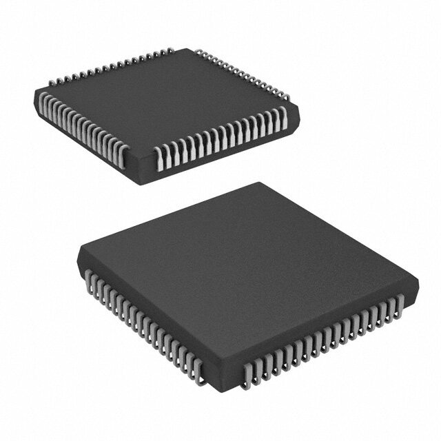
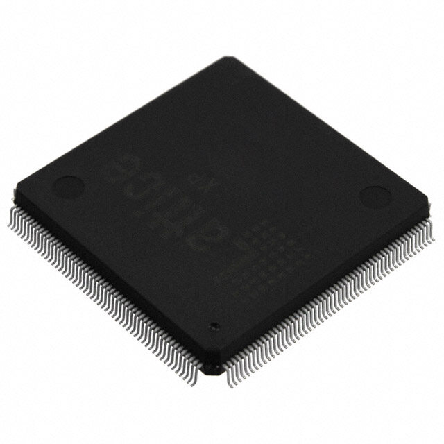
| 描述 | IC FPGA 171 I/O 208PQFP |
| 产品分类 | |
| I/O数 | 171 |
| LAB/CLB数 | 6036 |
| 品牌 | Microsemi SoC |
| 数据手册 | http://www.microsemi.com/index.php?option=com_docman&task=doc_download&gid=130722 |
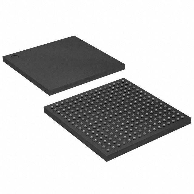
| 产品图片 |
|
| 产品型号 | A54SX72A-PQG208 |
| rohs | 无铅 / 符合限制有害物质指令(RoHS)规范要求 |
| 产品系列 | SX-A |
| 供应商器件封装 | 208-PQFP(28x28) |
| 其它名称 | 1100-1074 |
| 安装类型 | 表面贴装 |
| 封装/外壳 | 208-BFQFP |
| 工作温度 | 0°C ~ 70°C |
| 总RAM位数 | - |
| 栅极数 | 108000 |
| 标准包装 | 24 |
| 电压-电源 | 2.25 V ~ 5.25 V |
| 逻辑元件/单元数 | - |


- 商务部:美国ITC正式对集成电路等产品启动337调查
- 曝三星4nm工艺存在良率问题 高通将骁龙8 Gen1或转产台积电
- 太阳诱电将投资9.5亿元在常州建新厂生产MLCC 预计2023年完工
- 英特尔发布欧洲新工厂建设计划 深化IDM 2.0 战略
- 台积电先进制程称霸业界 有大客户加持明年业绩稳了
- 达到5530亿美元!SIA预计今年全球半导体销售额将创下新高
- 英特尔拟将自动驾驶子公司Mobileye上市 估值或超500亿美元
- 三星加码芯片和SET,合并消费电子和移动部门,撤换高东真等 CEO
- 三星电子宣布重大人事变动 还合并消费电子和移动部门
- 海关总署:前11个月进口集成电路产品价值2.52万亿元 增长14.8%

PDF Datasheet 数据手册内容提取
v5.3 SX-A Family FPGAs ™ ue Leading-Edge Performance (cid:129) Configurable I/O Support for 3.3V/5V PCI, 5V TTL, 3.3 VLVTTL, 2.5 V LVCMOS2 • 250 MHz System Performance (cid:129) 2.5 V, 3.3 V, and 5 V Mixed-Voltage Operation with (cid:129) 350 MHz Internal Performance 5V Input Tolerance and 5 V Drive Strength (cid:129) Devices Support Multiple Temperature Grades Specifications (cid:129) Configurable Weak-Resistor Pull-Up or Pull-Down for I/O at Power-Up (cid:129) 12,000 to 108,000 Available System Gates (cid:129) Individual Output Slew Rate Control (cid:129) Up to 360 User-Programmable I/O Pins (cid:129) Up to 100% Resource Utilization and 100% Pin (cid:129) Up to 2,012 Dedicated Flip-Flops Locking (cid:129) 0.22 μ / 0.25 μ CMOS Process Technology (cid:129) Deterministic, User-Controllable Timing (cid:129) Unique In-System Diagnostic and Verification Capability with Silicon Explorer II Features (cid:129) Boundary-Scan Testing in Compliance with IEEE Standard1149.1 (JTAG) (cid:129) Hot-Swap Compliant I/Os (cid:129) Actel Secure Programming Technology with (cid:129) Power-Up/Down Friendly (No Sequencing Required FuseLock™ Prevents Reverse Engineering and for Supply Voltages) Design Theft (cid:129) 66 MHz PCI Compliant (cid:129) Nonvolatile, Single-Chip Solution Table 1 • SX-A Product Profile Device A54SX08A A54SX16A A54SX32A A54SX72A Capacity Typical Gates 8,000 16,000 32,000 72,000 System Gates 12,000 24,000 48,000 108,000 Logic Modules 768 1,452 2,880 6,036 Combinatorial Cells 512 924 1,800 4,024 Dedicated Flip-Flops 256 528 1,080 2,012 Maximum Flip-Flops 512 1 990 1,980 4,024 Maximum User I/Os 130 180 249 360 Global Clocks 3 3 3 3 Quadrant Clocks 0 0 0 4 Boundary Scan Testing Yes Yes Yes Yes 3.3 V / 5 V PCI Yes Yes Yes Yes Input Set-Up (External) 0 ns 0 ns 0 ns 0 ns Speed Grades2 –F, Std, –1, –2 –F, Std, –1, –2, –3 –F, Std, –1, –2, –3 –F, Std, –1, –2, –3 Temperature Grades C, I, A, M C, I, A, M C, I, A, M C, I, A, M Package (by pin count) PQFP 208 208 208 208 TQFP 100, 144 100, 144 100, 144, 176 – PBGA – – 329 – FBGA 144 144, 256 144, 256, 484 256, 484 CQFP – – 208, 256 208, 256 Notes: 1. A maximum of 512 registers is possible if all 512 C cells are used to build an additional 256 registers. 2. All –3 speed grades have been discontinued. February 2007 i © 2007 Actel Corporation See the Actel website for the latest version of the datasheet.
SX-A Family FPGAs Ordering Information A54SX16A 2 PQ G 208 Application (Temperature Range) Blank = Commercial (0 to +70°) I = Industrial (-40 to +85°C) A = Automotive (-40 to +125°C) M = Military (-55 to +125°C) B = MIL-STD-883 Class B Package Lead Count Lead-Free Packaging Blank = Standard Packaging G = RoHS Compliant Packaging Package Type BG = 1.27 mm Plastic Ball Grid Array FG = 1.0 mm Fine Pitch Ball Grid Array PQ = Plastic Quad Flat Pack TQ = Thin (1.4 mm) Quad Flat Pack CQ = Ceramic Quad Flat Pack1 Speed Grade Blank = Standard Speed –1 = Approximately 15% Faster than Standard –2 = Approximately 25% Faster than Standard –3 = Approximately 35% Faster than Standard2 –F = Approximately 40% Slower than Standard Part Number A54SX08A = 12,000 System Gates A54SX16A = 24,000 System Gates A54SX32A = 48,000 System Gates A54SX72A = 108,000 System Gates Notes: 1. For more information about the CQFP package options, refer to the HiRel SX-A datasheet. 2. All –3 speed grades have been discontinued. Device Resources User I/Os (Including Clock Buffers) 208-Pin 100-Pin 144-Pin 176-Pin 329-Pin 144-Pin 256-Pin 484-Pin Device PQFP TQFP TQFP TQFP PBGA FBGA FBGA FBGA A54SX08A 130 81 113 – – 111 – – A54SX16A 175 81 113 – – 111 180 – A54SX32A 174 81 113 147 249 111 203 249 A54SX72A 171 – – – – – 203 360 Notes:Package Definitions: PQFP = Plastic Quad Flat Pack, TQFP = Thin Quad Flat Pack, PBGA = Plastic Ball Grid Array, FBGA = Fine Pitch Ball GridArray ii v5.3
SX-A Family FPGAs Temperature Grade Offering Package A54SX08A A54SX16A A54SX32A A54SX72A PQ208 C,I,A,M C,I,A,M C,I,A,M C,I,A,M TQ100 C,I,A,M C,I,A,M C,I,A,M TQ144 C,I,A,M C,I,A,M C,I,A,M TQ176 C,I,M BG329 C,I,M FG144 C,I,A,M C,I,A,M C,I,A,M FG256 C,I,A,M C,I,A,M C,I,A,M FG484 C,I,M C,I,A,M CQ208 C,M,B C,M,B CQ256 C,M,B C,M,B Notes: 1. C = Commercial 2. I = Industrial 3. A = Automotive 4. M = Military 5. B = MIL-STD-883 Class B 6. For more information regarding automotive products, refer to the SX-A Automotive Family FPGAs datasheet. 7. For more information regarding Mil-Temp and ceramic packages, refer to the HiRel SX-A Family FPGAs datasheet. Speed Grade and Temperature Grade Matrix F Std –1 –2 –3 Commercial ✓ ✓ ✓ ✓ Discontinued Industrial ✓ ✓ ✓ Discontinued Automotive ✓ Military ✓ ✓ MIL-STD-883B ✓ ✓ Notes: 1. For more information regarding automotive products, refer to the SX-A Automotive Family FPGAs datasheet. 2. For more information regarding Mil-Temp and ceramic packages, refer to the HiRel SX-A Family FPGAs datasheet. Contact your Actel Sales representative for more information on availability. v5.3 iii
SX-A Family FPGAs Table of Contents General Description Introduction . . . . . . . . . . . . . . . . . . . . . . . . . . . . . . . . . . . . . . . . . . . . . . . . . . . . . . . . 1-1 SX-A Family Architecture . . . . . . . . . . . . . . . . . . . . . . . . . . . . . . . . . . . . . . . . . . . . . . 1-1 Other Architectural Features . . . . . . . . . . . . . . . . . . . . . . . . . . . . . . . . . . . . . . . . . . . 1-7 Programming . . . . . . . . . . . . . . . . . . . . . . . . . . . . . . . . . . . . . . . . . . . . . . . . . . . . . . 1-13 Related Documents . . . . . . . . . . . . . . . . . . . . . . . . . . . . . . . . . . . . . . . . . . . . . . . . . 1-14 Pin Description . . . . . . . . . . . . . . . . . . . . . . . . . . . . . . . . . . . . . . . . . . . . . . . . . . . . . 1-15 Detailed Specifications Operating Conditions . . . . . . . . . . . . . . . . . . . . . . . . . . . . . . . . . . . . . . . . . . . . . . 2-1 Typical SX-A Standby Current . . . . . . . . . . . . . . . . . . . . . . . . . . . . . . . . . . . . . . . . . 2-1 Electrical Specifications . . . . . . . . . . . . . . . . . . . . . . . . . . . . . . . . . . . . . . . . . . . . . 2-2 PCI Compliance for the SX-A Family . . . . . . . . . . . . . . . . . . . . . . . . . . . . . . . . . . . . . 2-3 Thermal Characteristics . . . . . . . . . . . . . . . . . . . . . . . . . . . . . . . . . . . . . . . . . . . . . . 2-11 SX-A Timing Model . . . . . . . . . . . . . . . . . . . . . . . . . . . . . . . . . . . . . . . . . . . . . . . . . . 2-14 Sample Path Calculations . . . . . . . . . . . . . . . . . . . . . . . . . . . . . . . . . . . . . . . . . . . . . 2-14 Output Buffer Delays . . . . . . . . . . . . . . . . . . . . . . . . . . . . . . . . . . . . . . . . . . . . . . . . 2-15 AC Test Loads . . . . . . . . . . . . . . . . . . . . . . . . . . . . . . . . . . . . . . . . . . . . . . . . . . . . . . 2-15 Input Buffer Delays . . . . . . . . . . . . . . . . . . . . . . . . . . . . . . . . . . . . . . . . . . . . . . . . . . 2-16 C-Cell Delays . . . . . . . . . . . . . . . . . . . . . . . . . . . . . . . . . . . . . . . . . . . . . . . . . . . . . . . 2-16 Cell Timing Characteristics . . . . . . . . . . . . . . . . . . . . . . . . . . . . . . . . . . . . . . . . . . . . 2-16 Timing Characteristics . . . . . . . . . . . . . . . . . . . . . . . . . . . . . . . . . . . . . . . . . . . . . . . 2-17 Temperature and Voltage Derating Factors . . . . . . . . . . . . . . . . . . . . . . . . . . . . . . 2-17 Timing Characteristics . . . . . . . . . . . . . . . . . . . . . . . . . . . . . . . . . . . . . . . . . . . . . . . 2-18 Package Pin Assignments 208-Pin PQFP . . . . . . . . . . . . . . . . . . . . . . . . . . . . . . . . . . . . . . . . . . . . . . . . . . . . . . . . 3-1 100-Pin TQFP . . . . . . . . . . . . . . . . . . . . . . . . . . . . . . . . . . . . . . . . . . . . . . . . . . . . . . . 3-5 144-Pin TQFP . . . . . . . . . . . . . . . . . . . . . . . . . . . . . . . . . . . . . . . . . . . . . . . . . . . . . . . . 3-8 176-Pin TQFP . . . . . . . . . . . . . . . . . . . . . . . . . . . . . . . . . . . . . . . . . . . . . . . . . . . . . . . 3-11 329-Pin PBGA . . . . . . . . . . . . . . . . . . . . . . . . . . . . . . . . . . . . . . . . . . . . . . . . . . . . . . 3-14 144-Pin FBGA . . . . . . . . . . . . . . . . . . . . . . . . . . . . . . . . . . . . . . . . . . . . . . . . . . . . . . 3-18 256-Pin FBGA . . . . . . . . . . . . . . . . . . . . . . . . . . . . . . . . . . . . . . . . . . . . . . . . . . . . . . 3-21 484-Pin FBGA . . . . . . . . . . . . . . . . . . . . . . . . . . . . . . . . . . . . . . . . . . . . . . . . . . . . . . 3-26 Datasheet Information List of Changes . . . . . . . . . . . . . . . . . . . . . . . . . . . . . . . . . . . . . . . . . . . . . . . . . . . . . . 4-1 Datasheet Categories . . . . . . . . . . . . . . . . . . . . . . . . . . . . . . . . . . . . . . . . . . . . . . . . . 4-3 International Traffic in Arms Regulations (ITAR) and Export Administration Regulations (EAR) . . . . . . . . . . . . . . . . . . . . . . . . . . . . . . . . . . . . . . . . . . . . . . . . . . . . 4-3 iv v5.3
SX-A Family FPGAs General Description Introduction SX-A Family Architecture The Actel SX-A family of FPGAs offers a cost-effective, The SX-A family’s device architecture provides a unique single-chip solution for low-power, high-performance approach to module organization and chip routing that designs. Fabricated on 0.22 μm / 0.25 μm CMOS satisfies performance requirements and delivers the most antifuse technology and with the support of 2.5 V, optimal register/logic mix for a wide variety of 3.3 V and 5 V I/Os, the SX-A is a versatile platform to applications. integrate designs while significantly reducing time- Interconnection between these logic modules is achieved to-market. using Actel’s patented metal-to-metal programmable antifuse interconnect elements (Figure1-1). The antifuses are normally open circuit and, when programmed, form a permanent low-impedance connection. Routing Tracks Amorphous Silicon/ Dielectric Antifuse Tungsten Plug Via Metal 4 Metal 3 Tungsten Plug Via Metal 2 Metal 1 Tungsten Plug Contact Silicon Substrate Note: The A54SX72A device has four layers of metal with the antifuse between Metal 3 and Metal 4. The A54SX08A, A54SX16A, and A54SX32A devices have three layers of metal with the antifuse between Metal 2 and Metal 3. Figure 1-1 (cid:129) SX-A Family Interconnect Elements v5.3 1-1
SX-A Family FPGAs Logic Module Design different combinatorial functions to be implemented in a single module. An example of the flexibility enabled by The SX-A family architecture is described as a “sea-of- the inversion capability is the ability to integrate a 3-input modules” architecture because the entire floor of the exclusive-OR function into a single C-cell. This facilitates device is covered with a grid of logic modules with construction of 9-bit parity-tree functions with 1.9 ns virtually no chip area lost to interconnect elements or propagation delays. routing. The Actel SX-A family provides two types of logic modules: the register cell (R-cell) and the Module Organization combinatorial cell (C-cell). The R-cell contains a flip-flop featuring asynchronous clear, All C-cell and R-cell logic modules are arranged into asynchronous preset, and clock enable, using the S0 and S1 horizontal banks called Clusters. There are two types of lines control signals (Figure1-2). The R-cell registers feature Clusters: Type 1 contains two C-cells and one R-cell, while programmable clock polarity selectable on a register-by- Type 2 contains one C-cell and two R-cells. register basis. This provides additional flexibility while Clusters are grouped together into SuperClusters allowing mapping of synthesized functions into the SX-A (Figure1-4 on page 1-3). SuperCluster 1 is a two-wide FPGA. The clock source for the R-cell can be chosen from grouping of Type 1 Clusters. SuperCluster 2 is a two-wide either the hardwired clock, the routed clocks, or internal group containing one Type 1 Cluster and one Type 2 Cluster. SX-A devices feature more SuperCluster 1 logic. modules than SuperCluster 2 modules because designers The C-cell implements a range of combinatorial functions typically require significantly more combinatorial logic of up to five inputs (Figure1-3). Inclusion of the DB input than flip-flops. and its associated inverter function allows up to 4,000 Routed Data Input S1 S0 PRE DirectConnect D Q Y Input HCLK CLKA, CLR CLKB, Internal Logic CKS CKP Figure 1-2 (cid:129) R-Cell D0 D1 Y D2 D3 Sa Sb DB A0 B0 A1 B1 Figure 1-3 (cid:129) C-Cell 1-2 v5.3
SX-A Family FPGAs Routing Resources The routing and interconnect resources of SX-A devices interconnection to achieve its fast signal propagation are in the top two metal layers above the logic modules time of less than 0.1 ns. (Figure1-1 on page 1-1), providing optimal use of silicon, FastConnect enables horizontal routing between any thus enabling the entire floor of the device to be two logic modules within a given SuperCluster, and spanned with an uninterrupted grid of logic modules. vertical routing with the SuperCluster immediately Interconnection between these logic modules is achieved below it. Only one programmable connection is used in a using the Actel patented metal-to-metal programmable FastConnect path, delivering a maximum pin-to-pin propagation time of 0.3 ns. antifuse interconnect elements. The antifuses are normally open circuits and, when programmed, form a In addition to DirectConnect and FastConnect, the permanent low-impedance connection. architecture makes use of two globally oriented routing resources known as segmented routing and high-drive Clusters and SuperClusters can be connected through the routing. The Actel segmented routing structure provides use of two innovative local routing resources called a variety of track lengths for extremely fast routing FastConnect and DirectConnect, which enable extremely between SuperClusters. The exact combination of track fast and predictable interconnection of modules within lengths and antifuses within each path is chosen by the Clusters and SuperClusters (Figure1-5 on page 1-4 and 100% automatic place-and-route software to minimize Figure1-6 on page 1-4). This routing architecture also signal propagation delays. dramatically reduces the number of antifuses required to The general system of routing tracks allows any logic complete a circuit, ensuring the highest possible module in the array to be connected to any other logic performance, which is often required in applications such or I/O module. Within this system, most connections as fast counters, state machines, and data path logic. The typically require three or fewer antifuses, resulting in interconnect elements (i.e., the antifuses and metal fast and predictable performance. tracks) have lower capacitance and lower resistance than The unique local and general routing structure featured any other device of similar capacity, leading to the fastest in SX-A devices allows 100% pin-locking with full logic signal propagation in the industry. utilization, enables concurrent printed circuit board DirectConnect is a horizontal routing resource that (PCB) development, reduces design time, and allows provides connections from a C-cell to its neighboring designers to achieve performance goals with minimum R-Cell in a given SuperCluster. DirectConnect uses a effort. hardwired signal path requiring no programmable R-Cell C-Cell Routed D0 S1 S0 Data Input D1 PRE Y D2 DirectConnect Input D Q Y D3 Sa Sb HCLK CLKA, CLR CLKB, DB Internal Logic CKS CKP A0 B0 A1 B1 Cluster 1 Cluster 1 Cluster 2 Cluster 1 Type 1 SuperCluster Type 2 SuperCluster Figure 1-4 (cid:129) Cluster Organization v5.3 1-3
SX-A Family FPGAs DirectConnect (cid:129) No Antifuses (cid:129) 0.1 ns Maximum Routing Delay FastConnect (cid:129) One Antifuse (cid:129) 0.3 ns Maximum Routing Delay Routing Segments (cid:129) Typically Two Antifuses (cid:129) Max. Five Antifuses Figure 1-5 (cid:129) DirectConnect and FastConnect for Type 1 SuperClusters DirectConnect (cid:129) No Antifuses (cid:129) 0.1 ns Maximum Routing Delay FastConnect (cid:129) One Antifuse (cid:129) 0.3 ns Maximum Routing Delay Routing Segments (cid:129) Typically Two Antifuses (cid:129) Max. Five Antifuses Figure 1-6 (cid:129) DirectConnect and FastConnect for Type 2 SuperClusters 1-4 v5.3
SX-A Family FPGAs Clock Resources Actel’s high-drive routing structure provides three clock and CLKB circuit used and the macros supported in SX-A networks (Table1-1). The first clock, called HCLK, is devices with the exception of A54SX72A. hardwired from the HCLK buffer to the clock select In addition, the A54SX72A device provides four multiplexor (MUX) in each R-cell. HCLK cannot be quadrant clocks (QCLKA, QCLKB, QCLKC, and QCLKD— connected to combinatorial logic. This provides a fast corresponding to bottom-left, bottom-right, top-left, propagation path for the clock signal. If not used, this and top-right locations on the die, respectively), which pin must be set as Low or High on the board. It must not can be sourced from external pins or from internal logic be left floating. Figure1-7 describes the clock circuit signals within the device. Each of these clocks can used for the constant load HCLK and the macros individually drive up to an entire quadrant of the chip, or they can be grouped together to drive multiple supported. quadrants (Figure1-9 on page 1-6). QCLK pins can HCLK does not function until the fourth clock cycle each function as user I/O pins. If not used, the QCLK pins time the device is powered up to prevent false output must be tied Low or High on the board and must not be levels due to any possible slow power-on-reset signal and left floating. fast start-up clock circuit. To activate HCLK from the first For more information on how to use quadrant clocks in cycle, the TRST pin must be reserved in the Design the A54SX72A device, refer to the Global Clock Networks software and the pin must be tied to GND on the board. in Actel’s Antifuse Devices and Using A54SX72A and Two additional clocks (CLKA, CLKB) are global clocks that RT54SX72S Quadrant Clocks application notes. can be sourced from external pins or from internal logic The CLKA, CLKB, and QCLK circuits for A54SX72A as well signals within the SX-A device. CLKA and CLKB may be as the macros supported are shown in Figure1-10 on connected to sequential cells or to combinational logic. If page 1-6. Note that bidirectional clock buffers are only CLKA or CLKB pins are not used or sourced from signals, available in A54SX72A. For more information, refer to these pins must be set as Low or High on the board. They the "Pin Description" section on page1-15. must not be left floating. Figure1-8 describes the CLKA Table 1-1 (cid:129) SX-A Clock Resources A54SX08A A54SX16A A54SX32A A54SX72A Routed Clocks (CLKA, CLKB) 2 2 2 2 Hardwired Clocks (HCLK) 1 1 1 1 Quadrant Clocks (QCLKA, QCLKB, QCLKC, QCLKD) 0 0 0 4 Constant Load Clock Network HCLKBUF Figure 1-7 (cid:129) SX-A HCLK Clock Buffer Clock Network From Internal Logic CLKBUF CLKBUFI CLKINT CLKINTI Figure 1-8 (cid:129) SX-A Routed Clock Buffer v5.3 1-5
SX-A Family FPGAs 4 QCLKBUFS 4 Quadrant 2 5:1 5:1 Quadrant 3 QCLKINT (to array) QCLKINT (to array) 4 Quadrant 0 5:1 5:1 Quadrant 1 QCLKINT (to array) QCLKINT (to array) Figure 1-9 (cid:129) SX-A QCLK Architecture OE From Internal Logic Clock Network From Internal Logic CLKBUF QCLKBUF CLKBUFI QCLKBUFI CLKINT QCLKINT CLKINTI QCLKINTI CLKBIBUF QCLKBIBUF CLKBIBUFI QCLKBIBUFI Figure 1-10 (cid:129) A54SX72A Routed Clock and QCLK Buffer 1-6 v5.3
SX-A Family FPGAs Other Architectural Features I/O Modules For a simplified I/O schematic, refer to Figure 1 in the application note, Actel eX, SX-A, and RTSX-S I/Os. Technology Each user I/O on an SX-A device can be configured as an The Actel SX-A family is implemented on a high-voltage, input, an output, a tristate output, or a bidirectional pin. twin-well CMOS process using 0.22μ/0.25μ design Mixed I/O standards can be set for individual pins, rules. The metal-to-metal antifuse is comprised of a though this is only allowed with the same voltage as the combination of amorphous silicon and dielectric material input. These I/Os, combined with array registers, can with barrier metals and has a programmed ('on' state) achieve clock-to-output-pad timing as fast as 3.8 ns, even resistance of 25 Ω with capacitance of 1.0 fF for low without the dedicated I/O registers. In most FPGAs, I/O signal impedance. cells that have embedded latches and flip-flops, requiring instantiation in HDL code; this is a design Performance complication not encountered in SX-A FPGAs. Fast pin- The unique architectural features of the SX-A family to-pin timing ensures that the device is able to interface enable the devices to operate with internal clock with any other device in the system, which in turn frequencies of 350MHz, causing very fast execution of enables parallel design of system components and even complex logic functions. The SX-A family is an reduces overall design time. All unused I/Os are optimal platform upon which to integrate the configured as tristate outputs by the Actel Designer functionality previously contained in multiple complex software, for maximum flexibility when designing new programmable logic devices (CPLDs). In addition, designs boards or migrating existing designs. that previously would have required a gate array to meet SX-A I/Os should be driven by high-speed push-pull performance goals can be integrated into an SX-A device devices with a low-resistance pull-up device when being with dramatic improvements in cost and time-to-market. configured as tristate output buffers. If the I/O is driven Using timing-driven place-and-route tools, designers can by a voltage level greater than V and a fast push-pull CCI achieve highly deterministic device performance. device is NOT used, the high-resistance pull-up of the driver and the internal circuitry of the SX-A I/O may User Security create a voltage divider. This voltage divider could pull the input voltage below specification for some devices Reverse engineering is virtually impossible in SX-A connected to the driver. A logic '1' may not be correctly devices because it is extremely difficult to distinguish presented in this case. For example, if an open drain between programmed and unprogrammed antifuses. In driver is used with a pull-up resistor to 5 V to provide the addition, since SX-A is a nonvolatile, single-chip solution, logic '1' input, and V is set to 3.3 V on the SX-A device, there is no configuration bitstream to intercept at device CCI the input signal may be pulled down by the SX-A input. power-up. Each I/O module has an available power-up resistor of The Actel FuseLock advantage ensures that unauthorized approximately 50 kΩ that can configure the I/O in a users will not be able to read back the contents of an known state during power-up. For nominal pull-up and Actel antifuse FPGA. In addition to the inherent pull-down resistor values, refer to Table1-4 on page1-8 strengths of the architecture, special security fuses that of the application note Actel eX, SX-A, and RTSX-S I/Os. prevent internal probing and overwriting are hidden Just slightly before V reaches 2.5 V, the resistors are throughout the fabric of the device. They are located CCA disabled, so the I/Os will be controlled by user logic. See where they cannot be accessed or bypassed without Table1-2 on page1-8 and Table1-3 on page1-8 for destroying access to the rest of the device, making both more information concerning available I/O features. invasive and more-subtle noninvasive attacks ineffective against Actel antifuse FPGAs. Look for this symbol to ensure your valuable IP is secure (Figure1-11). ™ u e Figure 1-11 (cid:129) FuseLock For more information, refer to Actel’s Implementation of Security in Actel Antifuse FPGAs application note. v5.3 1-7
SX-A Family FPGAs Power-Up/Down and Hot Swapping SX-A I/Os are configured to be hot-swappable, with the are reached. Table1-4 summarizes the V voltage at CCA exception of 3.3 V PCI. During power-up/down (or partial which the I/Os behave according to the user’s design for up/down), all I/Os are tristated. V and V do not an SX-A device at room temperature for various ramp-up CCA CCI have to be stable during power-up/down, and can be rates. The data reported assumes a linear ramp-up powered up/down in any order. When the SX-A device is profile to 2.5 V. For more information on power-up and plugged into an electrically active system, the device will hot-swapping, refer to the application note, Actel SX-A not degrade the reliability of or cause damage to the and RT54SX-S Devices in Hot-Swap and Cold-Sparing host system. The device’s output pins are driven to a high Applications. impedance state until normal chip operating conditions Table 1-2 (cid:129) I/O Features Function Description Input Buffer Threshold Selections (cid:129) 5 V: PCI, TTL (cid:129) 3.3 V: PCI, LVTTL (cid:129) 2.5 V: LVCMOS2 (commercial only) Flexible Output Driver (cid:129) 5 V: PCI, TTL (cid:129) 3.3 V: PCI, LVTTL (cid:129) 2.5 V: LVCMOS2 (commercial only) Output Buffer “Hot-Swap” Capability (3.3 V PCI is not hot swappable) (cid:129) I/O on an unpowered device does not sink current (cid:129) Can be used for “cold-sparing” Selectable on an individual I/O basis Individually selectable slew rate; high slew or low slew (The default is high slew rate). The slew is only affected on the falling edge of an output. Rising edges of outputs are not affected. Power-Up Individually selectable pull-ups and pull-downs during power-up (default is to power-up in tristate) Enables deterministic power-up of device V and V can be powered in any order CCA CCI Table 1-3 (cid:129) I/O Characteristics for All I/O Configurations Hot Swappable Slew Rate Control Power-Up Resistor TTL, LVTTL, LVCMOS2 Yes Yes. Only affects falling edges of outputs Pull-up or pull-down 3.3 V PCI No No. High slew rate only Pull-up or pull-down 5 V PCI Yes No. High slew rate only Pull-up or pull-down Table 1-4 (cid:129) Power-Up Time at which I/Os Become Active Supply Ramp Rate 0.25 V/μs 0.025 V/μs 5 V/ms 2.5 V/ms 0.5 V/ms 0.25 V/ms 0.1 V/ms 0.025 V/ms Units μs μs ms ms ms ms ms ms A54SX08A 10 96 0.34 0.65 2.7 5.4 12.9 50.8 A54SX16A 10 100 0.36 0.62 2.5 4.7 11.0 41.6 A54SX32A 10 100 0.46 0.74 2.8 5.2 12.1 47.2 A54SX72A 10 100 0.41 0.67 2.6 5.0 12.1 47.2 1-8 v5.3
SX-A Family FPGAs Boundary-Scan Testing (BST) Flexible Mode In Flexible mode, TDI, TCK, and TDO may be employed as All SX-A devices are IEEE 1149.1 compliant and offer either user I/Os or as JTAG input pins. The internal superior diagnostic and testing capabilities by providing resistors on the TMS and TDI pins are not present in Boundary Scan Testing (BST) and probing capabilities. flexible JTAG mode. The BST function is controlled through the special JTAG pins (TMS, TDI, TCK, TDO, and TRST). The functionality of To select the Flexible mode, uncheck the Reserve JTAG the JTAG pins is defined by two available modes: box in the Device Selection Wizard dialog in the Actel Dedicated and Flexible. TMS cannot be employed as a Designer software. In Flexible mode, TDI, TCK, and TDO user I/O in either mode. pins may function as user I/Os or BST pins. The functionality is controlled by the BST Test Access Port Dedicated Mode (TAP) controller. The TAP controller receives two control inputs, TMS and TCK. Upon power-up, the TAP controller In Dedicated mode, all JTAG pins are reserved for BST; designers cannot use them as regular I/Os. An internal enters the Test-Logic-Reset state. In this state, TDI, TCK, pull-up resistor is automatically enabled on both TMS and TDO function as user I/Os. The TDI, TCK, and TDO are and TDI pins, and the TMS pin will function as defined in transformed from user I/Os into BST pins when a rising the IEEE 1149.1 (JTAG) specification. edge on TCK is detected while TMS is at logic low. To return to Test-Logic Reset state, TMS must be high for at To select Dedicated mode, the user must reserve the least five TCK cycles. An external 10 k pull-up resistor JTAG pins in Actel’s Designer software. Reserve the JTAG to V should be placed on the TMS pin to pull it pins by checking the Reserve JTAG box in the Device CCI High by default. Selection Wizard (Figure1-12). Table1-6 describes the different configuration The default for the software is Flexible mode; all boxes requirements of BST pins and their functionality in are unchecked. Table1-5 lists the definitions of the different modes. options in the Device Selection Wizard. Table 1-6 (cid:129) Boundary-Scan Pin Configurations and Functions Designer "Reserve JTAG" TAP Controller Mode Selection State Dedicated (JTAG) Checked Any Flexible (User I/O) Unchecked Test-Logic-Reset Flexible (JTAG) Unchecked Any EXCEPT Test- Logic-Reset TRST Pin Figure 1-12 (cid:129) Device Selection Wizard The TRST pin functions as a dedicated Boundary-Scan Table 1-5 (cid:129) Reserve Pin Definitions Reset pin when the Reserve JTAG Test Reset option is selected as shown in Figure1-12. An internal pull-up Pin Function resistor is permanently enabled on the TRST pin in this Reserve JTAG Keeps pins from being used and mode. Actel recommends connecting this pin to ground changes the behavior of JTAG pins (no in normal operation to keep the JTAG state controller in pull-up on TMS) the Test-Logic-Reset state. When JTAG is being used, it can be left floating or can be driven high. Reserve JTAG Test Regular I/O or JTAG reset with an Reset internal pull-up When the Reserve JTAG Test Reset option is not selected, this pin will function as a regular I/O. If unused Reserve Probe Keeps pins from being used or regular as an I/O in the design, it will be configured as a tristated I/O output. v5.3 1-9
SX-A Family FPGAs JTAG Instructions Table1-7 lists the supported instructions with the corresponding IR codes for SX-A devices. Table1-8 lists the codes returned after executing the IDCODE instruction for SX-A devices. Note that bit 0 is always '1'. Bits 11-1 are always '02F', which is the Actel manufacturer code. Table 1-7 (cid:129) JTAG Instruction Code Instructions (IR4:IR0) Binary Code EXTEST 00000 SAMPLE/PRELOAD 00001 INTEST 00010 USERCODE 00011 IDCODE 00100 HighZ 01110 CLAMP 01111 Diagnostic 10000 BYPASS 11111 Reserved All others Table 1-8 (cid:129) JTAG Instruction Code Device Process Revision Bits 31-28 Bits 27-12 A54SX08A 0.22 µ 0 8, 9 40B4, 42B4 1 A, B 40B4, 42B4 A54SX16A 0.22 µ 0 9 40B8, 42B8 1 B 40B8, 42B8 0.25 µ 1 B 22B8 A54SX32A 0.2 2µ 0 9 40BD, 42BD 1 B 40BD, 42BD 0.25 µ 1 B 22BD A54SX72A 0.22 µ 0 9 40B2, 42B2 1 B 40B2, 42B2 0.25 µ 1 B 22B2 1-10 v5.3
SX-A Family FPGAs Probing Capabilities SX-A devices also provide an internal probing capability When selecting the Reserve Probe Pin box as shown in that is accessed with the JTAG pins. The Silicon Explorer II Figure1-12 on page 1-9, direct the layout tool to reserve diagnostic hardware is used to control the TDI, TCK, TMS, the PRA and PRB pins as dedicated outputs for probing. and TDO pins to select the desired nets for debugging. This Reserve option is merely a guideline. If the designer The user assigns the selected internal nets in Actel Silicon assigns user I/Os to the PRA and PRB pins and selects the Explorer II software to the PRA/PRB output pins for Reserve Probe Pin option, Designer Layout will observation. Silicon Explorer II automatically places the override the Reserve Probe Pin option and place the device into JTAG mode. However, probing functionality is user I/Os on those pins. only activated when the TRST pin is driven high or left To allow probing capabilities, the security fuse must not floating, allowing the internal pull-up resistor to pull be programmed. Programming the security fuse disables TRST High. If the TRST pin is held Low, the TAP controller the JTAG and probe circuitry. Table1-9 summarizes the remains in the Test-Logic-Reset state so no probing can possible device configurations for probing once the be performed. However, the user must drive the TRST pin device leaves the Test-Logic-Reset JTAG state. High or allow the internal pull-up resistor to pull TRST High. Table 1-9 (cid:129) Device Configuration Options for Probe Capability (TRST Pin Reserved) JTAG Mode TRST1 Security Fuse Programmed PRA, PRB2 TDI, TCK, TDO2 Dedicated Low No User I/O3 JTAG Disabled High No Probe Circuit Outputs JTAG I/O Flexible Low No User I/O3 User I/O3 High No Probe Circuit Outputs JTAG I/O Yes Probe Circuit Secured Probe Circuit Secured Notes: 1. If the TRST pin is not reserved, the device behaves according to TRST = High as described in the table. 2. Avoid using the TDI, TCK, TDO, PRA, and PRB pins as input or bidirectional ports. Since these pins are active during probing, input signals will not pass through these pins and may cause contention. 3. If no user signal is assigned to these pins, they will behave as unused I/Os in this mode. Unused pins are automatically tristated by the Designer software. v5.3 1-11
SX-A Family FPGAs SX-A Probe Circuit Control Pins PRA/PRB pins for observation. Figure1-13 illustrates the interconnection between Silicon ExplorerII and the FPGA SX-A devices contain internal probing circuitry that to perform in-circuit verification. provides built-in access to every node in a design, enabling 100% real-time observation and analysis of a device's internal logic nodes without design iteration. Design Considerations The probe circuitry is accessed by Silicon ExplorerII, an In order to preserve device probing capabilities, users easy to use, integrated verification and logic analysis tool should avoid using the TDI, TCK, TDO, PRA, and PRB pins that can sample data at 100MHz (asynchronous) or as input or bidirectional ports. Since these pins are active 66MHz (synchronous). SiliconExplorerII attaches to a during probing, critical input signals through these pins PC’s standard COM port, turning the PC into a fully functional 18-channel logic analyzer. SiliconExplorerII are not available. In addition, the security fuse must not be programmed to preserve probing capabilities. Actel allows designers to complete the design verification process at their desks and reduces verification time from recommends that you use a 70Ω series termination resistor on every probe connector (TDI, TCK, TMS, TDO, several hours per cycle to a few seconds. PRA, PRB). The 70Ω series termination is used to prevent The Silicon Explorer II tool uses the boundary-scan ports data transmission corruption during probing and (TDI, TCK, TMS, and TDO) to select the desired nets for reading back the checksum. verification. The selected internal nets are assigned to the al onels 16 ditiann dh AC 70 Ω SX-A FPGA TDI 70 Ω TCK Silicon Explorer II 70 Ω Serial Connection TMS 70 Ω TDO 70 Ω PRA 70 Ω PRB Figure 1-13 (cid:129) Probe Setup 1-12 v5.3
SX-A Family FPGAs Design Environment Programming The SX-A family of FPGAs is fully supported by both Actel Device programming is supported through Silicon Libero® Integrated Design Environment (IDE) and Sculptor series of programmers. In particular, Silicon Designer FPGA development software. Actel LiberoIDE is Sculptor is compact, robust, single-site and multi-site a design management environment, seamlessly device programmer for the PC. integrating design tools while guiding the user through With standalone software, Silicon Sculptor allows the design flow, managing all design and log files, and concurrent programming of multiple units from the passing necessary design data among tools. Additionally, same PC, ensuring the fastest programming times Libero IDE allows users to integrate both schematic and possible. Each fuse is subsequently verified by Silicon HDL synthesis into a single flow and verify the entire Sculptor II to insure correct programming. In addition, design in a single environment. Libero IDE includes integrity tests ensure that no extra fuses are Synplify® for Actel from Synplicity®, ViewDraw® for programmed. Silicon Sculptor also provides extensive Actel from Mentor Graphics®, ModelSim® HDL Simulator hardware self-testing capability. from Mentor Graphics, WaveFormer Lite™ from SynaptiCAD™, and Designer software from Actel. Refer The procedure for programming an SX-A device using to the Libero IDE flow diagram for more information Silicon Sculptor is as follows: (located on the Actel website). 1. Load the .AFM file Actel Designer software is a place-and-route tool and 2. Select the device to be programmed provides a comprehensive suite of backend support tools 3. Begin programming for FPGA development. The Designer software includes When the design is ready to go to production, Actel timing-driven place-and-route, and a world-class offers device volume-programming services either integrated static timing analyzer and constraints editor. through distribution partners or via in-house With the Designer software, a user can select and lock programming from the factory. package pins while only minimally impacting the results of place-and-route. Additionally, the back-annotation For detailed information on programming, read the flow is compatible with all the major simulators and the following documents Programming Antifuse Devices and simulation results can be cross-probed with Silicon Silicon Sculptor User’s Guide. Explorer II, Actel’s integrated verification and logic analysis tool. Another tool included in the Designer software is the SmarGen core generator, which easily creates popular and commonly used logic functions for implementation in your schematic or HDL design. Actel's Designer software is compatible with the most popular FPGA design entry and verification tools from companies such as Mentor Graphics, Synplicity, Synopsys, and Cadence Design Systems. The Designer software is available for both the Windows and UNIX operating systems. v5.3 1-13
SX-A Family FPGAs Related Documents Application Notes Global Clock Networks in Actel’s Antifuse Devices http://www.actel.com/documents/GlobalClk_AN.pdf Using A54SX72A and RT54SX72S Quadrant Clocks http://www.actel.com/documents/QCLK_AN.pdf Implementation of Security in Actel Antifuse FPGAs http://www.actel.com/documents/Antifuse_Security_AN.pdf Actel eX, SX-A, and RTSX-S I/Os http://www.actel.com/documents/AntifuseIO_AN.pdf Actel SX-A and RT54SX-S Devices in Hot-Swap and Cold-Sparing Applications http://www.actel.com/documents/HotSwapColdSparing_AN.pdf Programming Antifuse Devices http://www.actel.com/documents/AntifuseProgram_AN.pdf Datasheets HiRel SX-A Family FPGAs http://www.actel.com/documents/HRSXA_DS.pdf SX-A Automotive Family FPGAs http://www.actel.com/documents/SXA_Auto_DS.pdf User’s Guides Silicon Sculptor User’s Guide http://www.actel.com/documents/SiliSculptII_Sculpt3_ug.pdf 1-14 v5.3
SX-A Family FPGAs Pin Description PRA/B, I/O Probe A/B The Probe pin is used to output data from any user- CLKA/B, I/O Clock A and B defined design node within the device. This independent These pins are clock inputs for clock distribution diagnostic pin can be used in conjunction with the other networks. Input levels are compatible with standard TTL, probe pin to allow real-time diagnostic output of any LVTTL, LVCMOS2, 3.3V PCI, or 5V PCI specifications. The signal path within the device. The Probe pin can be used clock input is buffered prior to clocking the R-cells. When as a user-defined I/O when verification has been not used, this pin must be tied Low or High (NOT left completed. The pin’s probe capabilities can be floating) on the board to avoid unwanted power permanently disabled to protect programmed design consumption. confidentiality. For A54SX72A, these pins can also be configured as user TCK, I/O Test Clock I/Os. When employed as user I/Os, these pins offer built- Test clock input for diagnostic probe and device in programmable pull-up or pull-down resistors active programming. In Flexible mode, TCK becomes active during power-up only. When not used, these pins must when the TMS pin is set Low (refer to Table1-6 on be tied Low or High (NOT left floating). page1-9). This pin functions as an I/O when the QCLKA/B/C/D, I/O Quadrant Clock A, B, C, and D boundary scan state machine reaches the "logic reset" state. These four pins are the quadrant clock inputs and are only used for A54SX72A with A, B, C, and D TDI, I/O Test Data Input corresponding to bottom-left, bottom-right, top-left, Serial input for boundary scan testing and diagnostic and top-right quadrants, respectively. They are clock probe. In Flexible mode, TDI is active when the TMS pin is inputs for clock distribution networks. Input levels are set Low (refer to Table1-6 on page1-9). This pin compatible with standard TTL, LVTTL, LVCMOS2, 3.3V functions as an I/O when the boundary scan state PCI, or 5V PCI specifications. Each of these clock inputs machine reaches the “logic reset” state. can drive up to a quarter of the chip, or they can be grouped together to drive multiple quadrants. The clock TDO, I/O Test Data Output input is buffered prior to clocking the R-cells. When not Serial output for boundary scan testing. In flexible mode, used, these pins must be tied Low or High on the board TDO is active when the TMS pin is set Low (refer to (NOT left floating). Table1-6 on page1-9). This pin functions as an I/O when These pins can also be configured as user I/Os. When the boundary scan state machine reaches the "logic employed as user I/Os, these pins offer built-in reset" state. When Silicon Explorer II is being used, TDO programmable pull-up or pull-down resistors active will act as an output when the checksum command is during power-up only. run. It will return to user /IO when checksum is complete. GND Ground TMS Test Mode Select Low supply voltage. The TMS pin controls the use of the IEEE 1149.1 HCLK Dedicated (Hardwired) Boundary Scan pins (TCK, TDI, TDO, TRST). In flexible Array Clock mode when the TMS pin is set Low, the TCK, TDI, and This pin is the clock input for sequential modules. Input TDO pins are boundary scan pins (refer to Table1-6 on levels are compatible with standard TTL, LVTTL, page1-9). Once the boundary scan pins are in test mode, LVCMOS2, 3.3V PCI, or 5V PCI specifications. This input is they will remain in that mode until the internal directly wired to each R-cell and offers clock speeds boundary scan state machine reaches the logic reset independent of the number of R-cells being driven. state. At this point, the boundary scan pins will be When not used, HCLK must be tied Low or High on the released and will function as regular I/O pins. The logic board (NOT left floating). When used, this pin should be reset state is reached five TCK cycles after the TMS pin is held Low or High during power-up to avoid unwanted set High. In dedicated test mode, TMS functions as static power consumption. specified in the IEEE 1149.1 specifications. I/O Input/Output TRST, I/O Boundary Scan Reset Pin The I/O pin functions as an input, output, tristate, or Once it is configured as the JTAG Reset pin, the TRST pin bidirectional buffer. Based on certain configurations, functions as an active low input to asynchronously input and output levels are compatible with standard initialize or reset the boundary scan circuit. The TRST pin TTL, LVTTL, LVCMOS2, 3.3 V PCI or 5 V PCI specifications. is equipped with an internal pull-up resistor. This pin Unused I/O pins are automatically tristated by the functions as an I/O when the Reserve JTAG Reset Pin is Designer software. not selected in Designer. NC No Connection V Supply Voltage CCI This pin is not connected to circuitry within the device Supply voltage for I/Os. See Table2-2 on page2-1. All and can be driven to any voltage or be left floating with V power pins in the device should be connected. CCI no effect on the operation of the device. V Supply Voltage CCA Supply voltage for array. See Table2-2 on page2-1. All V power pins in the device should be connected. CCA v5.3 1-15
None
SX-A Family FPGAs Detailed Specifications Operating Conditions Table 2-1 (cid:129) Absolute Maximum Ratings Symbol Parameter Limits Units V DC Supply Voltage for I/Os –0.3 to +6.0 V CCI V DC Supply Voltage for Arrays –0.3 to +3.0 V CCA V Input Voltage –0.5 to +5.75 V I V Output Voltage –0.5 to + V + 0.5 V O CCI T Storage Temperature –65 to +150 °C STG Note: *Stresses beyond those listed under "Absolute Maximum Ratings" may cause permanent damage to the device. Exposure to absolute maximum rated conditions for extended periods may affect device reliability. Devices should not be operated outside the "Recommended Operating Conditions". Table 2-2 (cid:129) Recommended Operating Conditions Parameter Commercial Industrial Units Temperature Range 0 to +70 –40 to +85 °C 2.5 V Power Supply Range (V and V ) 2.25 to 2.75 2.25 to 2.75 V CCA CCI 3.3 V Power Supply Range (V ) 3.0 to 3.6 3.0 to 3.6 V CCI 5 V Power Supply Range (V ) 4.75 to 5.25 4.75 to 5.25 V CCI Typical SX-A Standby Current Table 2-3 (cid:129) Typical Standby Current for SX-A at 25°C with V = 2.5 V CCA Product V = 2.5 V V = 3.3 V V = 5 V CCI CCI CCI A54SX08A 0.8 mA 1.0 mA 2.9 mA A54SX16A 0.8 mA 1.0 mA 2.9 mA A54SX32A 0.9 mA 1.0 mA 3.0 mA A54SX72A 3.6 mA 3.8 mA 4.5 mA Table 2-4 (cid:129) Supply Voltages V V * Maximum Input Tolerance Maximum Output Drive CCA CCI 2. 5 V 2.5 V 5.75 V 2.7 V 2.5 V 3.3 V 5.75 V 3.6 V 2.5 V 5 V 5.75 V 5.25 V Note: *3.3 V PCI is not 5 V tolerant due to the clamp diode, but instead is 3.3 V tolerant. v5.3 2-1
SX-A Family FPGAs Electrical Specifications Table 2-5 (cid:129) 3.3 V LVTTL and 5 V TTL Electrical Specifications Commercial Industrial Symbol Parameter Min. Max. Min. Max. Units V V = Minimum (I = –1 mA) 0.9 V 0.9 V V OH CCI OH CCI CCI V = V or V I IH IL V = Minimum (I = –8 mA) 2.4 2.4 V CCI OH V = V or V I IH IL V V = Minimum (I = 1 mA) 0.4 0.4 V OL CCI OL V = V or V I IH IL V = Minimum (I = 12 mA) 0.4 0.4 V CCI OL V = V or V I IH IL V Input Low Voltage 0.8 0.8 V IL V Input High Voltage 2.0 5.75 2.0 5.75 V IH I /I Input Leakage Current, V = V or GND –10 10 –10 10 µA IL IH IN CCI I Tristate Output Leakage Current –10 10 –10 10 µA OZ t , t Input Transition Time t , t 10 10 ns R F R F C I/O Capacitance 10 10 pF IO I Standby Current 10 20 mA CC IV Curve* Can be derived from the IBIS model on the web. Note: *The IBIS model can be found at http://www.actel.com/download/ibis/default.aspx. Table 2-6 (cid:129) 2.5 V LVCMOS2 Electrical Specifications Commercial Industrial Symbol Parameter Min. Max. Min. Max. Units V V = MIN, (I = –100 μA) 2.1 2.1 V OH DD OH V = V or V I IH IL V = MIN, (I = –1 mA) 2.0 2.0 V DD OH V = V or V I IH IL V = MIN, (I =–-2 mA) 1.7 1.7 V DD OH V = V or V I IH IL V V = MIN, (I = 100 μA) 0.2 0.2 V OL DD OL V = V or V I IH IL V = MIN, (I = 1 mA) 0.4 0.4 V DD OL V = V or V I IH IL V = MIN, (I = 2 mA) 0.7 0.7 V DD OL V = V or V I IH IL V Input Low Voltage, V ≤ V -0.3 0.7 -0.3 0.7 V IL OUT VOL(max) V Input High Voltage, V ≥ V 1.7 5.75 1.7 5.75 V IH OUT VOH(min) I /I Input Leakage Current, V = V or GND –10 10 –10 10 µA IL IH IN CCI I Tristate Output Leakage Current, V = V or GND –10 10 –10 10 µA OZ OUT CCI t , t Input Transition Time t , t 10 10 ns R F R F C I/O Capacitance 10 10 pF IO I Standby Current 10 20 mA CC IV Curve* Can be derived from the IBIS model on the web. Note: *The IBIS model can be found at http://www.actel.com/download/ibis/default.aspx. 2-2 v5.3
SX-A Family FPGAs PCI Compliance for the SX-A Family The SX-A family supports 3.3 V and 5 V PCI and is compliant with the PCI Local Bus Specification Rev. 2.1. Table 2-7 (cid:129) DC Specifications (5 V PCI Operation) Symbol Parameter Condition Min. Max. Units V Supply Voltage for Array 2.25 2.75 V CCA V Supply Voltage for I/Os 4.75 5.25 V CCI V Input High Voltage 2.0 5.75 V IH V Input Low Voltage –0.5 0.8 V IL I Input High Leakage Current1 V = 2.7 – 70 µA IH IN I Input Low Leakage Current1 V = 0.5 – –70 µA IL IN V Output High Voltage I = –2 mA 2.4 – V OH OUT V Output Low Voltage2 I = 3 mA, 6 mA – 0.55 V OL OUT C Input Pin Capacitance3 – 10 pF IN C CLK Pin Capacitance 5 12 pF CLK Notes: 1. Input leakage currents include hi-Z output leakage for all bidirectional buffers with tristate outputs. 2. Signals without pull-up resistors must have 3 mA low output current. Signals requiring pull-up must have 6 mA; the latter includes FRAME#, IRDY#, TRDY#, DEVSEL#, STOP#, SERR#, PERR#, LOCK#, and, when used AD[63::32], C/BE[7::4]#, PAR64, REQ64#, and ACK64#. 3. Absolute maximum pin capacitance for a PCI input is 10 pF (except for CLK). v5.3 2-3
SX-A Family FPGAs Table 2-8 (cid:129) AC Specifications (5 V PCI Operation) Symbol Parameter Condition Min. Max. Units I Switching Current High 0 < V ≤ 1.4 1 –44 – mA OH(AC) OUT 1.4 ≤ V < 2.4 1, 2 (–44 + (V – 1.4)/0.024) – mA OUT OUT 3.1 < V < V 1, 3 – EQ2-1 on – OUT CCI page 2-5 (Test Point) V = 3.1 3 – –142 mA OUT I Switching Current Low V ≥ 2.2 1 95 – mA OL(AC) OUT 2.2 > V > 0.55 1 (V /0.023) – mA OUT OUT 0.71 > V > 0 1, 3 – EQ2-2 on – OUT page 2-5 (Test Point) V = 0.71 3 – 206 mA OUT I Low Clamp Current –5 < V ≤ –1 –25 + (V + 1)/0.015 – mA CL IN IN slew Output Rise Slew Rate 0.4 V to 2.4 V load 4 1 5 V/ns R slew Output Fall Slew Rate 2.4 V to 0.4 V load 4 1 5 V/ns F Notes: 1. Refer to the V/I curves in Figure2-1 on page 2-5. Switching current characteristics for REQ# and GNT# are permitted to be one half of that specified here; i.e., half size output drivers may be used on these signals. This specification does not apply to CLK and RST#, which are system outputs. “Switching Current High” specifications are not relevant to SERR#, INTA#, INTB#, INTC#, and INTD#, which are open drain outputs. 2. Note that this segment of the minimum current curve is drawn from the AC drive point directly to the DC drive point rather than toward the voltage rail (as is done in the pull-down curve). This difference is intended to allow for an optional N-channel pull-up. 3. Maximum current requirements must be met as drivers pull beyond the last step voltage. Equations defining these maximums (A and B) are provided with the respective diagrams in Figure2-1 on page 2-5. The equation defined maximum should be met by design. In order to facilitate component testing, a maximum current test point is defined for each side of the output driver. 4. This parameter is to be interpreted as the cumulative edge rate across the specified range, rather than the instantaneous rate at any point within the transition range. The specified load (diagram below) is optional; i.e., the designer may elect to meet this parameter with an unloaded output per revision 2.0 of the PCI Local Bus Specification. However, adherence to both maximum and minimum parameters is now required (the maximum is no longer simply a guideline). Since adherence to the maximum slew rate was not required prior to revision 2.1 of the specification, there may be components in the market for some time that have faster edge rates; therefore, motherboard designers must bear in mind that rise and fall times faster than this specification could occur and should ensure that signal integrity modeling accounts for this. Rise slew rate does not apply to open drain outputs. Pin 1/2 in. max. Output Buffer 50 pF 2-4 v5.3
SX-A Family FPGAs Figure2-1 shows the 5 V PCI V/I curve and the minimum and maximum PCI drive characteristics of the SX-A family. 200.0 IOL MAX Spec IOL 150.0 100.0 IOL MIN Spec A) 50.0 m nt ( 0.0 e r 0 0.5 1 1.5 2 2.5 3 3.5 4 4.5 5 5.5 6 r u C –50.0 IOH MIN Spec IOH MAX Spec –100.0 –150.0 IOH –200.0 Voltage Out (V) Figure 2-1 (cid:129) 5 V PCI V/I Curve for SX-A Family I = 11.9 * (V – 5.25) * (V + 2.45) I = 78.5 * V * (4.4 – V ) OH OUT OUT OL OUT OUT for V > V > 3.1V for 0V < V < 0.71V CCI OUT OUT EQ 2-1 EQ 2-2 Table 2-9 (cid:129) DC Specifications (3.3 V PCI Operation) Symbol Parameter Condition Min. Max. Units V Supply Voltage for Array 2.25 2.75 V CCA V Supply Voltage for I/Os 3.0 3.6 V CCI V Input High Voltage 0.5V V + 0.5 V IH CCI CCI V Input Low Voltage –0.5 0.3V V IL CCI I Input Pull-up Voltage1 0.7V – V IPU CCI I Input Leakage Current2 0 < V < V –10 +10 μA IL IN CCI V Output High Voltage I = –500 µA 0.9V – V OH OUT CCI V Output Low Voltage I = 1,500 µA 0.1V V OL OUT CCI C Input Pin Capacitance3 – 10 pF IN C CLK Pin Capacitance 5 12 pF CLK Notes: 1. This specification should be guaranteed by design. It is the minimum voltage to which pull-up resistors are calculated to pull a floated network. Designers should ensure that the input buffer is conducting minimum current at this input voltage in applications sensitive to static power utilization. 2. Input leakage currents include hi-Z output leakage for all bidirectional buffers with tristate outputs. 3. Absolute maximum pin capacitance for a PCI input is 10 pF (except for CLK). v5.3 2-5
SX-A Family FPGAs Table 2-10 (cid:129) AC Specifications (3.3 V PCI Operation) Symbol Parameter Condition Min. Max. Units I Switching Current High 0 < V ≤ 0.3V 1 –12V – mA OH(AC) OUT CCI CCI 0.3V ≤ V < 0.9V 1 (–17.1(V – V )) – mA CCI OUT CCI CCI OUT 0.7V < V < V 1, 2 – EQ2-3 on – CCI OUT CCI page 2-7 (Test Point) V = 0.7V 2 – –32V mA OUT CC CCI I Switching Current Low V > V ≥ 0.6V 1 16V – mA OL(AC) CCI OUT CCI CCI 0.6V > V > 0.1V 1 (26.7V ) – mA CCI OUT CCI OUT 0.18V > V > 0 1, 2 – EQ2-4 on – CCI OUT page 2-7 (Test Point) V = 0.18V 2 – 38V mA OUT CC CCI I Low Clamp Current –3 < V ≤ –1 –25 + (V + 1)/0.015 – mA CL IN IN I High Clamp Current V + 4 > V ≥ V + 1 25 + (V – V – 1)/0.015 – mA CH CCI IN CCI IN CCI slew Output Rise Slew Rate 0.2V - 0.6V load 3 1 4 V/ns R CCI CCI slew Output Fall Slew Rate 0.6V - 0.2V load 3 1 4 V/ns F CCI CCI Notes: 1. Refer to the V/I curves in Figure2-2 on page 2-7. Switching current characteristics for REQ# and GNT# are permitted to be one half of that specified here; i.e., half size output drivers may be used on these signals. This specification does not apply to CLK and RST#, which are system outputs. “Switching Current High” specifications are not relevant to SERR#, INTA#, INTB#, INTC#, and INTD#, which are open drain outputs. 2. Maximum current requirements must be met as drivers pull beyond the last step voltage. Equations defining these maximums (C and D) are provided with the respective diagrams in Figure2-2 on page 2-7. The equation defined maximum should be met by design. In order to facilitate component testing, a maximum current test point is defined for each side of the output driver. 3. This parameter is to be interpreted as the cumulative edge rate across the specified range, rather than the instantaneous rate at any point within the transition range. The specified load (diagram below) is optional; i.e., the designer may elect to meet this parameter with an unloaded output per the latest revision of the PCI Local Bus Specification. However, adherence to both maximum and minimum parameters is required (the maximum is no longer simply a guideline). Rise slew rate does not apply to open drain outputs. Pin 1/2 in. max. Output Buffer 10 pF 1 k/25 Ω Pin 1 k/25 Ω Output Buffer 10 pF 2-6 v5.3
SX-A Family FPGAs Figure2-2 shows the 3.3 V PCI V/I curve and the minimum and maximum PCI drive characteristics of the SX-A family. 150.0 IOL MAX Spec IOL 100.0 A) 50.0 IOL MIN Spec m ( t 0.0 n e 0 0.5 1 1.5 2 2.5 3 3.5 4 r r u C –50.0 IOH MIN Spec IOH IOH MAX Spec –100.0 –150.0 Voltage Out (V) Figure 2-2 (cid:129) 3.3 V PCI V/I Curve for SX-A Family I = (98.0/V ) * (V – V ) * (V + 0.4V ) I = (256/V ) * V * (V – V ) OH CCI OUT CCI OUT CCI OL CCI OUT CCI OUT for 0.7 V < V < V for 0V < V < 0.18 V CCI OUT CCI OUT CCI EQ 2-3 EQ 2-4 v5.3 2-7
SX-A Family FPGAs Power Dissipation A critical element of system reliability is the ability of electronic devices to safely dissipate the heat generated during operation. The thermal characteristics of a circuit depend on the device and package used, the operating temperature, the operating current, and the system's ability to dissipate heat. A complete power evaluation should be performed early in the design process to help identify potential heat-related problems in the system and to prevent the system from exceeding the device’s maximum allowed junction temperature. The actual power dissipated by most applications is significantly lower than the power the package can dissipate. However, a thermal analysis should be performed for all projects. To perform a power evaluation, follow these steps: 1. Estimate the power consumption of the application. 2. Calculate the maximum power allowed for the device and package. 3. Compare the estimated power and maximum power values. Estimating Power Dissipation The total power dissipation for the SX-A family is the sum of the DC power dissipation and the AC power dissipation: P = P + P Total DC AC EQ 2-5 DC Power Dissipation The power due to standby current is typically a small component of the overall power. An estimation of DC power dissipation under typical conditions is given by: P = I * V DC Standby CCA EQ 2-6 Note: For other combinations of temperature and voltage settings, refer to the eX, SX-A and RT54SX-S Power Calculator. AC Power Dissipation The power dissipation of the SX-A family is usually dominated by the dynamic power dissipation. Dynamic power dissipation is a function of frequency, equivalent capacitance, and power supply voltage. The AC power dissipation is defined as follows: P =P + P + P + P + P + P + P AC C-cells R-cells CLKA CLKB HCLK OutputBuffer InputBuffer EQ 2-7 or: PAC = VCCA2 * [(m * CEQCM * fm)C-cells + (m * CEQSM * fm)R-cells + (n * CEQI * fn)InputBuffer + (p * (CEQO + CL) * fp)OutputBuffer + (0.5 * (q * C * f ) + (r * f )) + (0.5 * (q * C * f )+ (r * f )) + (0.5 * (s * C * f ) + 1 EQCR q1 1 q1 CLKA 2 EQCR q2 2 q2 CLKB 1 EQHV s1 (C * f )) ] EQHF s1 HCLK EQ 2-8 2-8 v5.3
SX-A Family FPGAs Where: C = Equivalent capacitance of combinatorial modules EQCM (C-cells) in pF C = Equivalent capacitance of sequential modules (R-Cells) in pF EQSM C = Equivalent capacitance of input buffers in pF EQI C = Equivalent capacitance of output buffers in pF EQO C = Equivalent capacitance of CLKA/B in pF EQCR C = Variable capacitance of HCLK in pF EQHV C = Fixed capacitance of HCLK in pF EQHF C Output lead capacitance in pF L = f = Average logic module switching rate in MHz m f = Average input buffer switching rate in MHz n f = Average output buffer switching rate in MHz p f = Average CLKA rate in MHz q1 f = Average CLKB rate in MHz q2 f = Average HCLK rate in MHz s1 m = Number of logic modules switching at fm n = Number of input buffers switching at fn p = Number of output buffers switching at fp q = Number of clock loads on CLKA 1 q = Number of clock loads on CLKB 2 r = Fixed capacitance due to CLKA 1 r = Fixed capacitance due to CLKB 2 s Number of clock loads on HCLK 1 = x = Number of I/Os at logic low y = Number of I/Os at logic high Table 2-11 (cid:129) CEQ Values for SX-A Devices A54SX08A A54SX16A A54SX32A A54SX72A Combinatorial modules (C ) 1.70 pF 2.00 pF 2.00 pF 1.80 pF EQCM Sequential modules (C ) 1.50 pF 1.50 pF 1.30 pF 1.50 pF EQCM Input buffers (C ) 1.30 pF 1.30 pF 1.30 pF 1.30 pF EQI Output buffers (C ) 7.40 pF 7.40 pF 7.40 pF 7.40 pF EQO Routed array clocks (C ) 1.05 pF 1.05 pF 1.05 pF 1.05 pF EQCR Dedicated array clocks – variable 0.85 pF 0.85 pF 0.85 pF 0.85 pF (C ) EQHV Dedicated array clocks – fixed (C ) 30.00 pF 55.00 pF 110.00 pF 240.00 pF EQHF Routed array clock A (r ) 35.00 pF 50.00 pF 90.00 pF 310.00 pF 1 v5.3 2-9
SX-A Family FPGAs Guidelines for Estimating Power The following guidelines are meant to represent worst-case scenarios; they can be generally used to predict the upper limits of power dissipation: Logic Modules (m) = 20% of modules Inputs Switching (n) = Number inputs/4 Outputs Switching (p) = Number of outputs/4 CLKA Loads (q1) = 20% of R-cells CLKB Loads (q2) = 20% of R-cells Load Capacitance (CL) = 35 pF Average Logic Module Switching Rate (fm) = f/10 Average Input Switching Rate (fn) =f/5 Average Output Switching Rate (fp) = f/10 Average CLKA Rate (fq1) = f/2 Average CLKB Rate (fq2) = f/2 Average HCLK Rate (fs1) = f HCLK loads (s1) = 20% of R-cells To assist customers in estimating the power dissipations of their designs, Actel has published the eX, SX-A and RT54SX-S Power Calculator worksheet. 2-10 v5.3
SX-A Family FPGAs Thermal Characteristics Introduction The temperature variable in Actel Designer software refers to the junction temperature, not the ambient, case, or board temperatures. This is an important distinction because dynamic and static power consumption will cause the chip's junction to be higher than the ambient, case, or board temperatures. EQ2-9 and EQ2-10 give the relationship between thermal resistance, temperature gradient and power. T –T θ = ----J----------A-- JA P EQ 2-9 T –T θ = ----C------------A-- JA P EQ 2-10 Where: θ = Junction-to-air thermal resistance JA θ = Junction-to-case thermal resistance JC T = Junction temperature J T = Ambient temperature A T = Ambient temperature C P = total power dissipated by the device Table 2-12 (cid:129) Package Thermal Characteristics θ JA Pin 1.0 m/s 2.5 m/s Package Type Count θ Still Air 200 ft./min. 500 ft./min. Units JC Thin Quad Flat Pack (TQFP) 100 14 33.5 27.4 25 °C/W Thin Quad Flat Pack (TQFP) 144 11 33.5 28 25.7 °C/W Thin Quad Flat Pack (TQFP) 176 11 24.7 19.9 18 °C/W Plastic Quad Flat Pack (PQFP)1 208 8 26.1 22.5 20.8 °C/W Plastic Quad Flat Pack (PQFP) with Heat Spreader2 208 3.8 16.2 13.3 11.9 °C/W Plastic Ball Grid Array (PBGA) 329 3 17.1 13.8 12.8 °C/W Fine Pitch Ball Grid Array (FBGA) 144 3.8 26.9 22.9 21.5 °C/W Fine Pitch Ball Grid Array (FBGA) 256 3.8 26.6 22.8 21.5 °C/W Fine Pitch Ball Grid Array (FBGA) 484 3.2 18 14.7 13.6 °C/W Notes: 1. The A54SX08A PQ208 has no heat spreader. 2. The SX-A PQ208 package has a heat spreader for A54SX16A, A54SX32A, and A54SX72A. v5.3 2-11
SX-A Family FPGAs Theta-JA Junction-to-ambient thermal resistance (θ ) is determined under standard conditions specified by JESD-51 series but JA has little relevance in actual performance of the product in real application. It should be employed with caution but is useful for comparing the thermal performance of one package to another. A sample calculation to estimate the absolute maximum power dissipation allowed (worst case) for a 329-pin PBGA package at still air is as follows. i.e.: θ = 17.1°C/W is taken from Table2-12 on page2-11 JA T = 125°C is the maximum limit of ambient (from the datasheet) A Max Junction Temp–Max. Ambient Temp 150°C–125°C Max. Allowed Power = ------------------------------------------------------------------------------------------------------------ = ---------------------------------------- = 1.46 W θ 17.1°C/W JA EQ 2-11 The device's power consumption must be lower than the calculated maximum power dissipation by the package. The power consumption of a device can be calculated using the Actel power calculator. If the power consumption is higher than the device's maximum allowable power dissipation, then a heat sink can be attached on top of the case or the airflow inside the system must be increased. Theta-JC Junction-to-case thermal resistance (θ ) measures the ability of a device to dissipate heat from the surface of the chip JC to the top or bottom surface of the package. It is applicable for packages used with external heat sinks and only applies to situations where all or nearly all of the heat is dissipated through the surface in consideration. If the power consumption is higher than the calculated maximum power dissipation of the package, then a heat sink is required. Calculation for Heat Sink For example, in a design implemented in a FG484 package, the power consumption value using the power calculator is 3.00 W. The user-dependent data T and T are given as follows: J A T = 110°C J T = 70°C A From the datasheet: θ = 18.0°C/W JA θ = 3.2 °C/W JC Max Junction Temp–Max. Ambient Temp 110°C–70°C P = ------------------------------------------------------------------------------------------------------------ = ------------------------------------ = 2.22 W θ 18.0°C/W JA EQ 2-12 The 2.22 W power is less than then required 3.00 W; therefore, the design requires a heat sink or the airflow where the device is mounted should be increased. The design's junction-to-air thermal resistance requirement can be estimated by: Max Junction Temp–Max. Ambient Temp 110°C–70°C θ = ------------------------------------------------------------------------------------------------------------ = ------------------------------------ = 13.33°C/W JA P 3.00 W EQ 2-13 2-12 v5.3
SX-A Family FPGAs To determine the heat sink's thermal performance, use the following equation: θ = θ +θ +θ JA(TOTAL) JC CS SA EQ 2-14 where: θ = 0.37°C/W CS = thermal resistance of the interface material between the case and the heat sink, usually provided by the thermal interface manufacturer θ = thermal resistance of the heat sink in °C/W SA θ = θ –θ –θ SA JA(TOTAL) JC CS EQ 2-15 θ = 13.33°C/W–3.20°C/W–0.37°C/W SA θ = 9.76°C/W SA A heat sink with a thermal resistance of 9.76°C/W or better should be used. Thermal resistance of heat sinks is a function of airflow. The heat sink performance can be significantly improved with the presence of airflow. Carefully estimating thermal resistance is important in the long-term reliability of an Actel FPGA. Design engineers should always correlate the power consumption of the device with the maximum allowable power dissipation of the package selected for that device, using the provided thermal resistance data. Note: The values may vary depending on the application. v5.3 2-13
SX-A Family FPGAs SX-A Timing Model Input Delays Internal Delays Predicted Output Delays Routing Delays Combinatorial I/O Module t = 0.3 ns I/O Module RD1 Cell tINYH= 0.6 ns tRD2 = 0.5 ns tPD= 1.1 ns t = 0.3 ns tDHL= 3.9 ns RD1 t = 0.9 ns RD4 t = 1.5 ns RD8 I/O Module Register tDHL= 3.9 ns Cell D Q t = 0.8 ns t = 0.3 ns SUD RD1 t = 0.0 ns HD t = 1.5 ns ENZL Routed t = 3.0 ns Clock RCKH (100% Load) tRCO= 0.8 ns I/O Module Register tDHL= 3.9 ns Cell I/O Module t = 0.6 ns INYH D Q t = 0.8 ns t = 0.3 ns SUD RD1 tHD= 0.0 ns tENZL= 1.5 ns Hardwired Clock t = 1.8 ns t = 0.8 ns HCKH RCO Note: *Values shown for A54SX72A, –2, worst-case commercial conditions at 5 V PCI with standard place-and-route. Figure 2-3 (cid:129) SX-A Timing Model Sample Path Calculations Hardwired Clock Routed Clock External Setup = (t + t + t ) – t External Setup = (t + t + t ) – t INYH RD1 SUD HCKH INYH RD1 SUD RCKH = 0.6 + 0.3 + 0.8 - 1.8 = – 0.1 ns = 0.6 + 0.3 + 0.8 - 3.0 = –1.3 ns Clock-to-Out (Pad-to-Pad)= t + t + t + t Clock-to-Out (Pad-to-Pad)= t + t + t + t HCKH RCO RD1 DHL RCKH RCO RD1 DHL = 1.8 + 0.8 + 0.3 + 3.9 = 6.8 ns = 3.0 + 0.8 + 0.3 + 3.9 = 8.0 ns 2-14 v5.3
SX-A Family FPGAs Output Buffer Delays E D TRIBUFF PAD To AC Test Loads (shown below) VCC VCC VCC In 50% 50% GND En 50% 50% GND En 50% 50% GND VOH VCC Out 1.5 V 1.5 V Out 1.5 V 10% Out 1.5 V 90% VOL VOL GND tDLH tENZL tENLZ tENZH tENHZ Figure 2-4 (cid:129) Output Buffer Delays AC Test Loads Load 1 Load 2 Load 3 (Used to measure (Used to measure enable delays) (Used to measure disable delays) propagation delay) V V CC GND CC GND To the Output Under Test t t R to V for R to V for PZL CC PZL CC 35 pF t R to GND for t R to GND for PZH To the Output PZH To the Output R = 1 kΩ R = 1 kΩ Under Test Under Test 35 pF 5 pF Figure 2-5 (cid:129) AC Test Loads v5.3 2-15
SX-A Family FPGAs Input Buffer Delays C-Cell Delays S Y A Y PAD INBUF B V CC S, A, or B 50% 50% GND V 3 V CC In 1.5 V 1.5 V 0 V Out 50% 50% GND VCC t t Out 50% 50% Out PD PD VCC GND 50% GND 50% t t t t INY INY PD PD Figure 2-6 (cid:129) Input Buffer Delays Figure 2-7 (cid:129) C-Cell Delays Cell Timing Characteristics D PRESET Q CLK CLR (Positive Edge Triggered) t HD D t t t SUD HPWH HP t CLK RPWH t t tHPWL RCO RPWL Q tCLR tPRESET CLR t WASYN PRESET Figure 2-8 (cid:129) Flip-Flops 2-16 v5.3
SX-A Family FPGAs Timing Characteristics Long Tracks Timing characteristics for SX-A devices fall into three Some nets in the design use long tracks. Long tracks are categories: family-dependent, device-dependent, and special routing resources that span multiple rows, design-dependent. The input and output buffer columns, or modules. Long tracks employ three to five characteristics are common to all SX-A family members. antifuse connections. This increases capacitance and Internal routing delays are device-dependent. Design resistance, resulting in longer net delays for macros dependency means actual delays are not determined connected to long tracks. Typically, up to 6percent of until after placement and routing of the user’s design are nets in a fully utilized device require long tracks. Long complete. The timing characteristics listed in this tracks contribute approximately 4 ns to 8.4 ns delay. This datasheet represent sample timing numbers of the SX-A additional delay is represented statistically in higher devices. Design-specific delay values may be determined fanout routing delays. by using Timer or performing simulation after successful place-and-route with the Designer software. Timing Derating SX-A devices are manufactured with a CMOS process. Critical Nets and Typical Nets Therefore, device performance varies according to Propagation delays are expressed only for typical nets, temperature, voltage, and process changes. Minimum which are used for initial design performance evaluation. timing parameters reflect maximum operating voltage, Critical net delays can then be applied to the most minimum operating temperature, and best-case timing-critical paths. Critical nets are determined by net processing. Maximum timing parameters reflect property assignment prior to placement and routing. Up minimum operating voltage, maximum operating to 6percent of the nets in a design may be designated as temperature, and worst-case processing. critical, while 90percent of the nets in a design are typical. Temperature and Voltage Derating Factors Table 2-13 (cid:129) Temperature and Voltage Derating Factors (Normalized to Worst-Case Commercial, T = 70°C, V = 2.25 V) J CCA Junction Temperature (T ) J V –55°C –40°C 0°C 25°C 70°C 85°C 125°C CCA 2.250 V 0.79 0.80 0.87 0.89 1.00 1.04 1.14 2.500 V 0.74 0.75 0.82 0.83 0.94 0.97 1.07 2.750 V 0.68 0.69 0.75 0.77 0.87 0.90 0.99 v5.3 2-17
SX-A Family FPGAs Timing Characteristics Table 2-14 (cid:129) A54SX08A Timing Characteristics (Worst-Case Commercial Conditions, V = 2.25 V V = 3.0 V, T = 70°C) CCA , CCI J –2 Speed –1 Speed Std. Speed –F Speed Parameter Description Min. Max. Min. Max. Min. Max. Min. Max. Units C-Cell Propagation Delays1 t Internal Array Module 0.9 1.1 1.2 1.7 ns PD Predicted Routing Delays2 t FO = 1 Routing Delay, Direct Connect 0.1 0.1 0.1 0.1 ns DC t FO = 1 Routing Delay, Fast Connect 0.3 0.3 0.4 0.6 ns FC t FO = 1 Routing Delay 0.3 0.4 0.5 0.6 ns RD1 t FO = 2 Routing Delay 0.5 0.5 0.6 0.8 ns RD2 t FO = 3 Routing Delay 0.6 0.7 0.8 1.1 ns RD3 t FO = 4 Routing Delay 0.8 0.9 1 1.4 ns RD4 t FO = 8 Routing Delay 1.4 1.5 1.8 2.5 ns RD8 t FO = 12 Routing Delay 2 2.2 2.6 3.6 ns RD12 R-Cell Timing t Sequential Clock-to-Q 0.7 0.8 0.9 1.3 ns RCO t Asynchronous Clear-to-Q 0.6 0.6 0.8 1.0 ns CLR t Asynchronous Preset-to-Q 0.7 0.7 0.9 1.2 ns PRESET t Flip-Flop Data Input Set-Up 0.7 0.8 0.9 1.2 ns SUD t Flip-Flop Data Input Hold 0.0 0.0 0.0 0.0 ns HD t Asynchronous Pulse Width 1.4 1.5 1.8 2.5 ns WASYN t Asynchronous Recovery Time 0.4 0.4 0.5 0.7 ns RECASYN t Asynchronous Hold Time 0.3 0.3 0.4 0.6 ns HASYN t Clock Pulse Width 1.6 1.8 2.1 2.9 ns MPW Input Module Propagation Delays t Input Data Pad to Y High 2.5 V LVCMOS 0.8 0.9 1.0 1.4 ns INYH t Input Data Pad to Y Low 2.5 V LVCMOS 1.0 1.2 1.4 1.9 ns INYL t Input Data Pad to Y High 3.3 V PCI 0.6 0.6 0.7 1.0 ns INYH t Input Data Pad to Y Low 3.3 V PCI 0.7 0.8 0.9 1.3 ns INYL t Input Data Pad to Y High 3.3 V LVTTL 0.7 0.7 0.9 1.2 ns INYH t Input Data Pad to Y Low 3.3 V LVTTL 1.0 1.1 1.3 1.8 ns INYL Notes: 1. For dual-module macros, use t + t + t , t + t + t , or t + t + t , whichever is appropriate. PD RD1 PDn RCO RD1 PDn PD1 RD1 SUD 2. Routing delays are for typical designs across worst-case operating conditions. These parameters should be used for estimating device performance. Post-route timing analysis or simulation is required to determine actual performance. 2-18 v5.3
SX-A Family FPGAs Table 2-14 (cid:129) A54SX08A Timing Characteristics (Continued) (Worst-Case Commercial Conditions, V = 2.25 V V = 3.0 V, T = 70°C) CCA , CCI J –2 Speed –1 Speed Std. Speed –F Speed Parameter Description Min. Max. Min. Max. Min. Max. Min. Max. Units t Input Data Pad to Y High 5 V PCI 0.5 0.6 0.7 0.9 ns INYH t Input Data Pad to Y Low 5 V PCI 0.8 0.9 1.1 1.5 ns INYL t Input Data Pad to Y High 5 V TTL 0.5 0.6 0.7 0.9 ns INYH t Input Data Pad to Y Low 5 V TTL 0.8 0.9 1.1 1.5 ns INYL Input Module Predicted Routing Delays2 t FO = 1 Routing Delay 0.3 0.3 0.4 0.6 ns IRD1 t FO = 2 Routing Delay 0.5 0.5 0.6 0.8 ns IRD2 t FO = 3 Routing Delay 0.6 0.7 0.8 1.1 ns IRD3 t FO = 4 Routing Delay 0.8 0.9 1 1.4 ns IRD4 t FO = 8 Routing Delay 1.4 1.5 1.8 2.5 ns IRD8 t FO = 12 Routing Delay 2 2.2 2.6 3.6 ns IRD12 Notes: 1. For dual-module macros, use t + t + t , t + t + t , or t + t + t , whichever is appropriate. PD RD1 PDn RCO RD1 PDn PD1 RD1 SUD 2. Routing delays are for typical designs across worst-case operating conditions. These parameters should be used for estimating device performance. Post-route timing analysis or simulation is required to determine actual performance. v5.3 2-19
SX-A Family FPGAs Table 2-15 (cid:129) A54SX08A Timing Characteristics (Worst-Case Commercial Conditions V = 2.25 V, V = 2.25 V, T = 70°C) CCA CCI J –2 Speed –1 Speed Std. Speed –F Speed Parameter Description Min. Max. Min. Max. Min. Max. Min. Max. Units Dedicated (Hardwired) Array Clock Networks t Input Low to High 1.4 1.6 1.8 2.6 ns HCKH (Pad to R-cell Input) t Input High to Low 1.3 1.5 1.7 2.4 ns HCKL (Pad to R-cell Input) t Minimum Pulse Width High 1.6 1.8 2.1 2.9 ns HPWH t Minimum Pulse Width Low 1.6 1.8 2.1 2.9 ns HPWL t Maximum Skew 0.4 0.4 0.5 0.7 ns HCKSW t Minimum Period 3.2 3.6 4.2 5.8 ns HP f Maximum Frequency 313 278 238 172 MHz HMAX Routed Array Clock Networks t Input Low to High (Light Load) 1.0 1.1 1.3 1.8 ns RCKH (Pad to R-cell Input) t Input High to Low (Light Load) 1.1 1.2 1.4 2.0 ns RCKL (Pad to R-cell Input) t Input Low to High (50% Load) 1.0 1.1 1.3 1.8 ns RCKH (Pad to R-cell Input) t Input High to Low (50% Load) 1.1 1.2 1.4 2.0 ns RCKL (Pad to R-cell Input) t Input Low to High (100% Load) 1.1 1.2 1.4 2.0 ns RCKH (Pad to R-cell Input) t Input High to Low (100% Load) 1.3 1.5 1.7 2.4 ns RCKL (Pad to R-cell Input) t Minimum Pulse Width High 1.6 1.8 2.1 2.9 ns RPWH t Minimum Pulse Width Low 1.6 1.8 2.1 2.9 ns RPWL t Maximum Skew (Light Load) 0.7 0.8 0.9 1.3 ns RCKSW t Maximum Skew (50% Load) 0.7 0.8 0.9 1.3 ns RCKSW t Maximum Skew (100% Load) 0.9 1.0 1.2 1.7 ns RCKSW 2-20 v5.3
SX-A Family FPGAs Table 2-16 (cid:129) A54SX08A Timing Characteristics (Worst-Case Commercial Conditions V = 2.25 V, V = 3.0 V, T = 70°C) CCA CCI J –2 Speed –1 Speed Std. Speed –F Speed Parameter Description Min. Max. Min. Max. Min. Max. Min. Max. Units Dedicated (Hardwired) Array Clock Networks t Input Low to High 1.3 1.5 1.7 2.6 ns HCKH (Pad to R-cell Input) t Input High to Low 1.1 1.3 1.5 2.2 ns HCKL (Pad to R-cell Input) t Minimum Pulse Width High 1.6 1.8 2.1 2.9 ns HPWH t Minimum Pulse Width Low 1.6 1.8 2.1 2.9 ns HPWL t Maximum Skew 0.4 0.5 0.5 0.8 ns HCKSW t Minimum Period 3.2 3.6 4.2 5.8 ns HP f Maximum Frequency 313 278 238 172 MHz HMAX Routed Array Clock Networks t Input Low to High (Light Load) 0.8 0.9 1.1 1.5 ns RCKH (Pad to R-cell Input) t Input High to Low (Light Load) 1.1 1.2 1.4 2 ns RCKL (Pad to R-cell Input) t Input Low to High (50% Load) 0.8 0.9 1.1 1.5 ns RCKH (Pad to R-cell Input) t Input High to Low (50% Load) 1.1 1.2 1.4 2 ns RCKL (Pad to R-cell Input) t Input Low to High (100% Load) 1.1 1.2 1.4 1.9 ns RCKH (Pad to R-cell Input) t Input High to Low (100% Load) 1.2 1.3 1.6 2.2 ns RCKL (Pad to R-cell Input) t Minimum Pulse Width High 1.6 1.8 2.1 2.9 ns RPWH t Minimum Pulse Width Low 1.6 1.8 2.1 2.9 ns RPWL t Maximum Skew (Light Load) 0.7 0.8 0.9 1.3 ns RCKSW t Maximum Skew (50% Load) 0.7 0.8 0.9 1.3 ns RCKSW t Maximum Skew (100% Load) 0.8 0.9 1.1 1.5 ns RCKSW v5.3 2-21
SX-A Family FPGAs Table 2-17 (cid:129) A54SX08A Timing Characteristics (Worst-Case Commercial Conditions V = 2.25 V, V = 4.75 V, T = 70°C) CCA CCI J –2 Speed –1 Speed Std. Speed –F Speed Parameter Description Min. Max. Min. Max. Min. Max. Min. Max. Units Dedicated (Hardwired) Array Clock Networks t Input Low to High 1.2 1.3 1.5 2.3 ns HCKH (Pad to R-cell Input) t Input High to Low 1.0 1.2 1.4 2.0 ns HCKL (Pad to R-cell Input) t Minimum Pulse Width High 1.6 1.8 2.1 2.9 ns HPWH t Minimum Pulse Width Low 1.6 1.8 2.1 2.9 ns HPWL t Maximum Skew 0.4 0.4 0.5 0.8 ns HCKSW t Minimum Period 3.2 3.6 4.2 5.8 ns HP f Maximum Frequency 313 278 238 172 MHz HMAX Routed Array Clock Networks t Input Low to High (Light Load) 0.9 1.0 1.2 1.7 ns RCKH (Pad to R-cell Input) t Input High to Low (Light Load) 1.5 1.7 2.0 2.7 ns RCKL (Pad to R-cell Input) t Input Low to High (50% Load) 0.9 1.0 1.2 1.7 ns RCKH (Pad to R-cell Input) t Input High to Low (50% Load) 1.5 1.7 2.0 2.7 ns RCKL (Pad to R-cell Input) t Input Low to High (100% Load) 1.1 1.3 1.5 2.1 ns RCKH (Pad to R-cell Input) t Input High to Low (100% Load) 1.6 1.8 2.1 2.9 ns RCKL (Pad to R-cell Input) t Minimum Pulse Width High 1.6 1.8 2.1 2.9 ns RPWH t Minimum Pulse Width Low 1.6 1.8 2.1 2.9 ns RPWL t Maximum Skew (Light Load) 0.8 0.9 1.1 1.5 ns RCKSW t Maximum Skew (50% Load) 0.8 1.0 1.1 1.5 ns RCKSW t Maximum Skew (100% Load) 0.9 1.0 1.2 1.7 ns RCKSW 2-22 v5.3
SX-A Family FPGAs Table 2-18 (cid:129) A54SX08A Timing Characteristics (Worst-Case Commercial Conditions V = 2.25 V, V = 2.3 V, T = 70°C) CCA CCI J –2 Speed –1 Speed Std. Speed –F Speed Parameter Description Min. Max. Min. Max. Min. Max. Min. Max. Units 2.5 V LVCMOS Output Module Timing1,2 t Data-to-Pad Low to High 3.9 4.4 5.2 7.2 ns DLH t Data-to-Pad High to Low 3.0 3.4 3.9 5.5 ns DHL t Data-to-Pad High to Low—low slew 13.3 15.1 17.7 24.8 ns DHLS t Enable-to-Pad, Z to L 2.8 3.2 3.7 5.2 ns ENZL t Data-to-Pad, Z to L—low slew 13.7 15.5 18.2 25.5 ns ENZLS t Enable-to-Pad, Z to H 3.9 4.4 5.2 7.2 ns ENZH t Enable-to-Pad, L to Z 2.5 2.8 3.3 4.7 ns ENLZ t Enable-to-Pad, H to Z 3.0 3.4 3.9 5.5 ns ENHZ d 3 Delta Low to High 0.037 0.043 0.051 0.071 ns/pF TLH d 3 Delta High to Low 0.017 0.023 0.023 0.037 ns/pF THL d 3 Delta High to Low—low slew 0.06 0.071 0.086 0.117 ns/pF THLS Note: 1. Delays based on 35 pF loading. 2. The equivalent I/O Attribute Editor settings for 2.5 V LVCMOS is 2.5 V LVTTL in the software. 3. To obtain the slew rate, substitute the appropriate Delta value, load capacitance, and the V value into the following equation: CCI Slew Rate [V/ns] = (0.1*V – 0.9*V / (C * d ) CCI CCI) load T[LH|HL|HLS] where C is the load capacitance driven by the I/O in pF load d is the worst case delta value from the datasheet in ns/pF. T[LH|HL|HLS] v5.3 2-23
SX-A Family FPGAs Table 2-19 (cid:129) A54SX08A Timing Characteristics (Worst-Case Commercial Conditions V = 2.25 V, V = 3.0 V, T = 70°C) CCA CCI J –2 Speed –1 Speed Std. Speed –F Speed Parameter Description Min. Max. Min. Max. Min. Max. Min. Max. Units 3.3 V PCI Output Module Timing1 t Data-to-Pad Low to High 2.2 2.4 2.9 4.0 ns DLH t Data-to-Pad High to Low 2.3 2.6 3.1 4.3 ns DHL t Enable-to-Pad, Z to L 1.7 1.9 2.2 3.1 ns ENZL t Enable-to-Pad, Z to H 2.2 2.4 2.9 4.0 ns ENZH t Enable-to-Pad, L to Z 2.8 3.2 3.8 5.3 ns ENLZ t Enable-to-Pad, H to Z 2.3 2.6 3.1 4.3 ns ENHZ d 2 Delta Low to High 0.03 0.03 0.04 0.045 ns/pF TLH d 2 Delta High to Low 0.015 0.015 0.015 0.025 ns/pF THL 3.3 V LVTTL Output Module Timing3 t Data-to-Pad Low to High 3.0 3.4 4.0 5.6 ns DLH t Data-to-Pad High to Low 3.0 3.3 3.9 5.5 ns DHL t Data-to-Pad High to Low—low slew 10.4 11.8 13.8 19.3 ns DHLS t Enable-to-Pad, Z to L 2.6 2.9 3.4 4.8 ns ENZL t Enable-to-Pad, Z to L—low slew 18.9 21.3 25.4 34.9 ns ENZLS t Enable-to-Pad, Z to H 3 3.4 4 5.6 ns ENZH t Enable-to-Pad, L to Z 3.3 3.7 4.4 6.2 ns ENLZ t Enable-to-Pad, H to Z 3 3.3 3.9 5.5 ns ENHZ d 2 Delta Low to High 0.03 0.03 0.04 0.045 ns/pF TLH d 2 Delta High to Low 0.015 0.015 0.015 0.025 ns/pF THL d 2 Delta High to Low—low slew 0.053 0.067 0.073 0.107 ns/pF THLS Notes: 1. Delays based on 10 pF loading and 25 Ω resistance. 2. To obtain the slew rate, substitute the appropriate Delta value, load capacitance, and the V value into the following equation: CCI Slew Rate [V/ns] = (0.1*V – 0.9*V / (C * d ) CCI CCI) load T[LH|HL|HLS] where C is the load capacitance driven by the I/O in pF load d is the worst case delta value from the datasheet in ns/pF. T[LH|HL|HLS] 3. Delays based on 35 pF loading. 2-24 v5.3
SX-A Family FPGAs Table 2-20 (cid:129) A54SX08A Timing Characteristics (Worst-Case Commercial Conditions V = 2.25 V, V = 4.75 V, T = 70°C) CCA CCI J –2 Speed –1 Speed Std. Speed –F Speed Parameter Description Min. Max. Min. Max. Min. Max. Min. Max. Units 5 V PCI Output Module Timing1 t Data-to-Pad Low to High 2.4 2.8 3.2 4.5 ns DLH t Data-to-Pad High to Low 3.2 3.6 4.2 5.9 ns DHL t Enable-to-Pad, Z to L 1.5 1.7 2.0 2.8 ns ENZL t Enable-to-Pad, Z to H 2.4 2.8 3.2 4.5 ns ENZH t Enable-to-Pad, L to Z 3.5 3.9 4.6 6.4 ns ENLZ t Enable-to-Pad, H to Z 3.2 3.6 4.2 5.9 ns ENHZ d 2 Delta Low to High 0.016 0.02 0.022 0.032 ns/pF TLH d 2 Delta High to Low 0.03 0.032 0.04 0.052 ns/pF THL 5 V TTL Output Module Timing3 t Data-to-Pad Low to High 2.4 2.8 3.2 4.5 ns DLH t Data-to-Pad High to Low 3.2 3.6 4.2 5.9 ns DHL t Data-to-Pad High to Low—low slew 7.6 8.6 10.1 14.2 ns DHLS t Enable-to-Pad, Z to L 2.4 2.7 3.2 4.5 ns ENZL t Enable-to-Pad, Z to L—low slew 8.4 9.5 11.0 15.4 ns ENZLS t Enable-to-Pad, Z to H 2.4 2.8 3.2 4.5 ns ENZH t Enable-to-Pad, L to Z 4.2 4.7 5.6 7.8 ns ENLZ t Enable-to-Pad, H to Z 3.2 3.6 4.2 5.9 ns ENHZ d Delta Low to High 0.017 0.017 0.023 0.031 ns/pF TLH d Delta High to Low 0.029 0.031 0.037 0.051 ns/pF THL d Delta High to Low—low slew 0.046 0.057 0.066 0.089 ns/pF THLS Notes: 1. Delays based on 50 pF loading. 2. To obtain the slew rate, substitute the appropriate Delta value, load capacitance, and the V value into the following equation: CCI Slew Rate [V/ns] = (0.1*V – 0.9*V / (C * d ) CCI CCI) load T[LH|HL|HLS] where C is the load capacitance driven by the I/O in pF load d is the worst case delta value from the datasheet in ns/pF. T[LH|HL|HLS] 3. Delays based on 35 pF loading. v5.3 2-25
SX-A Family FPGAs Table 2-21 (cid:129) A54SX16A Timing Characteristics (Worst-Case Commercial Conditions, V = 2.25 V V = 3.0 V, T = 70°C) CCA , CCI J –3 Speed1 –2 Speed –1 Speed Std. Speed –F Speed Parameter Description Min. Max. Min. Max. Min. Max. Min. Max. Min. Max. Units C-Cell Propagation Delays2 t Internal Array Module 0.9 1.0 1.2 1.4 1.9 ns PD Predicted Routing Delays3 t FO = 1 Routing Delay, Direct 0.1 0.1 0.1 0.1 0.1 ns DC Connect t FO = 1 Routing Delay, Fast Connect 0.3 0.3 0.3 0.4 0.6 ns FC t FO = 1 Routing Delay 0.3 0.3 0.4 0.5 0.6 ns RD1 t FO = 2 Routing Delay 0.4 0.5 0.5 0.6 0.8 ns RD2 t FO = 3 Routing Delay 0.5 0.6 0.7 0.8 1.1 ns RD3 t FO = 4 Routing Delay 0.7 0.8 0.9 1 1.4 ns RD4 t FO = 8 Routing Delay 1.2 1.4 1.5 1.8 2.5 ns RD8 t FO = 12 Routing Delay 1.7 2 2.2 2.6 3.6 ns RD12 R-Cell Timing t Sequential Clock-to-Q 0.6 0.7 0.8 0.9 1.3 ns RCO t Asynchronous Clear-to-Q 0.5 0.6 0.6 0.8 1.0 ns CLR t Asynchronous Preset-to-Q 0.7 0.8 0.8 1.0 1.4 ns PRESET t Flip-Flop Data Input Set-Up 0.7 0.8 0.9 1.0 1.4 ns SUD t Flip-Flop Data Input Hold 0.0 0.0 0.0 0.0 0.0 ns HD t Asynchronous Pulse Width 1.3 1.5 1.6 1.9 2.7 ns WASYN t Asynchronous Recovery Time 0.3 0.4 0.4 0.5 0.7 ns RECASYN t Asynchronous Removal Time 0.3 0.3 0.3 0.4 0.6 ns HASYN t Clock Minimum Pulse Width 1.4 1.7 1.9 2.2 3.0 ns MPW Input Module Propagation Delays t Input Data Pad to Y High 2.5 V 0.5 0.6 0.7 0.8 1.1 ns INYH LVCMOS t Input Data Pad to Y Low 2.5 V 0.8 0.9 1.0 1.1 1.6 ns INYL LVCMOS t Input Data Pad to Y High 3.3 V PCI 0.5 0.6 0.6 0.7 1.0 ns INYH t Input Data Pad to Y Low 3.3 V PCI 0.7 0.8 0.9 1.0 1.4 ns INYL t Input Data Pad to Y High 3.3 V 0.7 0.7 0.8 1.0 1.4 ns INYH LVTTL t Input Data Pad to Y Low 3.3 V LVTTL 0.9 1.1 1.2 1.4 2.0 ns INYL Notes: 1. All –3 speed grades have been discontinued. 2. For dual-module macros, use t + t + t , t + t + t , or t + t + t , whichever is appropriate. PD RD1 PDn RCO RD1 PDn PD1 RD1 SUD 3. Routing delays are for typical designs across worst-case operating conditions. These parameters should be used for estimating device performance. Post-route timing analysis or simulation is required to determine actual performance. 2-26 v5.3
SX-A Family FPGAs Table 2-21 (cid:129) A54SX16A Timing Characteristics (Continued) (Worst-Case Commercial Conditions, V = 2.25 V V = 3.0 V, T = 70°C) CCA , CCI J –3 Speed1 –2 Speed –1 Speed Std. Speed –F Speed Parameter Description Min. Max. Min. Max. Min. Max. Min. Max. Min. Max. Units t Input Data Pad to Y High 5 V PCI 0.5 0.5 0.6 0.7 0.9 ns INYH t Input Data Pad to Y Low 5 V PCI 0.7 0.8 0.9 1.1 1.5 ns INYL t Input Data Pad to Y High 5 V TTL 0.5 0.5 0.6 0.7 0.9 ns INYH t Input Data Pad to Y Low 5 V TTL 0.7 0.8 0.9 1.1 1.5 ns INYL Input Module Predicted Routing Delays2 t FO = 1 Routing Delay 0.3 0.3 0.3 0.4 0.6 ns IRD1 t FO = 2 Routing Delay 0.4 0.5 0.5 0.6 0.8 ns IRD2 t FO = 3 Routing Delay 0.5 0.6 0.7 0.8 1.1 ns IRD3 t FO = 4 Routing Delay 0.7 0.8 0.9 1.0 1.4 ns IRD4 t FO = 8 Routing Delay 1.2 1.4 1.5 0.8 2.5 ns IRD8 t FO = 12 Routing Delay 1.7 2.0 2.2 2.6 3.6 ns IRD12 Notes: 1. All –3 speed grades have been discontinued. 2. For dual-module macros, use t + t + t , t + t + t , or t + t + t , whichever is appropriate. PD RD1 PDn RCO RD1 PDn PD1 RD1 SUD 3. Routing delays are for typical designs across worst-case operating conditions. These parameters should be used for estimating device performance. Post-route timing analysis or simulation is required to determine actual performance. v5.3 2-27
SX-A Family FPGAs Table 2-22 (cid:129) A54SX16A Timing Characteristics (Worst-Case Commercial Conditions V = 2.25 V, V = 2.25 V, T = 70°C) CCA CCI J –3 Speed* –2 Speed –1 Speed Std. Speed –F Speed Parameter Description Min. Max. Min. Max. Min. Max. Min. Max. Min. Max. Units Dedicated (Hardwired) Array Clock Networks t Input Low to High 1.2 1.4 1.6 1.8 2.8 ns HCKH (Pad to R-cell Input) t Input High to Low 1.0 1.1 1.2 1.5 2.2 ns HCKL (Pad to R-cell Input) t Minimum Pulse Width High 1.4 1.7 1.9 2.2 3.0 ns HPWH t Minimum Pulse Width Low 1.4 1.7 1.9 2.2 3.0 ns HPWL t Maximum Skew 0.3 0.3 0.4 0.4 0.7 ns HCKSW t Minimum Period 2.8 3.4 3.8 4.4 6.0 ns HP f Maximum Frequency 357 294 263 227 167 MHz HMAX Routed Array Clock Networks t Input Low to High (Light Load) 1.0 1.2 1.3 1.6 2.2 ns RCKH (Pad to R-cell Input) t Input High to Low (Light Load) 1.1 1.3 1.5 1.7 2.4 ns RCKL (Pad to R-cell Input) t Input Low to High (50% Load) 1.1 1.3 1.5 1.7 2.4 ns RCKH (Pad to R-cell Input) t Input High to Low (50% Load) 1.1 1.3 1.5 1.7 2.4 ns RCKL (Pad to R-cell Input) t Input Low to High (100% Load) 1.3 1.5 1.7 2.0 2.8 ns RCKH (Pad to R-cell Input) t Input High to Low (100% Load) 1.3 1.5 1.7 2.0 2.8 ns RCKL (Pad to R-cell Input) t Minimum Pulse Width High 1.4 1.7 1.9 2.2 3.0 ns RPWH t Minimum Pulse Width Low 1.4 1.7 1.9 2.2 3.0 ns RPWL t Maximum Skew (Light Load) 0.8 0.9 1.0 1.2 1.7 ns RCKSW t Maximum Skew (50% Load) 0.8 0.9 1.0 1.2 1.7 ns RCKSW t Maximum Skew (100% Load) 1.0 1.1 1.3 1.5 2.1 ns RCKSW Note: *All –3 speed grades have been discontinued. 2-28 v5.3
SX-A Family FPGAs Table 2-23 (cid:129) A54SX16A Timing Characteristics (Worst-Case Commercial Conditions V = 2.25 V, V = 3.0 V, T = 70°C) CCA CCI J –3 Speed* –2 Speed –1 Speed Std. Speed –F Speed Parameter Description Min. Max. Min. Max. Min. Max. Min. Max. Min. Max. Units Dedicated (Hardwired) Array Clock Networks t Input Low to High 1.2 1.4 1.6 1.8 2.8 ns HCKH (Pad to R-cell Input) t Input High to Low 1.0 1.1 1.3 1.5 2.2 ns HCKL (Pad to R-cell Input) t Minimum Pulse Width High 1.4 1.7 1.9 2.2 3.0 ns HPWH t Minimum Pulse Width Low 1.4 1.7 1.9 2.2 3.0 ns HPWL t Maximum Skew 0.3 0.3 0.4 0.4 0.6 ns HCKSW t Minimum Period 2.8 3.4 3.8 4.4 6.0 ns HP f Maximum Frequency 357 294 263 227 167 MHz HMAX Routed Array Clock Networks t Input Low to High (Light Load) 1.0 1.2 1.3 1.5 2.1 ns RCKH (Pad to R-cell Input) t Input High to Low (Light Load) 1.1 1.3 1.5 1.7 2.4 ns RCKL (Pad to R-cell Input) t Input Low to High (50% Load) 1.1 1.3 1.4 1.7 2.3 ns RCKH (Pad to R-cell Input) t Input High to Low (50% Load) 1.1 1.3 1.5 1.7 2.4 ns RCKL (Pad to R-cell Input) t Input Low to High (100% Load) 1.3 1.5 1.7 2.0 2.7 ns RCKH (Pad to R-cell Input) t Input High to Low (100% Load) 1.3 1.5 1.7 2.0 2.8 ns RCKL (Pad to R-cell Input) t Minimum Pulse Width High 1.4 1.7 1.9 2.2 3.0 ns RPWH t Minimum Pulse Width Low 1.4 1.7 1.9 2.2 3.0 ns RPWL t Maximum Skew (Light Load) 0.8 0.9 1.0 1.2 1.7 ns RCKSW t Maximum Skew (50% Load) 0.8 0.9 1.0 1.2 1.7 ns RCKSW t Maximum Skew (100% Load) 1.0 1.1 1.3 1.5 2.1 ns RCKSW Note: *All –3 speed grades have been discontinued. v5.3 2-29
SX-A Family FPGAs Table 2-24 (cid:129) A54SX16A Timing Characteristics (Worst-Case Commercial Conditions V = 2.25 V, V =4.75 V, T = 70°C) CCA CCI J –3 Speed* –2 Speed –1 Speed Std. Speed –F Speed Parameter Description Min. Max. Min. Max. Min. Max. Min. Max. Min. Max. Units Dedicated (Hardwired) Array Clock Networks t Input Low to High 1.2 1.4 1.6 1.8 2.8 ns HCKH (Pad to R-cell Input) t Input High to Low 1.0 1.1 1.2 1.5 2.2 ns HCKL (Pad to R-cell Input) t Minimum Pulse Width High 1.4 1.7 1.9 2.2 3.0 ns HPWH t Minimum Pulse Width Low 1.4 1.7 1.9 2.2 3.0 ns HPWL t Maximum Skew 0.3 0.3 0.4 0.4 0.7 ns HCKSW t Minimum Period 2.8 3.4 3.8 4.4 6.0 ns HP f Maximum Frequency 357 294 263 227 167 MHz HMAX Routed Array Clock Networks t Input Low to High (Light Load) 1.0 1.2 1.3 1.6 2.2 ns RCKH (Pad to R-cell Input) t Input High to Low (Light Load) 1.1 1.3 1.5 1.7 2.4 ns RCKL (Pad to R-cell Input) t Input Low to High (50% Load) 1.1 1.3 1.5 1.7 2.4 ns RCKH (Pad to R-cell Input) t Input High to Low (50% Load) 1.1 1.3 1.5 1.7 2.4 ns RCKL (Pad to R-cell Input) t Input Low to High (100% Load) 1.3 1.5 1.7 2.0 2.8 ns RCKH (Pad to R-cell Input) t Input High to Low (100% Load) 1.3 1.5 1.7 2.0 2.8 ns RCKL (Pad to R-cell Input) t Minimum Pulse Width High 1.4 1.7 1.9 2.2 3.0 ns RPWH t Minimum Pulse Width Low 1.4 1.7 1.9 2.2 3.0 ns RPWL t Maximum Skew (Light Load) 0.8 0.9 1.0 1.2 1.7 ns RCKSW t Maximum Skew (50% Load) 0.8 0.9 1.0 1.2 1.7 ns RCKSW t Maximum Skew (100% Load) 1.0 1.1 1.3 1.5 2.1 ns RCKSW Note: *All –3 speed grades have been discontinued. 2-30 v5.3
SX-A Family FPGAs Table 2-25 (cid:129) A54SX16A Timing Characteristics (Worst-Case Commercial Conditions V = 2.25 V, V = 2.25 V, T = 70°C) CCA CCI J –3 Speed1 –2 Speed –1 Speed Std. Speed –F Speed Parameter Description Min. Max. Min. Max. Min. Max. Min. Max. Min. Max. Units 2.5 V LVCMOS Output Module Timing 2, 3 t Data-to-Pad Low to High 3.4 3.9 4.5 5.2 7.3 ns DLH t Data-to-Pad High to Low 2.6 3.0 3.3 3.9 5.5 ns DHL t Data-to-Pad High to Low—low slew 11.6 13.4 15.2 17.9 25.0 ns DHLS t Enable-to-Pad, Z to L 2.4 2.8 3.2 3.7 5.2 ns ENZL t Data-to-Pad, Z to L—low slew 11.8 13.7 15.5 18.2 25.5 ns ENZLS t Enable-to-Pad, Z to H 3.4 3.9 4.5 5.2 7.3 ns ENZH t Enable-to-Pad, L to Z 2.1 2.5 2.8 3.3 4.7 ns ENLZ t Enable-to-Pad, H to Z 2.6 3.0 3.3 3.9 5.5 ns ENHZ d 4 Delta Low to High 0.031 0.037 0.043 0.051 0.071 ns/pF TLH d 4 Delta High to Low 0.017 0.017 0.023 0.023 0.037 ns/pF THL d 4 Delta High to Low—low slew 0.057 0.06 0.071 0.086 0.117 ns/pF THLS Note: 1. All –3 speed grades have been discontinued. 2. Delays based on 35 pF loading. 3. The equivalent IO Attribute settings for 2.5 V LVCMOS is 2.5 V LVTTL in the software. 4. To obtain the slew rate, substitute the appropriate Delta value, load capacitance, and the V value into the following equation: CCI Slew Rate [V/ns] = (0.1*V – 0.9*V / (C * d ) CCI CCI) load T[LH|HL|HLS] where C is the load capacitance driven by the I/O in pF load d is the worst case delta value from the datasheet in ns/pF. T[LH|HL|HLS] v5.3 2-31
SX-A Family FPGAs Table 2-26 (cid:129) A54SX16A Timing Characteristics (Worst-Case Commercial Conditions V = 2.25 V, V = 3.0 V, T = 70°C) CCA CCI J –3 Speed1 –2 Speed –1 Speed Std. Speed –F Speed Parameter Description Min. Max. Min. Max. Min. Max. Min. Max. Min. Max. Units 3.3 V PCI Output Module Timing2 t Data-to-Pad Low to High 2.0 2.3 2.6 3.1 4.3 ns DLH t Data-to-Pad High to Low 2.2 2.5 2.8 3.3 4.6 ns DHL t Enable-to-Pad, Z to L 1.4 1.7 1.9 2.2 3.1 ns ENZL t Enable-to-Pad, Z to H 2.0 2.3 2.6 3.1 4.3 ns ENZH t Enable-to-Pad, L to Z 2.5 2.8 3.2 3.8 5.3 ns ENLZ t Enable-to-Pad, H to Z 2.2 2.5 2.8 3.3 4.6 ns ENHZ d 3 Delta Low to High 0.025 0.03 0.03 0.04 0.045 ns/pF TLH d 3 Delta High to Low 0.015 0.015 0.015 0.015 0.025 ns/pF THL 3.3 V LVTTL Output Module Timing4 t Data-to-Pad Low to High 2.8 3.2 3.6 4.3 6.0 ns DLH t Data-to-Pad High to Low 2.7 3.1 3.5 4.1 5.7 ns DHL t Data-to-Pad High to Low—low slew 9.5 10.9 12.4 14.6 20.4 ns DHLS t Enable-to-Pad, Z to L 2.2 2.6 2.9 3.4 4.8 ns ENZL t Enable-to-Pad, Z to L—low slew 15.8 18.9 21.3 25.4 34.9 ns ENZLS t Enable-to-Pad, Z to H 2.8 3.2 3.6 4.3 6.0 ns ENZH t Enable-to-Pad, L to Z 2.9 3.3 3.7 4.4 6.2 ns ENLZ t Enable-to-Pad, H to Z 2.7 3.1 3.5 4.1 5.7 ns ENHZ d 3 Delta Low to High 0.025 0.03 0.03 0.04 0.045 ns/pF TLH d 3 Delta High to Low 0.015 0.015 0.015 0.015 0.025 ns/pF THL d 3 Delta High to Low—low slew 0.053 0.053 0.067 0.073 0.107 ns/pF THLS Notes: 1. All –3 speed grades have been discontinued. 2. Delays based on 10 pF loading and 25 Ω resistance. 3. To obtain the slew rate, substitute the appropriate Delta value, load capacitance, and the V value into the following equation: CCI Slew Rate [V/ns] = (0.1*V – 0.9*V / (C * d ) CCI CCI) load T[LH|HL|HLS] where C is the load capacitance driven by the I/O in pF load d is the worst case delta value from the datasheet in ns/pF. T[LH|HL|HLS] 4. Delays based on 35 pF loading. 2-32 v5.3
SX-A Family FPGAs Table 2-27 (cid:129) A54SX16A Timing Characteristics (Worst-Case Commercial Conditions V = 2.25 V, V = 4.75 V, T = 70°C) CCA CCI J –3 Speed1 –2 Speed –1 Speed Std. Speed –F Speed Parameter Description Min. Max. Min. Max. Min. Max. Min. Max. Min. Max. Units 5 V PCI Output Module Timing2 t Data-to-Pad Low to High 2.2 2.5 2.8 3.3 4.6 ns DLH t Data-to-Pad High to Low 2.8 3.2 3.6 4.2 5.9 ns DHL t Enable-to-Pad, Z to L 1.3 1.5 1.7 2.0 2.8 ns ENZL t Enable-to-Pad, Z to H 2.2 2.5 2.8 3.3 4.6 ns ENZH t Enable-to-Pad, L to Z 3.0 3.5 3.9 4.6 6.4 ns ENLZ t Enable-to-Pad, H to Z 2.8 3.2 3.6 4.2 5.9 ns ENHZ d 3 Delta Low to High 0.016 0.016 0.02 0.022 0.032 ns/pF TLH d 3 Delta High to Low 0.026 0.03 0.032 0.04 0.052 ns/pF THL 5 V TTL Output Module Timing4 t Data-to-Pad Low to High 2.2 2.5 2.8 3.3 4.6 ns DLH t Data-to-Pad High to Low 2.8 3.2 3.6 4.2 5.9 ns DHL t Data-to-Pad High to Low—low slew 6.7 7.7 8.7 10.2 14.3 ns DHLS t Enable-to-Pad, Z to L 2.1 2.4 2.7 3.2 4.5 ns ENZL t Enable-to-Pad, Z to L—low slew 7.4 8.4 9.5 11.0 15.4 ns ENZLS t Enable-to-Pad, Z to H 1.9 2.2 2.5 2.9 4.1 ns ENZH t Enable-to-Pad, L to Z 3.6 4.2 4.7 5.6 7.8 ns ENLZ t Enable-to-Pad, H to Z 2.5 2.9 3.3 3.9 5.4 ns ENHZ d 3 Delta Low to High 0.014 0.017 0.017 0.023 0.031 ns/pF TLH d 3 Delta High to Low 0.023 0.029 0.031 0.037 0.051 ns/pF THL d 3 Delta High to Low—low slew 0.043 0.046 0.057 0.066 0.089 ns/pF THLS Notes: 1. All –3 speed grades have been discontinued. 2. Delays based on 50 pF loading. 3. To obtain the slew rate, substitute the appropriate Delta value, load capacitance, and the V value into the following equation: CCI Slew Rate [V/ns] = (0.1*V – 0.9*V / (C * d ) CCI CCI) load T[LH|HL|HLS] where C is the load capacitance driven by the I/O in pF load d is the worst case delta value from the datasheet in ns/pF. T[LH|HL|HLS] 4. Delays based on 35 pF loading. v5.3 2-33
SX-A Family FPGAs Table 2-28 (cid:129) A54SX32A Timing Characteristics (Worst-Case Commercial Conditions, V = 2.25 V V = 3.0 V, T = 70°C) CCA , CCI J –3 Speed1 –2 Speed –1 Speed Std. Speed –F Speed Parameter Description Min. Max. Min. Max. Min. Max. Min. Max. Min. Max. Units C-Cell Propagation Delays2 t Internal Array Module 0.8 0.9 1.1 1.2 1.7 ns PD Predicted Routing Delays3 t FO = 1 Routing Delay, Direct 0.1 0.1 0.1 0.1 0.1 ns DC Connect t FO = 1 Routing Delay, Fast Connect 0.3 0.3 0.3 0.4 0.6 ns FC t FO = 1 Routing Delay 0.3 0.3 0.4 0.5 0.6 ns RD1 t FO = 2 Routing Delay 0.4 0.5 0.5 0.6 0.8 ns RD2 t FO = 3 Routing Delay 0.5 0.6 0.7 0.8 1.1 ns RD3 t FO = 4 Routing Delay 0.7 0.8 0.9 1.0 1.4 ns RD4 t FO = 8 Routing Delay 1.2 1.4 1.5 1.8 2.5 ns RD8 t FO = 12 Routing Delay 1.7 2.0 2.2 2.6 3.6 ns RD12 R-Cell Timing t Sequential Clock-to-Q 0.6 0.7 0.8 0.9 1.3 ns RCO t Asynchronous Clear-to-Q 0.5 0.6 0.6 0.8 1.0 ns CLR t Asynchronous Preset-to-Q 0.6 0.7 0.7 0.9 1.2 ns PRESET t Flip-Flop Data Input Set-Up 0.6 0.7 0.8 0.9 1.2 ns SUD t Flip-Flop Data Input Hold 0.0 0.0 0.0 0.0 0.0 ns HD t Asynchronous Pulse Width 1.2 1.4 1.5 1.8 2.5 ns WASYN t Asynchronous Recovery Time 0.3 0.4 0.4 0.5 0.7 ns RECASYN t Asynchronous Removal Time 0.3 0.3 0.3 0.4 0.6 ns HASYN t Clock Pulse Width 1.4 1.6 1.8 2.1 2.9 ns MPW Input Module Propagation Delays t Input Data Pad to Y High 2.5 V 0.6 0.7 0.8 0.9 1.2 ns INYH LVCMOS t Input Data Pad to Y Low 2.5 V 1.2 1.3 1.5 1.8 2.5 ns INYL LVCMOS t Input Data Pad to Y High 3.3 V PCI 0.5 0.6 0.6 0.7 1.0 ns INYH t Input Data Pad to Y Low 3.3 V PCI 0.6 0.7 0.8 0.9 1.3 ns INYL t Input Data Pad to Y High 3.3 V 0.8 0.9 1.0 1.2 1.6 ns INYH LVTTL t Input Data Pad to Y Low 3.3 V LVTTL 1.4 1.6 1.8 2.2 3.0 ns INYL Notes: 1. All –3 speed grades have been discontinued. 2. For dual-module macros, use t + t + t , t + t + t , or t + t + t , whichever is appropriate. PD RD1 PDn RCO RD1 PDn PD1 RD1 SUD 3. Routing delays are for typical designs across worst-case operating conditions. These parameters should be used for estimating device performance. Post-route timing analysis or simulation is required to determine actual performance. 2-34 v5.3
SX-A Family FPGAs Table 2-28 (cid:129) A54SX32A Timing Characteristics (Continued) (Worst-Case Commercial Conditions, V = 2.25 V V = 3.0 V, T = 70°C) CCA , CCI J –3 Speed1 –2 Speed –1 Speed Std. Speed –F Speed Parameter Description Min. Max. Min. Max. Min. Max. Min. Max. Min. Max. Units t Input Data Pad to Y High 5 V PCI 0.7 0.8 0.9 1.0 1.4 ns INYH t Input Data Pad to Y Low 5 V PCI 0.9 1.1 1.2 1.4 1.9 ns INYL t Input Data Pad to Y High 5 V TTL 0.9 1.1 1.2 1.4 1.9 ns INYH t Input Data Pad to Y Low 5 V TTL 1.4 1.6 1.8 2.1 2.9 ns INYL Input Module Predicted Routing Delays3 t FO = 1 Routing Delay 0.3 0.3 0.3 0.4 0.6 ns IRD1 t FO = 2 Routing Delay 0.4 0.5 0.5 0.6 0.8 ns IRD2 t FO = 3 Routing Delay 0.5 0.6 0.7 0.8 1.1 ns IRD3 t FO = 4 Routing Delay 0.7 0.8 0.9 1 1.4 ns IRD4 t FO = 8 Routing Delay 1.2 1.4 1.5 1.8 2.5 ns IRD8 t FO = 12 Routing Delay 1.7 2 2.2 2.6 3.6 ns IRD12 Notes: 1. All –3 speed grades have been discontinued. 2. For dual-module macros, use t + t + t , t + t + t , or t + t + t , whichever is appropriate. PD RD1 PDn RCO RD1 PDn PD1 RD1 SUD 3. Routing delays are for typical designs across worst-case operating conditions. These parameters should be used for estimating device performance. Post-route timing analysis or simulation is required to determine actual performance. v5.3 2-35
SX-A Family FPGAs Table 2-29 (cid:129) A54SX32A Timing Characteristics (Worst-Case Commercial Conditions V = 2.25 V, V = 2.25 V, T = 70°C) CCA CCI J –3 Speed* –2 Speed –1 Speed Std. Speed –F Speed Parameter Description Min. Max. Min. Max. Min. Max. Min. Max. Min. Max. Units Dedicated (Hardwired) Array Clock Networks t Input Low to High 1.7 2.0 2.2 2.6 4.0 ns HCKH (Pad to R-cell Input) t Input High to Low 1.7 2.0 2.2 2.6 4.0 ns HCKL (Pad to R-cell Input) t Minimum Pulse Width High 1.4 1.6 1.8 2.1 2.9 ns HPWH t Minimum Pulse Width Low 1.4 1.6 1.8 2.1 2.9 ns HPWL t Maximum Skew 0.6 0.6 0.7 0.8 1.3 ns HCKSW t Minimum Period 2.8 3.2 3.6 4.2 5.8 ns HP f Maximum Frequency 357 313 278 238 172 MHz HMAX Routed Array Clock Networks t Input Low to High (Light Load) 2.2 2.5 2.9 3.4 4.7 ns RCKH (Pad to R-cell Input) t Input High to Low (Light Load) 2.1 2.4 2.7 3.2 4.4 ns RCKL (Pad to R-cell Input) t Input Low to High (50% Load) 2.4 2.7 3.1 3.6 5.1 ns RCKH (Pad to R-cell Input) t Input High to Low (50% Load) 2.2 2.5 2.8 3.3 4.6 ns RCKL (Pad to R-cell Input) t Input Low to High (100% Load) 2.5 2.9 3.2 3.8 5.3 ns RCKH (Pad to R-cell Input) t Input High to Low (100% Load) 2.4 2.7 3.1 3.6 5.0 ns RCKL (Pad to R-cell Input) t Minimum Pulse Width High 1.4 1.6 1.8 2.1 2.9 ns RPWH t Minimum Pulse Width Low 1.4 1.6 1.8 2.1 2.9 ns RPWL t Maximum Skew (Light Load) 1.0 1.1 1.3 1.5 2.1 ns RCKSW t Maximum Skew (50% Load) 0.9 1.0 1.2 1.4 1.9 ns RCKSW t Maximum Skew (100% Load) 0.9 1.0 1.2 1.4 1.9 ns RCKSW Note: *All –3 speed grades have been discontinued. 2-36 v5.3
SX-A Family FPGAs Table 2-30 (cid:129) A54SX32A Timing Characteristics (Worst-Case Commercial Conditions V = 2.25 V, V = 3.0 V, T = 70°C) CCA CCI J –3 Speed* –2 Speed –1 Speed Std. Speed –F Speed Parameter Description Min. Max. Min. Max. Min. Max. Min. Max. Min. Max. Units Dedicated (Hardwired) Array Clock Networks t Input Low to High 1.7 2.0 2.2 2.6 4.0 ns HCKH (Pad to R-cell Input) t Input High to Low 1.7 2.0 2.2 2.6 4.0 ns HCKL (Pad to R-cell Input) t Minimum Pulse Width High 1.4 1.6 1.8 2.1 2.9 ns HPWH t Minimum Pulse Width Low 1.4 1.6 1.8 2.1 2.9 ns HPWL t Maximum Skew 0.6 0.6 0.7 0.8 1.3 ns HCKSW t Minimum Period 2.8 3.2 3.6 4.2 5.8 ns HP f Maximum Frequency 357 313 278 238 172 MHz HMAX Routed Array Clock Networks t Input Low to High (Light Load) 2.2 2.5 2.8 3.3 4.6 ns RCKH (Pad to R-cell Input) t Input High to Low (Light Load) 2.1 2.4 2.7 3.2 4.5 ns RCKL (Pad to R-cell Input) t Input Low to High (50% Load) 2.3 2.7 3.1 3.6 5 ns RCKH (Pad to R-cell Input) t Input High to Low (50% Load) 2.2 2.5 2.9 3.4 4.7 ns RCKL (Pad to R-cell Input) t Input Low to High (100% Load) 2.4 2.8 3.2 3.7 5.2 ns RCKH (Pad to R-cell Input) t Input High to Low (100% Load) 2.4 2.8 3.1 3.7 5.1 ns RCKL (Pad to R-cell Input) t Minimum Pulse Width High 1.4 1.6 1.8 2.1 2.9 ns RPWH t Minimum Pulse Width Low 1.4 1.6 1.8 2.1 2.9 ns RPWL t Maximum Skew (Light Load) 1.0 1.1 1.3 1.5 2.1 ns RCKSW t Maximum Skew (50% Load) 0.9 1.0 1.2 1.4 1.9 ns RCKSW t Maximum Skew (100% Load) 0.9 1.0 1.2 1.4 1.9 ns RCKSW Note: *All –3 speed grades have been discontinued. v5.3 2-37
SX-A Family FPGAs Table 2-31 (cid:129) A54SX32A Timing Characteristics (Worst-Case Commercial Conditions V = 2.25 V, V = 4.75 V, T = 70°C) CCA CCI J –3 Speed* –2 Speed –1 Speed Std. Speed –F Speed Parameter Description Min. Max. Min. Max. Min. Max. Min. Max. Min. Max. Units Dedicated (Hardwired) Array Clock Networks t Input Low to High 1.7 1.9 2.2 2.6 4.0 ns HCKH (Pad to R-cell Input) t Input High to Low 1.7 2.0 2.2 2.6 4.0 ns HCKL (Pad to R-cell Input) t Minimum Pulse Width High 1.4 1.6 1.8 2.1 2.9 ns HPWH t Minimum Pulse Width Low 1.4 1.6 1.8 2.1 2.9 ns HPWL t Maximum Skew 0.6 0.6 0.7 0.8 1.3 ns HCKSW t Minimum Period 2.8 3.2 3.6 4.2 5.8 ns HP f Maximum Frequency 357 313 278 238 172 MHz HMAX Routed Array Clock Networks t Input Low to High (Light Load) 2.2 2.5 2.8 3.3 4.7 ns RCKH (Pad to R-cell Input) t Input High to Low (Light Load) 2.1 2.5 2.8 3.3 4.5 ns RCKL (Pad to R-cell Input) t Input Low to High (50% Load) 2.4 2.7 3.1 3.6 5.1 ns RCKH (Pad to R-cell Input) t Input High to Low (50% Load) 2.2 2.6 2.9 3.4 4.7 ns RCKL (Pad to R-cell Input) t Input Low to High (100% Load) 2.5 2.8 3.2 3.8 5.3 ns RCKH (Pad to R-cell Input) t Input High to Low (100% Load) 2.4 2.8 3.1 3.7 5.2 ns RCKL (Pad to R-cell Input) t Minimum Pulse Width High 1.4 1.6 1.8 2.1 2.9 ns RPWH t Minimum Pulse Width Low 1.4 1.6 1.8 2.1 2.9 ns RPWL t Maximum Skew (Light Load) 1.0 1.1 1.3 1.5 2.1 ns RCKSW t Maximum Skew (50% Load) 1.0 1.1 1.3 1.5 2.1 ns RCKSW t Maximum Skew (100% Load) 1.0 1.1 1.3 1.5 2.1 ns RCKSW Note: *All –3 speed grades have been discontinued. 2-38 v5.3
SX-A Family FPGAs Table 2-32 (cid:129) A54SX32A Timing Characteristics (Worst-Case Commercial Conditions V = 2.25 V, V = 2.3 V, T = 70°C) CCA CCI J –3 Speed1 –2 Speed –1 Speed Std. Speed –F Speed Parameter Description Min. Max. Min. Max. Min. Max. Min. Max. Min. Max. Units 2.5 V LVCMOS Output Module Timing 2,3 t Data-to-Pad Low to High 3.3 3.8 4.2 5.0 7.0 ns DLH t Data-to-Pad High to Low 2.5 2.9 3.2 3.8 5.3 ns DHL t Data-to-Pad High to Low—low slew 11.1 12.8 14.5 17.0 23.8 ns DHLS t Enable-to-Pad, Z to L 2.4 2.8 3.2 3.7 5.2 ns ENZL t Data-to-Pad, Z to L—low slew 11.8 13.7 15.5 18.2 25.5 ns ENZLS t Enable-to-Pad, Z to H 3.3 3.8 4.2 5.0 7.0 ns ENZH t Enable-to-Pad, L to Z 2.1 2.5 2.8 3.3 4.7 ns ENLZ t Enable-to-Pad, H to Z 2.5 2.9 3.2 3.8 5.3 ns ENHZ d 4 Delta Low to High 0.031 0.037 0.043 0.051 0.071 ns/pF TLH d 4 Delta High to Low 0.017 0.017 0.023 0.023 0.037 ns/pF THL d 4 Delta High to Low—low slew 0.057 0.06 0.071 0.086 0.117 ns/pF THLS Note: 1. All –3 speed grades have been discontinued. 2. Delays based on 35 pF loading. 3. The equivalent IO Attribute settings for 2.5 V LVCMOS is 2.5 V LVTTL in the software. 4. To obtain the slew rate, substitute the appropriate Delta value, load capacitance, and the V value into the following equation: CCI Slew Rate [V/ns] = (0.1*V – 0.9*V / (C * d ) CCI CCI) load T[LH|HL|HLS] where C is the load capacitance driven by the I/O in pF load d is the worst case delta value from the datasheet in ns/pF. T[LH|HL|HLS] v5.3 2-39
SX-A Family FPGAs Table 2-33 (cid:129) A54SX32A Timing Characteristics (Worst-Case Commercial Conditions V = 2.25 V, V = 3.0 V, T = 70°C) CCA CCI J –3 Speed1 –2 Speed –1 Speed Std. Speed –F Speed Parameter Description Min. Max. Min. Max. Min. Max. Min. Max. Min. Max. Units 3.3 V PCI Output Module Timing2 t Data-to-Pad Low to High 1.9 2.2 2.4 2.9 4.0 ns DLH t Data-to-Pad High to Low 2.0 2.3 2.6 3.1 4.3 ns DHL t Enable-to-Pad, Z to L 1.4 1.7 1.9 2.2 3.1 ns ENZL t Enable-to-Pad, Z to H 1.9 2.2 2.4 2.9 4.0 ns ENZH t Enable-to-Pad, L to Z 2.5 2.8 3.2 3.8 5.3 ns ENLZ t Enable-to-Pad, H to Z 2.0 2.3 2.6 3.1 4.3 ns ENHZ d 3 Delta Low to High 0.025 0.03 0.03 0.04 0.045 ns/pF TLH d 3 Delta High to Low 0.015 0.015 0.015 0.015 0.025 ns/pF THL 3.3 V LVTTL Output Module Timing4 t Data-to-Pad Low to High 2.6 3.0 3.4 4.0 5.6 ns DLH t Data-to-Pad High to Low 2.6 3.0 3.3 3.9 5.5 ns DHL t Data-to-Pad High to Low—low slew 9.0 10.4 11.8 13.8 19.3 ns DHLS t Enable-to-Pad, Z to L 2.2 2.6 2.9 3.4 4.8 ns ENZL t Enable-to-Pad, Z to L—low slew 15.8 18.9 21.3 25.4 34.9 ns ENZLS t Enable-to-Pad, Z to H 2.6 3.0 3.4 4.0 5.6 ns ENZH t Enable-to-Pad, L to Z 2.9 3.3 3.7 4.4 6.2 ns ENLZ t Enable-to-Pad, H to Z 2.6 3.0 3.3 3.9 5.5 ns ENHZ d 3 Delta Low to High 0.025 0.03 0.03 0.04 0.045 ns/pF TLH d 3 Delta High to Low 0.015 0.015 0.015 0.015 0.025 ns/pF THL d 3 Delta High to Low—low slew 0.053 0.053 0.067 0.073 0.107 ns/pF THLS Notes: 1. All –3 speed grades have been discontinued. 2. Delays based on 10 pF loading and 25 Ω resistance. 3. To obtain the slew rate, substitute the appropriate Delta value, load capacitance, and the V value into the following equation: CCI Slew Rate [V/ns] = (0.1*V – 0.9*V / (C * d ) CCI CCI) load T[LH|HL|HLS] where C is the load capacitance driven by the I/O in pF load d is the worst case delta value from the datasheet in ns/pF. T[LH|HL|HLS] 4. Delays based on 35 pF loading. 2-40 v5.3
SX-A Family FPGAs Table 2-34 (cid:129) A54SX32A Timing Characteristics (Worst-Case Commercial Conditions V = 2.25 V, V = 4.75 V, T = 70°C) CCA CCI J –3 Speed1 –2 Speed –1 Speed Std. Speed –F Speed Parameter Description Min. Max. Min. Max. Min. Max. Min. Max. Min. Max. Units 5 V PCI Output Module Timing2 t Data-to-Pad Low to High 2.1 2.4 2.8 3.2 4.5 ns DLH t Data-to-Pad High to Low 2.8 3.2 3.6 4.2 5.9 ns DHL t Enable-to-Pad, Z to L 1.3 1.5 1.7 2.0 2.8 ns ENZL t Enable-to-Pad, Z to H 2.1 2.4 2.8 3.2 4.5 ns ENZH t Enable-to-Pad, L to Z 3.0 3.5 3.9 4.6 6.4 ns ENLZ t Enable-to-Pad, H to Z 2.8 3.2 3.6 4.2 5.9 ns ENHZ d 3 Delta Low to High 0.016 0.016 0.02 0.022 0.032 ns/pF TLH d 3 Delta High to Low 0.026 0.03 0.032 0.04 0.052 ns/pF THL 5 V TTL Output Module Timing4 t Data-to-Pad Low to High 1.9 2.2 2.5 2.9 4.1 ns DLH t Data-to-Pad High to Low 2.5 2.9 3.3 3.9 5.4 ns DHL t Data-to-Pad High to Low—low slew 6.6 7.6 8.6 10.1 14.2 ns DHLS t Enable-to-Pad, Z to L 2.1 2.4 2.7 3.2 4.5 ns ENZL t Enable-to-Pad, Z to L—low slew 7.4 8.4 9.5 11.0 15.4 ns ENZLS t Enable-to-Pad, Z to H 1.9 2.2 2.5 2.9 4.1 ns ENZH t Enable-to-Pad, L to Z 3.6 4.2 4.7 5.6 7.8 ns ENLZ t Enable-to-Pad, H to Z 2.5 2.9 3.3 3.9 5.4 ns ENHZ d 3 Delta Low to High 0.014 0.017 0.017 0.023 0.031 ns/pF TLH d 3 Delta High to Low 0.023 0.029 0.031 0.037 0.051 ns/pF THL d 3 Delta High to Low—low slew 0.043 0.046 0.057 0.066 0.089 ns/pF THLS Notes: 1. All –3 speed grades have been discontinued. 2. Delays based on 50 pF loading. 3. To obtain the slew rate, substitute the appropriate Delta value, load capacitance, and the V value into the following equation: CCI Slew Rate [V/ns] = (0.1*V – 0.9*V / (C * d ) CCI CCI) load T[LH|HL|HLS] where C is the load capacitance driven by the I/O in pF load d is the worst case delta value from the datasheet in ns/pF. T[LH|HL|HLS] 4. Delays based on 35 pF loading. v5.3 2-41
SX-A Family FPGAs Table 2-35 (cid:129) A54SX72A Timing Characteristics (Worst-Case Commercial Conditions, V = 2.25 V V = 3.0 V, T = 70°C) CCA , CCI J –3 Speed1 –2 Speed –1 Speed Std. Speed –F Speed Parameter Description Min. Max. Min. Max. Min. Max. Min. Max. Min. Max. Units C-Cell Propagation Delays2 t Internal Array Module 1.0 1.1 1.3 1.5 2.0 ns PD Predicted Routing Delays3 t FO = 1 Routing Delay, Direct 0.1 0.1 0.1 0.1 0.1 ns DC Connect t FO = 1 Routing Delay, Fast Connect 0.3 0.3 0.3 0.4 0.6 ns FC t FO = 1 Routing Delay 0.3 0.3 0.4 0.5 0.7 ns RD1 t FO = 2 Routing Delay 0.4 0.5 0.6 0.7 1 ns RD2 t FO = 3 Routing Delay 0.5 0.7 0.8 0.9 1.3 ns RD3 t FO = 4 Routing Delay 0.7 0.9 1 1.1 1.5 ns RD4 t FO = 8 Routing Delay 1.2 1.5 1.7 2.1 2.9 ns RD8 t FO = 12 Routing Delay 1.7 2.2 2.5 3 4.2 ns RD12 R-Cell Timing t Sequential Clock-to-Q 0.7 0.8 0.9 1.1 1.5 ns RCO t Asynchronous Clear-to-Q 0.6 0.7 0.7 0.9 1.2 ns CLR t Asynchronous Preset-to-Q 0.7 0.8 0.8 1.0 1.4 ns PRESET t Flip-Flop Data Input Set-Up 0.7 0.8 0.9 1.0 1.4 ns SUD t Flip-Flop Data Input Hold 0.0 0.0 0.0 0.0 0.0 ns HD t Asynchronous Pulse Width 1.3 1.5 1.7 2.0 2.8 ns WASYN t Asynchronous Recovery Time 0.3 0.4 0.4 0.5 0.7 ns RECASYN t Asynchronous Hold Time 0.3 0.3 0.3 0.4 0.6 ns HASYN t Clock Minimum Pulse Width 1.5 1.7 2.0 2.3 3.2 ns MPW Input Module Propagation Delays t Input Data Pad to Y High 2.5 V 0.6 0.7 0.8 0.9 1.3 ns INYH LVCMOS t Input Data Pad to Y Low 2.5 V 0.8 1.0 1.1 1.3 1.7 ns INYL LVCMOS t Input Data Pad to Y High 3.3 V PCI 0.6 0.7 0.7 0.9 1.2 ns INYH t Input Data Pad to Y Low 3.3 V PCI 0.7 0.8 0.9 1.0 1.4 ns INYL t Input Data Pad to Y High 3.3 V 0.7 0.7 0.8 1.0 1.4 ns INYH LVTTL t Input Data Pad to Y Low 3.3 V LVTTL 1.0 1.2 1.3 1.5 2.1 ns INYL Notes: 1. All –3 speed grades have been discontinued. 2. For dual-module macros, use t + t + t , t + t + t , or t + t + t , whichever is appropriate. PD RD1 PDn RCO RD1 PDn PD1 RD1 SUD 3. Routing delays are for typical designs across worst-case operating conditions. These parameters should be used for estimating device performance. Post-route timing analysis or simulation is required to determine actual performance. 2-42 v5.3
SX-A Family FPGAs Table 2-35 (cid:129) A54SX72A Timing Characteristics (Continued) (Worst-Case Commercial Conditions, V = 2.25 V V = 3.0 V, T = 70°C) CCA , CCI J –3 Speed1 –2 Speed –1 Speed Std. Speed –F Speed Parameter Description Min. Max. Min. Max. Min. Max. Min. Max. Min. Max. Units t Input Data Pad to Y High 5 V PCI 0.5 0.6 0.7 0.8 1.1 ns INYH t Input Data Pad to Y Low 5 V PCI 0.8 0.9 1.0 1.2 1.6 ns INYL t Input Data Pad to Y High 5 V TTL 0.7 0.8 0.9 1.0 1.4 ns INYH t Input Data Pad to Y Low 5 V TTL 0.9 1.1 1.2 1.4 1.9 ns INYL Input Module Predicted Routing Delays3 t FO = 1 Routing Delay 0.3 0.3 0.4 0.5 0.7 ns IRD1 t FO = 2 Routing Delay 0.4 0.5 0.6 0.7 1 ns IRD2 t FO = 3 Routing Delay 0.5 0.7 0.8 0.9 1.3 ns IRD3 t FO = 4 Routing Delay 0.7 0.9 1 1.1 1.5 ns IRD4 t FO = 8 Routing Delay 1.2 1.5 1.7 2.1 2.9 ns IRD8 t FO = 12 Routing Delay 1.7 2.2 2.5 3 4.2 ns IRD12 Notes: 1. All –3 speed grades have been discontinued. 2. For dual-module macros, use t + t + t , t + t + t , or t + t + t , whichever is appropriate. PD RD1 PDn RCO RD1 PDn PD1 RD1 SUD 3. Routing delays are for typical designs across worst-case operating conditions. These parameters should be used for estimating device performance. Post-route timing analysis or simulation is required to determine actual performance. v5.3 2-43
SX-A Family FPGAs Table 2-36 (cid:129) A54SX72A Timing Characteristics (Worst-Case Commercial Conditions V = 2.25 V, V = 2.25 V, T = 70°C) CCA CCI J –3 Speed* –2 Speed –1 Speed Std. Speed –F Speed Parameter Description Min. Max. Min. Max. Min. Max. Min. Max. Min. Max. Units Dedicated (Hardwired) Array Clock Networks t Input Low to High 1.6 1.9 2.1 2.5 3.8 ns HCKH (Pad to R-cell Input) t Input High to Low 1.6 1.9 2.1 2.5 3.8 ns HCKL (Pad to R-cell Input) t Minimum Pulse Width High 1.5 1.7 2.0 2.3 3.2 ns HPWH t Minimum Pulse Width Low 1.5 1.7 2.0 2.3 3.2 ns HPWL t Maximum Skew 1.4 1.6 1.8 2.1 3.3 ns HCKSW t Minimum Period 3.0 3.4 4.0 4.6 6.4 ns HP f Maximum Frequency 333 294 250 217 156 MHz HMAX Routed Array Clock Networks t Input Low to High (Light Load) 2.3 2.6 2.9 3.4 4.8 ns RCKH (Pad to R-cell Input) t Input High to Low (Light Load) 2.8 3.2 3.7 4.3 6.0 ns RCKL (Pad to R-cell Input) t Input Low to High (50% Load) 2.4 2.8 3.2 3.7 5.2 ns RCKH (Pad to R-cell Input) t Input High to Low (50% Load) 2.9 3.3 3.8 4.5 6.2 ns RCKL (Pad to R-cell Input) t Input Low to High (100% Load) 2.6 3.0 3.4 4.0 5.6 ns RCKH (Pad to R-cell Input) t Input High to Low (100% Load) 3.1 3.6 4.0 4.7 6.6 ns RCKL (Pad to R-cell Input) t Minimum Pulse Width High 1.5 1.7 2.0 2.3 3.2 ns RPWH t Minimum Pulse Width Low 1.5 1.7 2.0 2.3 3.2 ns RPWL t Maximum Skew (Light Load) 1.9 2.2 2.5 3.0 4.1 ns RCKSW t Maximum Skew (50% Load) 1.8 2.1 2.4 2.8 3.9 ns RCKSW t Maximum Skew (100% Load) 1.8 2.1 2.4 2.8 3.9 ns RCKSW Quadrant Array Clock Networks t Input Low to High (Light Load) 2.6 3.0 3.4 4.0 5.6 ns QCKH (Pad to R-cell Input) t Input High to Low (Light Load) 2.6 3.0 3.3 3.9 5.5 ns QCHKL (Pad to R-cell Input) t Input Low to High (50% Load) 2.8 3.2 3.6 4.3 6.0 ns QCKH (Pad to R-cell Input) t Input High to Low (50% Load) 2.8 3.2 3.6 4.2 5.9 ns QCHKL (Pad to R-cell Input) Note: *All –3 speed grades have been discontinued. 2-44 v5.3
SX-A Family FPGAs Table 2-36 (cid:129) A54SX72A Timing Characteristics (Continued) (Worst-Case Commercial Conditions V = 2.25 V, V = 2.25 V, T = 70°C) CCA CCI J –3 Speed* –2 Speed –1 Speed Std. Speed –F Speed Parameter Description Min. Max. Min. Max. Min. Max. Min. Max. Min. Max. Units t Input Low to High (100% Load) 3.0 3.4 3.9 4.6 6.4 ns QCKH (Pad to R-cell Input) t Input High to Low (100% Load) 2.9 3.4 3.8 4.5 6.3 ns QCHKL (Pad to R-cell Input) t Minimum Pulse Width High 1.5 1.7 2.0 2.3 3.2 ns QPWH t Minimum Pulse Width Low 1.5 1.7 2.0 2.3 3.2 ns QPWL t Maximum Skew (Light Load) 0.2 0.3 0.3 0.3 0.5 ns QCKSW t Maximum Skew (50% Load) 0.4 0.5 0.5 0.6 0.9 ns QCKSW t Maximum Skew (100% Load) 0.4 0.5 0.5 0.6 0.9 ns QCKSW Note: *All –3 speed grades have been discontinued. v5.3 2-45
SX-A Family FPGAs Table 2-37 (cid:129) A54SX72A Timing Characteristics (Worst-Case Commercial Conditions V = 2.25 V, V = 3.0 V, T = 70°C) CCA CCI J –3 Speed* –2 Speed –1 Speed Std. Speed –F Speed Parameter Description Min. Max. Min. Max. Min. Max. Min. Max. Min. Max. Units Dedicated (Hardwired) Array Clock Networks t Input Low to High 1.6 1.9 2.1 2.5 3.8 ns HCKH (Pad to R-cell Input) t Input High to Low 1.7 1.9 2.1 2.5 3.8 ns HCKL (Pad to R-cell Input) t Minimum Pulse Width High 1.5 1.7 2.0 2.3 3.2 ns HPWH t Minimum Pulse Width Low 1.5 1.7 2.0 2.3 3.2 ns HPWL t Maximum Skew 1.4 1.6 1.8 2.1 3.3 ns HCKSW t Minimum Period 3.0 3.4 4.0 4.6 6.4 ns HP f Maximum Frequency 333 294 250 217 156 MHz HMAX Routed Array Clock Networks t Input Low to High (Light Load) 2.2 2.6 2.9 3.4 4.8 ns RCKH (Pad to R-cell Input) t Input High to Low (Light Load) 2.8 3.3 3.7 4.3 6.0 ns RCKL (Pad to R-cell Input) t Input Low to High (50% Load) 2.4 2.8 3.2 3.7 5.2 ns RCKH (Pad to R-cell Input) t Input High to Low (50% Load) 2.9 3.4 3.8 4.5 6.2 ns RCKL (Pad to R-cell Input) t Input Low to High (100% Load) 2.6 3.0 3.4 4.0 5.6 ns RCKH (Pad to R-cell Input) t Input High to Low (100% Load) 3.1 3.6 4.1 4.8 6.7 ns RCKL (Pad to R-cell Input) t Minimum Pulse Width High 1.5 1.7 2.0 2.3 3.2 ns RPWH t Minimum Pulse Width Low 1.5 1.7 2.0 2.3 3.2 ns RPWL t Maximum Skew (Light Load) 1.9 2.2 2.5 3 4.1 ns RCKSW t Maximum Skew (50% Load) 1.9 2.1 2.4 2.8 3.9 ns RCKSW t Maximum Skew (100% Load) 1.9 2.1 2.4 2.8 3.9 ns RCKSW Quadrant Array Clock Networks t Input Low to High (Light Load) 1.3 1.5 1.7 1.9 2.7 ns QCKH (Pad to R-cell Input) t Input High to Low (Light Load) 1.3 1.5 1.7 2 2.8 ns QCHKL (Pad to R-cell Input) t Input Low to High (50% Load) 1.5 1.7 1.9 2.2 3.1 ns QCKH (Pad to R-cell Input) t Input High to Low (50% Load) 1.5 1.8 2 2.3 3.2 ns QCHKL (Pad to R-cell Input) Note: *All –3 speed grades have been discontinued. 2-46 v5.3
SX-A Family FPGAs Table 2-37 (cid:129) A54SX72A Timing Characteristics (Continued) (Worst-Case Commercial Conditions V = 2.25 V, V = 3.0 V, T = 70°C) CCA CCI J –3 Speed* –2 Speed –1 Speed Std. Speed –F Speed Parameter Description Min. Max. Min. Max. Min. Max. Min. Max. Min. Max. Units t Input Low to High (100% Load) 1.7 1.9 2.2 2.5 3.5 ns QCKH (Pad to R-cell Input) t Input High to Low (100% Load) 1.7 2 2.2 2.6 3.6 ns QCHKL (Pad to R-cell Input) t Minimum Pulse Width High 1.5 1.7 2.0 2.3 3.2 ns QPWH t Minimum Pulse Width Low 1.5 1.7 2.0 2.3 3.2 ns QPWL t Maximum Skew (Light Load) 0.2 0.3 0.3 0.3 0.5 ns QCKSW t Maximum Skew (50% Load) 0.4 0.5 0.5 0.6 0.9 ns QCKSW t Maximum Skew (100% Load) 0.4 0.5 0.5 0.6 0.9 ns QCKSW Note: *All –3 speed grades have been discontinued. v5.3 2-47
SX-A Family FPGAs Table 2-38 (cid:129) A54SX72A Timing Characteristics (Worst-Case Commercial Conditions V = 2.25 V, V = 4.75 V, T = 70°C) CCA CCI J –3 Speed* –2 Speed –1 Speed Std. Speed –F Speed Parameter Description Min. Max. Min. Max. Min. Max. Min. Max. Min. Max. Units Dedicated (Hardwired) Array Clock Networks t Input Low to High 1.6 1.8 2.1 2.4 3.8 ns HCKH (Pad to R-cell Input) t Input High to Low 1.6 1.9 2.1 2.5 3.8 ns HCKL (Pad to R-cell Input) t Minimum Pulse Width High 1.5 1.7 2.0 2.3 3.2 ns HPWH t Minimum Pulse Width Low 1.5 1.7 2.0 2.3 3.2 ns HPWL t Maximum Skew 1.4 1.6 1.8 2.1 3.3 ns HCKSW t Minimum Period 3.0 3.4 4.0 4.6 6.4 ns HP f Maximum Frequency 333 294 250 217 156 MHz HMAX Routed Array Clock Networks t Input Low to High (Light Load) 2.3 2.6 3.0 3.5 4.9 ns RCKH (Pad to R-cell Input) t Input High to Low (Light Load) 2.8 3.2 3.6 4.3 6.0 ns RCKL (Pad to R-cell Input) t Input Low to High (50% Load) 2.5 2.9 3.2 3.8 5.3 ns RCKH (Pad to R-cell Input) t Input High to Low (50% Load) 3.0 3.4 3.9 4.6 6.4 ns RCKL (Pad to R-cell Input) t Input Low to High (100% Load) 2.6 3.0 3.4 3.9 5.5 ns RCKH (Pad to R-cell Input) t Input High to Low (100% Load) 3.2 3.6 4.1 4.8 6.8 ns RCKL (Pad to R-cell Input) t Minimum Pulse Width High 1.5 1.7 2.0 2.3 3.2 ns RPWH t Minimum Pulse Width Low 1.5 1.7 2.0 2.3 3.2 ns RPWL t Maximum Skew (Light Load) 1.9 2.2 2.5 3.0 4.1 ns RCKSW t Maximum Skew (50% Load) 1.9 2.2 2.5 3.0 4.1 ns RCKSW t Maximum Skew (100% Load) 1.9 2.2 2.5 3.0 4.1 ns RCKSW Quadrant Array Clock Networks t Input Low to High (Light Load) 1.2 1.4 1.6 1.8 2.6 ns QCKH (Pad to R-cell Input) t Input High to Low (Light Load) 1.3 1.4 1.6 1.9 2.7 ns QCHKL (Pad to R-cell Input) t Input Low to High (50% Load) 1.4 1.6 1.8 2.1 3.0 ns QCKH (Pad to R-cell Input) t Input High to Low (50% Load) 1.4 1.7 1.9 2.2 3.1 ns QCHKL (Pad to R-cell Input) Note: *All –3 speed grades have been discontinued. 2-48 v5.3
SX-A Family FPGAs Table 2-38 (cid:129) A54SX72A Timing Characteristics (Continued) (Worst-Case Commercial Conditions V = 2.25 V, V = 4.75 V, T = 70°C) CCA CCI J –3 Speed* –2 Speed –1 Speed Std. Speed –F Speed Parameter Description Min. Max. Min. Max. Min. Max. Min. Max. Min. Max. Units t Input Low to High (100% Load) 1.6 1.8 2.1 2.4 3.4 ns QCKH (Pad to R-cell Input) t Input High to Low (100% Load) 1.6 1.9 2.1 2.5 3.5 ns QCHKL (Pad to R-cell Input) t Minimum Pulse Width High 1.5 1.7 2.0 2.3 3.2 ns QPWH t Minimum Pulse Width Low 1.5 1.7 2.0 2.3 3.2 ns QPWL t Maximum Skew (Light Load) 0.2 0.3 0.3 0.3 0.5 ns QCKSW t Maximum Skew (50% Load) 0.4 0.5 0.5 0.6 0.9 ns QCKSW t Maximum Skew (100% Load) 0.4 0.5 0.5 0.6 0.9 ns QCKSW Note: *All –3 speed grades have been discontinued. v5.3 2-49
SX-A Family FPGAs Table 2-39 (cid:129) A54SX72A Timing Characteristics (Worst-Case Commercial Conditions V = 2.25 V, V = 2.3 V, T = 70°C) CCA CCI J –3 Speed1 –2 Speed –1 Speed Std. Speed –F Speed Parameter Description Min. Max. Min. Max. Min. Max. Min. Max. Min. Max. Units 2.5 V LVCMOS Output Module Timing2, 3 t Data-to-Pad Low to High 3.9 4.5 5.1 6.0 8.4 ns DLH t Data-to-Pad High to Low 3.1 3.6 4.1 4.8 6.7 ns DHL t Data-to-Pad High to Low—low slew 12.7 14.6 16.5 19.4 27.2 ns DHLS t Enable-to-Pad, Z to L 2.4 2.8 3.2 3.7 5.2 ns ENZL t Data-to-Pad, Z to L—low slew 11.8 13.7 15.5 18.2 25.5 ns ENZLS t Enable-to-Pad, Z to H 3.9 4.5 5.1 6.0 8.4 ns ENZH t Enable-to-Pad, L to Z 2.1 2.5 2.8 3.3 4.7 ns ENLZ t Enable-to-Pad, H to Z 3.1 3.6 4.1 4.8 6.7 ns ENHZ d 4 Delta Low to High 0.031 0.037 0.043 0.051 0.071 ns/pF TLH d 4 Delta High to Low 0.017 0.017 0.023 0.023 0.037 ns/pF THL d 4 Delta High to Low—low slew 0.057 0.06 0.071 0.086 0.117 ns/pF THLS Note: 1. All –3 speed grades have been discontinued. 2. Delays based on 35 pF loading. 3. The equivalent IO Attribute settings for 2.5 V LVCMOS is 2.5 V LVTTL in the software. 4. To obtain the slew rate, substitute the appropriate Delta value, load capacitance, and the V value into the following equation: CCI Slew Rate [V/ns] = (0.1*V – 0.9*V / (C * d ) CCI CCI) load T[LH|HL|HLS] where C is the load capacitance driven by the I/O in pF load d is the worst case delta value from the datasheet in ns/pF. T[LH|HL|HLS] 2-50 v5.3
SX-A Family FPGAs Table 2-40 (cid:129) A54SX72A Timing Characteristics (Worst-Case Commercial Conditions V = 2.25 V, V = 3.0 V, T = 70°C) CCA CCI J –3 Speed1 –2 Speed –1 Speed Std. Speed –F Speed Parameter Description Min. Max. Min. Max. Min. Max. Min. Max. Min. Max. Units 3.3 V PCI Output Module Timing2 t Data-to-Pad Low to High 2.3 2.7 3.0 3.6 5.0 ns DLH t Data-to-Pad High to Low 2.5 2.9 3.2 3.8 5.3 ns DHL t Enable-to-Pad, Z to L 1.4 1.7 1.9 2.2 3.1 ns ENZL t Enable-to-Pad, Z to H 2.3 2.7 3.0 3.6 5.0 ns ENZH t Enable-to-Pad, L to Z 2.5 2.8 3.2 3.8 5.3 ns ENLZ t Enable-to-Pad, H to Z 2.5 2.9 3.2 3.8 5.3 ns ENHZ d 3 Delta Low to High 0.025 0.03 0.03 0.04 0.045 ns/pF TLH d 3 Delta High to Low 0.015 0.015 0.015 0.015 0.025 ns/pF THL 3.3 V LVTTL Output Module Timing4 t Data-to-Pad Low to High 3.2 3.7 4.2 5.0 6.9 ns DLH t Data-to-Pad High to Low 3.2 3.7 4.2 4.9 6.9 ns DHL t Data-to-Pad High to Low—low slew 10.3 11.9 13.5 15.8 22.2 ns DHLS t Enable-to-Pad, Z to L 2.2 2.6 2.9 3.4 4.8 ns ENZL t Enable-to-Pad, Z to L—low slew 15.8 18.9 21.3 25.4 34.9 ns ENZLS t Enable-to-Pad, Z to H 3.2 3.7 4.2 5.0 6.9 ns ENZH t Enable-to-Pad, L to Z 2.9 3.3 3.7 4.4 6.2 ns ENLZ t Enable-to-Pad, H to Z 3.2 3.7 4.2 4.9 6.9 ns ENHZ d 3 Delta Low to High 0.025 0.03 0.03 0.04 0.045 ns/pF TLH d 3 Delta High to Low 0.015 0.015 0.015 0.015 0.025 ns/pF THL d 3 Delta High to Low—low slew 0.053 0.053 0.067 0.073 0.107 ns/pF THLS Notes: 1. All –3 speed grades have been discontinued. 2. Delays based on 10 pF loading and 25 Ω resistance. 3. To obtain the slew rate, substitute the appropriate Delta value, load capacitance, and the V value into the following equation: CCI Slew Rate [V/ns] = (0.1*V – 0.9*V / (C * d ) CCI CCI) load T[LH|HL|HLS] where C is the load capacitance driven by the I/O in pF load d is the worst case delta value from the datasheet in ns/pF. T[LH|HL|HLS] 4. Delays based on 35 pF loading. v5.3 2-51
SX-A Family FPGAs Table 2-41 (cid:129) A54SX72A Timing Characteristics (Worst-Case Commercial Conditions V = 2.25 V, V = 4.75 V, T = 70°C) CCA CCI J –3 Speed1 –2 Speed –1 Speed Std. Speed –F Speed Parameter Description Min. Max. Min. Max. Min. Max. Min. Max. Min. Max. Units 5 V PCI Output Module Timing2 t Data-to-Pad Low to High 2.7 3.1 3.5 4.1 5.7 ns DLH t Data-to-Pad High to Low 3.4 3.9 4.4 5.1 7.2 ns DHL t Enable-to-Pad, Z to L 1.3 1.5 1.7 2.0 2.8 ns ENZL t Enable-to-Pad, Z to H 2.7 3.1 3.5 4.1 5.7 ns ENZH t Enable-to-Pad, L to Z 3.0 3.5 3.9 4.6 6.4 ns ENLZ t Enable-to-Pad, H to Z 3.4 3.9 4.4 5.1 7.2 ns ENHZ d 3 Delta Low to High 0.016 0.016 0.02 0.022 0.032 ns/pF TLH d 3 Delta High to Low 0.026 0.03 0.032 0.04 0.052 ns/pF THL 5 V TTL Output Module Timing4 t Data-to-Pad Low to High 2.4 2.8 3.1 3.7 5.1 ns DLH t Data-to-Pad High to Low 3.1 3.5 4.0 4.7 6.6 ns DHL t Data-to-Pad High to Low—low slew 7.4 8.5 9.7 11.4 15.9 ns DHLS t Enable-to-Pad, Z to L 2.1 2.4 2.7 3.2 4.5 ns ENZL t Enable-to-Pad, Z to L—low slew 7.4 8.4 9.5 11.0 15.4 ns ENZLS t Enable-to-Pad, Z to H 2.4 2.8 3.1 3.7 5.1 ns ENZH t Enable-to-Pad, L to Z 3.6 4.2 4.7 5.6 7.8 ns ENLZ t Enable-to-Pad, H to Z 3.1 3.5 4.0 4.7 6.6 ns ENHZ d 3 Delta Low to High 0.014 0.017 0.017 0.023 0.031 ns/pF TLH d 3 Delta High to Low 0.023 0.029 0.031 0.037 0.051 ns/pF THL d 3 Delta High to Low—low slew 0.043 0.046 0.057 0.066 0.089 ns/pF THLS Notes: 1. All –3 speed grades have been discontinued. 2. Delays based on 50 pF loading. 3. To obtain the slew rate, substitute the appropriate Delta value, load capacitance, and the V value into the following equation: CCI Slew Rate [V/ns] = (0.1*V – 0.9*V / (C * d ) CCI CCI) load T[LH|HL|HLS] where C is the load capacitance driven by the I/O in pF load d is the worst case delta value from the datasheet in ns/pF. T[LH|HL|HLS] 4. Delays based on 35 pF loading. 2-52 v5.3
SX-A Family FPGAs Package Pin Assignments 208-Pin PQFP 208 1 208-Pin PQFP Figure 3-1 (cid:129) 208-Pin PQFP (Top View) Note For Package Manufacturing and Environmental information, visit Resource center at http://www.actel.com/products/rescenter/package/index.html. v5.3 3-1
SX-A Family FPGAs 208-Pin PQFP 208-Pin PQFP Pin A54SX08A A54SX16A A54SX32A A54SX72A Pin A54SX08A A54SX16A A54SX32A A54SX72A Number Function Function Function Function Number Function Function Function Function 1 GND GND GND GND 36 I/O I/O I/O I/O 2 TDI, I/O TDI, I/O TDI, I/O TDI, I/O 37 I/O I/O I/O I/O 3 I/O I/O I/O I/O 38 I/O I/O I/O I/O 4 NC I/O I/O I/O 39 NC I/O I/O I/O 5 I/O I/O I/O I/O 40 V V V V CCI CCI CCI CCI 6 NC I/O I/O I/O 41 V V V V CCA CCA CCA CCA 7 I/O I/O I/O I/O 42 I/O I/O I/O I/O 8 I/O I/O I/O I/O 43 I/O I/O I/O I/O 9 I/O I/O I/O I/O 44 I/O I/O I/O I/O 10 I/O I/O I/O I/O 45 I/O I/O I/O I/O 11 TMS TMS TMS TMS 46 I/O I/O I/O I/O 12 V V V V 47 I/O I/O I/O I/O CCI CCI CCI CCI 13 I/O I/O I/O I/O 48 NC I/O I/O I/O 14 NC I/O I/O I/O 49 I/O I/O I/O I/O 15 I/O I/O I/O I/O 50 NC I/O I/O I/O 16 I/O I/O I/O I/O 51 I/O I/O I/O I/O 17 NC I/O I/O I/O 52 GND GND GND GND 18 I/O I/O I/O GND 53 I/O I/O I/O I/O 19 I/O I/O I/O V 54 I/O I/O I/O I/O CCA 20 NC I/O I/O I/O 55 I/O I/O I/O I/O 21 I/O I/O I/O I/O 56 I/O I/O I/O I/O 22 I/O I/O I/O I/O 57 I/O I/O I/O I/O 23 NC I/O I/O I/O 58 I/O I/O I/O I/O 24 I/O I/O I/O I/O 59 I/O I/O I/O I/O 25 NC NC NC I/O 60 V V V V CCI CCI CCI CCI 26 GND GND GND GND 61 NC I/O I/O I/O 27 V V V V 62 I/O I/O I/O I/O CCA CCA CCA CCA 28 GND GND GND GND 63 I/O I/O I/O I/O 29 I/O I/O I/O I/O 64 NC I/O I/O I/O 30 TRST, I/O TRST, I/O TRST, I/O TRST, I/O 65 I/O I/O NC I/O 31 NC I/O I/O I/O 66 I/O I/O I/O I/O 32 I/O I/O I/O I/O 67 NC I/O I/O I/O 33 I/O I/O I/O I/O 68 I/O I/O I/O I/O 34 I/O I/O I/O I/O 69 I/O I/O I/O I/O 35 NC I/O I/O I/O 70 NC I/O I/O I/O 3-2 v5.3
SX-A Family FPGAs 208-Pin PQFP 208-Pin PQFP Pin A54SX08A A54SX16A A54SX32A A54SX72A Pin A54SX08A A54SX16A A54SX32A A54SX72A Number Function Function Function Function Number Function Function Function Function 71 I/O I/O I/O I/O 106 NC I/O I/O I/O 72 I/O I/O I/O I/O 107 I/O I/O I/O I/O 73 NC I/O I/O I/O 108 NC I/O I/O I/O 74 I/O I/O I/O QCLKA 109 I/O I/O I/O I/O 75 NC I/O I/O I/O 110 I/O I/O I/O I/O 76 PRB, I/O PRB, I/O PRB, I/O PRB,I/O 111 I/O I/O I/O I/O 77 GND GND GND GND 112 I/O I/O I/O I/O 78 V V V V 113 I/O I/O I/O I/O CCA CCA CCA CCA 79 GND GND GND GND 114 V V V V CCA CCA CCA CCA 80 NC NC NC NC 115 V V V V CCI CCI CCI CCI 81 I/O I/O I/O I/O 116 NC I/O I/O GND 82 HCLK HCLK HCLK HCLK 117 I/O I/O I/O V CCA 83 I/O I/O I/O V 118 I/O I/O I/O I/O CCI 84 I/O I/O I/O QCLKB 119 NC I/O I/O I/O 85 NC I/O I/O I/O 120 I/O I/O I/O I/O 86 I/O I/O I/O I/O 121 I/O I/O I/O I/O 87 I/O I/O I/O I/O 122 NC I/O I/O I/O 88 NC I/O I/O I/O 123 I/O I/O I/O I/O 89 I/O I/O I/O I/O 124 I/O I/O I/O I/O 90 I/O I/O I/O I/O 125 NC I/O I/O I/O 91 NC I/O I/O I/O 126 I/O I/O I/O I/O 92 I/O I/O I/O I/O 127 I/O I/O I/O I/O 93 I/O I/O I/O I/O 128 I/O I/O I/O I/O 94 NC I/O I/O I/O 129 GND GND GND GND 95 I/O I/O I/O I/O 130 V V V V CCA CCA CCA CCA 96 I/O I/O I/O I/O 131 GND GND GND GND 97 NC I/O I/O I/O 132 NC NC NC I/O 98 V V V V 133 I/O I/O I/O I/O CCI CCI CCI CCI 99 I/O I/O I/O I/O 134 I/O I/O I/O I/O 100 I/O I/O I/O I/O 135 NC I/O I/O I/O 101 I/O I/O I/O I/O 136 I/O I/O I/O I/O 102 I/O I/O I/O I/O 137 I/O I/O I/O I/O 103 TDO, I/O TDO, I/O TDO, I/O TDO, I/O 138 NC I/O I/O I/O 104 I/O I/O I/O I/O 139 I/O I/O I/O I/O 105 GND GND GND GND 140 I/O I/O I/O I/O v5.3 3-3
SX-A Family FPGAs 208-Pin PQFP 208-Pin PQFP Pin A54SX08A A54SX16A A54SX32A A54SX72A Pin A54SX08A A54SX16A A54SX32A A54SX72A Number Function Function Function Function Number Function Function Function Function 141 NC I/O I/O I/O 176 NC I/O I/O I/O 142 I/O I/O I/O I/O 177 I/O I/O I/O I/O 143 NC I/O I/O I/O 178 I/O I/O I/O QCLKD 144 I/O I/O I/O I/O 179 I/O I/O I/O I/O 145 V V V V 180 CLKA CLKA CLKA CLKA CCA CCA CCA CCA 146 GND GND GND GND 181 CLKB CLKB CLKB CLKB 147 I/O I/O I/O I/O 182 NC NC NC NC 148 V V V V 183 GND GND GND GND CCI CCI CCI CCI 149 I/O I/O I/O I/O 184 V V V V CCA CCA CCA CCA 150 I/O I/O I/O I/O 185 GND GND GND GND 151 I/O I/O I/O I/O 186 PRA, I/O PRA, I/O PRA, I/O PRA, I/O 152 I/O I/O I/O I/O 187 I/O I/O I/O V CCI 153 I/O I/O I/O I/O 188 I/O I/O I/O I/O 154 I/O I/O I/O I/O 189 NC I/O I/O I/O 155 NC I/O I/O I/O 190 I/O I/O I/O QCLKC 156 NC I/O I/O I/O 191 I/O I/O I/O I/O 157 GND GND GND GND 192 NC I/O I/O I/O 158 I/O I/O I/O I/O 193 I/O I/O I/O I/O 159 I/O I/O I/O I/O 194 I/O I/O I/O I/O 160 I/O I/O I/O I/O 195 NC I/O I/O I/O 161 I/O I/O I/O I/O 196 I/O I/O I/O I/O 162 I/O I/O I/O I/O 197 I/O I/O I/O I/O 163 I/O I/O I/O I/O 198 NC I/O I/O I/O 164 V V V V 199 I/O I/O I/O I/O CCI CCI CCI CCI 165 I/O I/O I/O I/O 200 I/O I/O I/O I/O 166 I/O I/O I/O I/O 201 V V V V CCI CCI CCI CCI 167 NC I/O I/O I/O 202 NC I/O I/O I/O 168 I/O I/O I/O I/O 203 NC I/O I/O I/O 169 I/O I/O I/O I/O 204 I/O I/O I/O I/O 170 NC I/O I/O I/O 205 NC I/O I/O I/O 171 I/O I/O I/O I/O 206 I/O I/O I/O I/O 172 I/O I/O I/O I/O 207 I/O I/O I/O I/O 173 NC I/O I/O I/O 208 TCK, I/O TCK, I/O TCK, I/O TCK, I/O 174 I/O I/O I/O I/O 175 I/O I/O I/O I/O 3-4 v5.3
SX-A Family FPGAs 100-Pin TQFP 100 1 100-Pin TQFP Figure 3-2 (cid:129) 100-Pin TQFP Note For Package Manufacturing and Environmental information, visit Resource center at http://www.actel.com/products/rescenter/package/index.html. v5.3 3-5
SX-A Family FPGAs 100-TQFP 100-TQFP A54SX08A A54SX16A A54SX32A A54SX08A A54SX16A A54SX32A Pin Number Function Function Function Pin Number Function Function Function 1 GND GND GND 36 GND GND GND 2 TDI, I/O TDI, I/O TDI, I/O 37 NC NC NC 3 I/O I/O I/O 38 I/O I/O I/O 4 I/O I/O I/O 39 HCLK HCLK HCLK 5 I/O I/O I/O 40 I/O I/O I/O 6 I/O I/O I/O 41 I/O I/O I/O 7 TMS TMS TMS 42 I/O I/O I/O 8 V V V 43 I/O I/O I/O CCI CCI CCI 9 GND GND GND 44 V V V CCI CCI CCI 10 I/O I/O I/O 45 I/O I/O I/O 11 I/O I/O I/O 46 I/O I/O I/O 12 I/O I/O I/O 47 I/O I/O I/O 13 I/O I/O I/O 48 I/O I/O I/O 14 I/O I/O I/O 49 TDO, I/O TDO, I/O TDO, I/O 15 I/O I/O I/O 50 I/O I/O I/O 16 TRST, I/O TRST, I/O TRST, I/O 51 GND GND GND 17 I/O I/O I/O 52 I/O I/O I/O 18 I/O I/O I/O 53 I/O I/O I/O 19 I/O I/O I/O 54 I/O I/O I/O 20 V V V 55 I/O I/O I/O CCI CCI CCI 21 I/O I/O I/O 56 I/O I/O I/O 22 I/O I/O I/O 57 V V V CCA CCA CCA 23 I/O I/O I/O 58 V V V CCI CCI CCI 24 I/O I/O I/O 59 I/O I/O I/O 25 I/O I/O I/O 60 I/O I/O I/O 26 I/O I/O I/O 61 I/O I/O I/O 27 I/O I/O I/O 62 I/O I/O I/O 28 I/O I/O I/O 63 I/O I/O I/O 29 I/O I/O I/O 64 I/O I/O I/O 30 I/O I/O I/O 65 I/O I/O I/O 31 I/O I/O I/O 66 I/O I/O I/O 32 I/O I/O I/O 67 V V V CCA CCA CCA 33 I/O I/O I/O 68 GND GND GND 34 PRB, I/O PRB, I/O PRB, I/O 69 GND GND GND 35 V V V 70 I/O I/O I/O CCA CCA CCA 3-6 v5.3
SX-A Family FPGAs 100-TQFP A54SX08A A54SX16A A54SX32A Pin Number Function Function Function 71 I/O I/O I/O 72 I/O I/O I/O 73 I/O I/O I/O 74 I/O I/O I/O 75 I/O I/O I/O 76 I/O I/O I/O 77 I/O I/O I/O 78 I/O I/O I/O 79 I/O I/O I/O 80 I/O I/O I/O 81 I/O I/O I/O 82 V V V CCI CCI CCI 83 I/O I/O I/O 84 I/O I/O I/O 85 I/O I/O I/O 86 I/O I/O I/O 87 CLKA CLKA CLKA 88 CLKB CLKB CLKB 89 NC NC NC 90 V V V CCA CCA CCA 91 GND GND GND 92 PRA, I/O PRA, I/O PRA, I/O 93 I/O I/O I/O 94 I/O I/O I/O 95 I/O I/O I/O 96 I/O I/O I/O 97 I/O I/O I/O 98 I/O I/O I/O 99 I/O I/O I/O 100 TCK, I/O TCK, I/O TCK, I/O v5.3 3-7
SX-A Family FPGAs 144-Pin TQFP 144 1 144-Pin TQFP Figure 3-3 (cid:129) 144-Pin TQFP (Top View) Note For Package Manufacturing and Environmental information, visit Resource center at http://www.actel.com/products/rescenter/package/index.html. 3-8 v5.3
SX-A Family FPGAs 144-Pin TQFP 144-Pin TQFP A54SX08A A54SX16A A54SX32A A54SX08A A54SX16A A54SX32A Pin Number Function Function Function Pin Number Function Function Function 1 GND GND GND 38 I/O I/O I/O 2 TDI, I/O TDI, I/O TDI, I/O 39 I/O I/O I/O 3 I/O I/O I/O 40 I/O I/O I/O 4 I/O I/O I/O 41 I/O I/O I/O 5 I/O I/O I/O 42 I/O I/O I/O 6 I/O I/O I/O 43 I/O I/O I/O 7 I/O I/O I/O 44 V V V CCI CCI CCI 8 I/O I/O I/O 45 I/O I/O I/O 9 TMS TMS TMS 46 I/O I/O I/O 10 V V V 47 I/O I/O I/O CCI CCI CCI 11 GND GND GND 48 I/O I/O I/O 12 I/O I/O I/O 49 I/O I/O I/O 13 I/O I/O I/O 50 I/O I/O I/O 14 I/O I/O I/O 51 I/O I/O I/O 15 I/O I/O I/O 52 I/O I/O I/O 16 I/O I/O I/O 53 I/O I/O I/O 17 I/O I/O I/O 54 PRB, I/O PRB, I/O PRB, I/O 18 I/O I/O I/O 55 I/O I/O I/O 19 NC NC NC 56 V V V CCA CCA CCA 20 V V V 57 GND GND GND CCA CCA CCA 21 I/O I/O I/O 58 NC NC NC 22 TRST, I/O TRST, I/O TRST, I/O 59 I/O I/O I/O 23 I/O I/O I/O 60 HCLK HCLK HCLK 24 I/O I/O I/O 61 I/O I/O I/O 25 I/O I/O I/O 62 I/O I/O I/O 26 I/O I/O I/O 63 I/O I/O I/O 27 I/O I/O I/O 64 I/O I/O I/O 28 GND GND GND 65 I/O I/O I/O 29 V V V 66 I/O I/O I/O CCI CCI CCI 30 V V V 67 I/O I/O I/O CCA CCA CCA 31 I/O I/O I/O 68 V V V CCI CCI CCI 32 I/O I/O I/O 69 I/O I/O I/O 33 I/O I/O I/O 70 I/O I/O I/O 34 I/O I/O I/O 71 TDO, I/O TDO, I/O TDO, I/O 35 I/O I/O I/O 72 I/O I/O I/O 36 GND GND GND 73 GND GND GND 37 I/O I/O I/O 74 I/O I/O I/O v5.3 3-9
SX-A Family FPGAs 144-Pin TQFP 144-Pin TQFP A54SX08A A54SX16A A54SX32A A54SX08A A54SX16A A54SX32A Pin Number Function Function Function Pin Number Function Function Function 75 I/O I/O I/O 111 I/O I/O I/O 76 I/O I/O I/O 112 I/O I/O I/O 77 I/O I/O I/O 113 I/O I/O I/O 78 I/O I/O I/O 114 I/O I/O I/O 79 V V V 115 V V V CCA CCA CCA CCI CCI CCI 80 V V V 116 I/O I/O I/O CCI CCI CCI 81 GND GND GND 117 I/O I/O I/O 82 I/O I/O I/O 118 I/O I/O I/O 83 I/O I/O I/O 119 I/O I/O I/O 84 I/O I/O I/O 120 I/O I/O I/O 85 I/O I/O I/O 121 I/O I/O I/O 86 I/O I/O I/O 122 I/O I/O I/O 87 I/O I/O I/O 123 I/O I/O I/O 88 I/O I/O I/O 124 I/O I/O I/O 89 V V V 125 CLKA CLKA CLKA CCA CCA CCA 90 NC NC NC 126 CLKB CLKB CLKB 91 I/O I/O I/O 127 NC NC NC 92 I/O I/O I/O 128 GND GND GND 93 I/O I/O I/O 129 V V V CCA CCA CCA 94 I/O I/O I/O 130 I/O I/O I/O 95 I/O I/O I/O 131 PRA, I/O PRA, I/O PRA, I/O 96 I/O I/O I/O 132 I/O I/O I/O 97 I/O I/O I/O 133 I/O I/O I/O 98 V V V 134 I/O I/O I/O CCA CCA CCA 99 GND GND GND 135 I/O I/O I/O 100 I/O I/O I/O 136 I/O I/O I/O 101 GND GND GND 137 I/O I/O I/O 102 V V V 138 I/O I/O I/O CCI CCI CCI 103 I/O I/O I/O 139 I/O I/O I/O 104 I/O I/O I/O 140 V V V CCI CCI CCI 105 I/O I/O I/O 141 I/O I/O I/O 106 I/O I/O I/O 142 I/O I/O I/O 107 I/O I/O I/O 143 I/O I/O I/O 108 I/O I/O I/O 144 TCK, I/O TCK, I/O TCK, I/O 109 GND GND GND 110 I/O I/O I/O 3-10 v5.3
SX-A Family FPGAs 176-Pin TQFP 176 1 176-Pin TQFP Figure 3-4 (cid:129) 176-Pin TQFP (Top View) Note For Package Manufacturing and Environmental information, visit Resource center at http://www.actel.com/products/rescenter/package/index.html. v5.3 3-11
SX-A Family FPGAs 176-Pin TQFP 176-Pin TQFP 176-Pin TQFP 176-Pin TQFP Pin A54SX32A Pin A54SX32A Pin A54SX32A Pin A54SX32A Number Function Number Function Number Function Number Function 1 GND 37 I/O 73 I/O 109 V CCA 2 TDI, I/O 38 I/O 74 I/O 110 GND 3 I/O 39 I/O 75 I/O 111 I/O 4 I/O 40 I/O 76 I/O 112 I/O 5 I/O 41 I/O 77 I/O 113 I/O 6 I/O 42 I/O 78 I/O 114 I/O 7 I/O 43 I/O 79 I/O 115 I/O 8 I/O 44 GND 80 I/O 116 I/O 9 I/O 45 I/O 81 I/O 117 I/O 10 TMS 46 I/O 82 V 118 I/O CCI 11 V 47 I/O 83 I/O 119 I/O CCI 12 I/O 48 I/O 84 I/O 120 I/O 13 I/O 49 I/O 85 I/O 121 I/O 14 I/O 50 I/O 86 I/O 122 V CCA 15 I/O 51 I/O 87 TDO, I/O 123 GND 16 I/O 52 V 88 I/O 124 V CCI CCI 17 I/O 53 I/O 89 GND 125 I/O 18 I/O 54 I/O 90 I/O 126 I/O 19 I/O 55 I/O 91 I/O 127 I/O 20 I/O 56 I/O 92 I/O 128 I/O 21 GND 57 I/O 93 I/O 129 I/O 22 V 58 I/O 94 I/O 130 I/O CCA 23 GND 59 I/O 95 I/O 131 I/O 24 I/O 60 I/O 96 I/O 132 I/O 25 TRST, I/O 61 I/O 97 I/O 133 GND 26 I/O 62 I/O 98 V 134 I/O CCA 27 I/O 63 I/O 99 V 135 I/O CCI 28 I/O 64 PRB, I/O 100 I/O 136 I/O 29 I/O 65 GND 101 I/O 137 I/O 30 I/O 66 V 102 I/O 138 I/O CCA 31 I/O 67 NC 103 I/O 139 I/O 32 V 68 I/O 104 I/O 140 V CCI CCI 33 V 69 HCLK 105 I/O 141 I/O CCA 34 I/O 70 I/O 106 I/O 142 I/O 35 I/O 71 I/O 107 I/O 143 I/O 36 I/O 72 I/O 108 GND 144 I/O 3-12 v5.3
SX-A Family FPGAs 176-Pin TQFP Pin A54SX32A Number Function 145 I/O 146 I/O 147 I/O 148 I/O 149 I/O 150 I/O 151 I/O 152 CLKA 153 CLKB 154 NC 155 GND 156 V CCA 157 PRA, I/O 158 I/O 159 I/O 160 I/O 161 I/O 162 I/O 163 I/O 164 I/O 165 I/O 166 I/O 167 I/O 168 I/O 169 V CCI 170 I/O 171 I/O 172 I/O 173 I/O 174 I/O 175 I/O 176 TCK, I/O v5.3 3-13
SX-A Family FPGAs 329-Pin PBGA 1 2 3 4 5 6 7 8 9 10 1112 13 14 15 16 17 18 19 20 21 22 23 A B C D E F G H J K L M N P R T U V W Y AA AB AC Figure 3-5 (cid:129) 329-Pin PBGA (Top View) Note For Package Manufacturing and Environmental information, visit Resource center at http://www.actel.com/products/rescenter/package/index.html. 3-14 v5.3
SX-A Family FPGAs 329-Pin PBGA 329-Pin PBGA 329-Pin PBGA 329-Pin PBGA Pin A54SX32A Pin A54SX32A Pin A54SX32A Pin A54SX32A Number Function Number Function Number Function Number Function A1 GND AA15 I/O AC6 I/O B20 I/O A2 GND AA16 I/O AC7 I/O B21 I/O A3 V AA17 I/O AC8 I/O B22 GND CCI A4 NC AA18 I/O AC9 V B23 V CCI CCI A5 I/O AA19 I/O AC10 I/O C1 NC A6 I/O AA20 TDO, I/O AC11 I/O C2 TDI, I/O A7 V AA21 V AC12 I/O C3 GND CCI CCI A8 NC AA22 I/O AC13 I/O C4 I/O A9 I/O AA23 V AC14 I/O C5 I/O CCI A10 I/O AB1 I/O AC15 NC C6 I/O A11 I/O AB2 GND AC16 I/O C7 I/O A12 I/O AB3 I/O AC17 I/O C8 I/O A13 CLKB AB4 I/O AC18 I/O C9 I/O A14 I/O AB5 I/O AC19 I/O C10 I/O A15 I/O AB6 I/O AC20 I/O C11 I/O A16 I/O AB7 I/O AC21 NC C12 I/O A17 I/O AB8 I/O AC22 V C13 I/O CCI A18 I/O AB9 I/O AC23 GND C14 I/O A19 I/O AB10 I/O B1 V C15 I/O CCI A20 I/O AB11 PRB, I/O B2 GND C16 I/O A21 NC AB12 I/O B3 I/O C17 I/O A22 V AB13 HCLK B4 I/O C18 I/O CCI A23 GND AB14 I/O B5 I/O C19 I/O AA1 V AB15 I/O B6 I/O C20 I/O CCI AA2 I/O AB16 I/O B7 I/O C21 V CCI AA3 GND AB17 I/O B8 I/O C22 GND AA4 I/O AB18 I/O B9 I/O C23 NC AA5 I/O AB19 I/O B10 I/O D1 I/O AA6 I/O AB20 I/O B11 I/O D2 I/O AA7 I/O AB21 I/O B12 PRA, I/O D3 I/O AA8 I/O AB22 GND B13 CLKA D4 TCK, I/O AA9 I/O AB23 I/O B14 I/O D5 I/O AA10 I/O AC1 GND B15 I/O D6 I/O AA11 I/O AC2 V B16 I/O D7 I/O CCI AA12 I/O AC3 NC B17 I/O D8 I/O AA13 I/O AC4 I/O B18 I/O D9 I/O AA14 I/O AC5 I/O B19 I/O D10 I/O v5.3 3-15
SX-A Family FPGAs 329-Pin PBGA 329-Pin PBGA 329-Pin PBGA 329-Pin PBGA Pin A54SX32A Pin A54SX32A Pin A54SX32A Pin A54SX32A Number Function Number Function Number Function Number Function D11 V H1 I/O L14 GND P12 GND CCA D12 NC H2 I/O L20 NC P13 GND D13 I/O H3 I/O L21 I/O P14 GND D14 I/O H4 I/O L22 I/O P20 I/O D15 I/O H20 V L23 NC P21 I/O CCA D16 I/O H21 I/O M1 I/O P22 I/O D17 I/O H22 I/O M2 I/O P23 I/O D18 I/O H23 I/O M3 I/O R1 I/O D19 I/O J1 NC M4 V R2 I/O CCA D20 I/O J2 I/O M10 GND R3 I/O D21 I/O J3 I/O M11 GND R4 I/O D22 I/O J4 I/O M12 GND R20 I/O D23 I/O J20 I/O M13 GND R21 I/O E1 V J21 I/O M14 GND R22 I/O CCI E2 I/O J22 I/O M20 V R23 I/O CCA E3 I/O J23 I/O M21 I/O T1 I/O E4 I/O K1 I/O M22 I/O T2 I/O E20 I/O K2 I/O M23 V T3 I/O CCI E21 I/O K3 I/O N1 I/O T4 I/O E22 I/O K4 I/O N2 TRST, I/O T20 I/O E23 I/O K10 GND N3 I/O T21 I/O F1 I/O K11 GND N4 I/O T22 I/O F2 TMS K12 GND N10 GND T23 I/O F3 I/O K13 GND N11 GND U1 I/O F4 I/O K14 GND N12 GND U2 I/O F20 I/O K20 I/O N13 GND U3 V CCA F21 I/O K21 I/O N14 GND U4 I/O F22 I/O K22 I/O N20 NC U20 I/O F23 I/O K23 I/O N21 I/O U21 V CCA G1 I/O L1 I/O N22 I/O U22 I/O G2 I/O L2 I/O N23 I/O U23 I/O G3 I/O L3 I/O P1 I/O V1 V CCI G4 I/O L4 NC P2 I/O V2 I/O G20 I/O L10 GND P3 I/O V3 I/O G21 I/O L11 GND P4 I/O V4 I/O G22 I/O L12 GND P10 GND V20 I/O G23 GND L13 GND P11 GND V21 I/O 3-16 v5.3
SX-A Family FPGAs 329-Pin PBGA Pin A54SX32A Number Function V22 I/O V23 I/O W1 I/O W2 I/O W3 I/O W4 I/O W20 I/O W21 I/O W22 I/O W23 NC Y1 NC Y2 I/O Y3 I/O Y4 GND Y5 I/O Y6 I/O Y7 I/O Y8 I/O Y9 I/O Y10 I/O Y11 I/O Y12 V CCA Y13 NC Y14 I/O Y15 I/O Y16 I/O Y17 I/O Y18 I/O Y19 I/O Y20 GND Y21 I/O Y22 I/O Y23 I/O v5.3 3-17
SX-A Family FPGAs 144-Pin FBGA 1 2 3 4 5 6 7 8 9 10 11 12 A B C D E F G H J K L M Figure 3-6 (cid:129) 144-Pin FBGA (Top View) Note For Package Manufacturing and Environmental information, visit Resource center at http://www.actel.com/products/rescenter/package/index.html. 3-18 v5.3
SX-A Family FPGAs 144-Pin FBGA 144-Pin FBGA A54SX08A A54SX16A A54SX32A A54SX08A A54SX16A A54SX32A Pin Number Function Function Function Pin Number Function Function Function A1 I/O I/O I/O D1 I/O I/O I/O A2 I/O I/O I/O D2 V V V CCI CCI CCI A3 I/O I/O I/O D3 TDI, I/O TDI, I/O TDI, I/O A4 I/O I/O I/O D4 I/O I/O I/O A5 V V V D5 I/O I/O I/O CCA CCA CCA A6 GND GND GND D6 I/O I/O I/O A7 CLKA CLKA CLKA D7 I/O I/O I/O A8 I/O I/O I/O D8 I/O I/O I/O A9 I/O I/O I/O D9 I/O I/O I/O A10 I/O I/O I/O D10 I/O I/O I/O A11 I/O I/O I/O D11 I/O I/O I/O A12 I/O I/O I/O D12 I/O I/O I/O B1 I/O I/O I/O E1 I/O I/O I/O B2 GND GND GND E2 I/O I/O I/O B3 I/O I/O I/O E3 I/O I/O I/O B4 I/O I/O I/O E4 I/O I/O I/O B5 I/O I/O I/O E5 TMS TMS TMS B6 I/O I/O I/O E6 V V V CCI CCI CCI B7 CLKB CLKB CLKB E7 V V V CCI CCI CCI B8 I/O I/O I/O E8 V V V CCI CCI CCI B9 I/O I/O I/O E9 V V V CCA CCA CCA B10 I/O I/O I/O E10 I/O I/O I/O B11 GND GND GND E11 GND GND GND B12 I/O I/O I/O E12 I/O I/O I/O C1 I/O I/O I/O F1 I/O I/O I/O C2 I/O I/O I/O F2 I/O I/O I/O C3 TCK, I/O TCK, I/O TCK, I/O F3 NC NC NC C4 I/O I/O I/O F4 I/O I/O I/O C5 I/O I/O I/O F5 GND GND GND C6 PRA, I/O PRA, I/O PRA, I/O F6 GND GND GND C7 I/O I/O I/O F7 GND GND GND C8 I/O I/O I/O F8 V V V CCI CCI CCI C9 I/O I/O I/O F9 I/O I/O I/O C10 I/O I/O I/O F10 GND GND GND C11 I/O I/O I/O F11 I/O I/O I/O C12 I/O I/O I/O F12 I/O I/O I/O v5.3 3-19
SX-A Family FPGAs 144-Pin FBGA 144-Pin FBGA A54SX08A A54SX16A A54SX32A A54SX08A A54SX16A A54SX32A Pin Number Function Function Function Pin Number Function Function Function G1 I/O I/O I/O K1 I/O I/O I/O G2 GND GND GND K2 I/O I/O I/O G3 I/O I/O I/O K3 I/O I/O I/O G4 I/O I/O I/O K4 I/O I/O I/O G5 GND GND GND K5 I/O I/O I/O G6 GND GND GND K6 I/O I/O I/O G7 GND GND GND K7 GND GND GND G8 V V V K8 I/O I/O I/O CCI CCI CCI G9 I/O I/O I/O K9 I/O I/O I/O G10 I/O I/O I/O K10 GND GND GND G11 I/O I/O I/O K11 I/O I/O I/O G12 I/O I/O I/O K12 I/O I/O I/O H1 TRST, I/O TRST, I/O TRST, I/O L1 GND GND GND H2 I/O I/O I/O L2 I/O I/O I/O H3 I/O I/O I/O L3 I/O I/O I/O H4 I/O I/O I/O L4 I/O I/O I/O H5 V V V L5 I/O I/O I/O CCA CCA CCA H6 V V V L6 I/O I/O I/O CCA CCA CCA H7 V V V L7 HCLK HCLK HCLK CCI CCI CCI H8 V V V L8 I/O I/O I/O CCI CCI CCI H9 V V V L9 I/O I/O I/O CCA CCA CCA H10 I/O I/O I/O L10 I/O I/O I/O H11 I/O I/O I/O L11 I/O I/O I/O H12 NC NC NC L12 I/O I/O I/O J1 I/O I/O I/O M1 I/O I/O I/O J2 I/O I/O I/O M2 I/O I/O I/O J3 I/O I/O I/O M3 I/O I/O I/O J4 I/O I/O I/O M4 I/O I/O I/O J5 I/O I/O I/O M5 I/O I/O I/O J6 PRB, I/O PRB, I/O PRB, I/O M6 I/O I/O I/O J7 I/O I/O I/O M7 V V V CCA CCA CCA J8 I/O I/O I/O M8 I/O I/O I/O J9 I/O I/O I/O M9 I/O I/O I/O J10 I/O I/O I/O M10 I/O I/O I/O J11 I/O I/O I/O M11 TDO, I/O TDO, I/O TDO, I/O J12 V V V M12 I/O I/O I/O CCA CCA CCA 3-20 v5.3
SX-A Family FPGAs 256-Pin FBGA 1 2 3 4 5 6 7 8 9 10 11 12 13 14 15 16 A B C D E F G H J K L M N P R T Figure 3-7 (cid:129) 256-Pin FBGA (Top View) Note For Package Manufacturing and Environmental information, visit Resource center at http://www.actel.com/products/rescenter/package/index.html. v5.3 3-21
SX-A Family FPGAs 256-Pin FBGA 256-Pin FBGA A54SX16A A54SX32A A54SX72A A54SX16A A54SX32A A54SX72A Pin Number Function Function Function Pin Number Function Function Function A1 GND GND GND C6 I/O I/O I/O A2 TCK, I/O TCK, I/O TCK, I/O C7 I/O I/O I/O A3 I/O I/O I/O C8 I/O I/O I/O A4 I/O I/O I/O C9 CLKA CLKA CLKA A5 I/O I/O I/O C10 I/O I/O I/O A6 I/O I/O I/O C11 I/O I/O I/O A7 I/O I/O I/O C12 I/O I/O I/O A8 I/O I/O I/O C13 I/O I/O I/O A9 CLKB CLKB CLKB C14 I/O I/O I/O A10 I/O I/O I/O C15 I/O I/O I/O A11 I/O I/O I/O C16 I/O I/O I/O A12 NC I/O I/O D1 I/O I/O I/O A13 I/O I/O I/O D2 I/O I/O I/O A14 I/O I/O I/O D3 I/O I/O I/O A15 GND GND GND D4 I/O I/O I/O A16 GND GND GND D5 I/O I/O I/O B1 I/O I/O I/O D6 I/O I/O I/O B2 GND GND GND D7 I/O I/O I/O B3 I/O I/O I/O D8 PRA, I/O PRA, I/O PRA, I/O B4 I/O I/O I/O D9 I/O I/O QCLKD B5 I/O I/O I/O D10 I/O I/O I/O B6 NC I/O I/O D11 NC I/O I/O B7 I/O I/O I/O D12 I/O I/O I/O B8 V V V D13 I/O I/O I/O CCA CCA CCA B9 I/O I/O I/O D14 I/O I/O I/O B10 I/O I/O I/O D15 I/O I/O I/O B11 NC I/O I/O D16 I/O I/O I/O B12 I/O I/O I/O E1 I/O I/O I/O B13 I/O I/O I/O E2 I/O I/O I/O B14 I/O I/O I/O E3 I/O I/O I/O B15 GND GND GND E4 I/O I/O I/O B16 I/O I/O I/O E5 I/O I/O I/O C1 I/O I/O I/O E6 I/O I/O I/O C2 TDI, I/O TDI, I/O TDI, I/O E7 I/O I/O QCLKC C3 GND GND GND E8 I/O I/O I/O C4 I/O I/O I/O E9 I/O I/O I/O C5 NC I/O I/O E10 I/O I/O I/O 3-22 v5.3
SX-A Family FPGAs 256-Pin FBGA 256-Pin FBGA A54SX16A A54SX32A A54SX72A A54SX16A A54SX32A A54SX72A Pin Number Function Function Function Pin Number Function Function Function E11 I/O I/O I/O G16 I/O I/O I/O E12 I/O I/O I/O H1 I/O I/O I/O E13 NC I/O I/O H2 I/O I/O I/O E14 I/O I/O I/O H3 V V V CCA CCA CCA E15 I/O I/O I/O H4 TRST, I/O TRST, I/O TRST, I/O E16 I/O I/O I/O H5 I/O I/O I/O F1 I/O I/O I/O H6 V V V CCI CCI CCI F2 I/O I/O I/O H7 GND GND GND F3 I/O I/O I/O H8 GND GND GND F4 TMS TMS TMS H9 GND GND GND F5 I/O I/O I/O H10 GND GND GND F6 I/O I/O I/O H11 V V V CCI CCI CCI F7 V V V H12 I/O I/O I/O CCI CCI CCI F8 V V V H13 I/O I/O I/O CCI CCI CCI F9 V V V H14 I/O I/O I/O CCI CCI CCI F10 V V V H15 I/O I/O I/O CCI CCI CCI F11 I/O I/O I/O H16 NC I/O I/O F12 VCCA VCCA VCCA J1 NC I/O I/O F13 I/O I/O I/O J2 NC I/O I/O F14 I/O I/O I/O J3 NC I/O I/O F15 I/O I/O I/O J4 I/O I/O I/O F16 I/O I/O I/O J5 I/O I/O I/O G1 NC I/O I/O J6 V V V CCI CCI CCI G2 I/O I/O I/O J7 GND GND GND G3 NC I/O I/O J8 GND GND GND G4 I/O I/O I/O J9 GND GND GND G5 I/O I/O I/O J10 GND GND GND G6 V V V J11 V V V CCI CCI CCI CCI CCI CCI G7 GND GND GND J12 I/O I/O I/O G8 GND GND GND J13 I/O I/O I/O G9 GND GND GND J14 I/O I/O I/O G10 GND GND GND J15 I/O I/O I/O G11 V V V J16 I/O I/O I/O CCI CCI CCI G12 I/O I/O I/O K1 I/O I/O I/O G13 GND GND GND K2 I/O I/O I/O G14 NC I/O I/O K3 NC I/O I/O G15 V V V K4 V V V CCA CCA CCA CCA CCA CCA v5.3 3-23
SX-A Family FPGAs 256-Pin FBGA 256-Pin FBGA A54SX16A A54SX32A A54SX72A A54SX16A A54SX32A A54SX72A Pin Number Function Function Function Pin Number Function Function Function K5 I/O I/O I/O M10 I/O I/O I/O K6 V V V M11 I/O I/O I/O CCI CCI CCI K7 GND GND GND M12 NC I/O I/O K8 GND GND GND M13 I/O I/O I/O K9 GND GND GND M14 NC I/O I/O K10 GND GND GND M15 I/O I/O I/O K11 V V V M16 I/O I/O I/O CCI CCI CCI K12 I/O I/O I/O N1 I/O I/O I/O K13 I/O I/O I/O N2 I/O I/O I/O K14 I/O I/O I/O N3 I/O I/O I/O K15 NC I/O I/O N4 I/O I/O I/O K16 I/O I/O I/O N5 I/O I/O I/O L1 I/O I/O I/O N6 I/O I/O I/O L2 I/O I/O I/O N7 I/O I/O I/O L3 I/O I/O I/O N8 I/O I/O I/O L4 I/O I/O I/O N9 I/O I/O I/O L5 I/O I/O I/O N10 I/O I/O I/O L6 I/O I/O I/O N11 I/O I/O I/O L7 V V V N12 I/O I/O I/O CCI CCI CCI L8 V V V N13 I/O I/O I/O CCI CCI CCI L9 V V V N14 I/O I/O I/O CCI CCI CCI L10 V V V N15 I/O I/O I/O CCI CCI CCI L11 I/O I/O I/O N16 I/O I/O I/O L12 I/O I/O I/O P1 I/O I/O I/O L13 I/O I/O I/O P2 GND GND GND L14 I/O I/O I/O P3 I/O I/O I/O L15 I/O I/O I/O P4 I/O I/O I/O L16 NC I/O I/O P5 NC I/O I/O M1 I/O I/O I/O P6 I/O I/O I/O M2 I/O I/O I/O P7 I/O I/O I/O M3 I/O I/O I/O P8 I/O I/O I/O M4 I/O I/O I/O P9 I/O I/O I/O M5 I/O I/O I/O P10 NC I/O I/O M6 I/O I/O I/O P11 I/O I/O I/O M7 I/O I/O QCLKA P12 I/O I/O I/O M8 PRB, I/O PRB, I/O PRB, I/O P13 V V V CCA CCA CCA M9 I/O I/O I/O P14 I/O I/O I/O 3-24 v5.3
SX-A Family FPGAs 256-Pin FBGA A54SX16A A54SX32A A54SX72A Pin Number Function Function Function P15 I/O I/O I/O P16 I/O I/O I/O R1 I/O I/O I/O R2 GND GND GND R3 I/O I/O I/O R4 NC I/O I/O R5 I/O I/O I/O R6 I/O I/O I/O R7 I/O I/O I/O R8 I/O I/O I/O R9 HCLK HCLK HCLK R10 I/O I/O QCLKB R11 I/O I/O I/O R12 I/O I/O I/O R13 I/O I/O I/O R14 I/O I/O I/O R15 GND GND GND R16 GND GND GND T1 GND GND GND T2 I/O I/O I/O T3 I/O I/O I/O T4 NC I/O I/O T5 I/O I/O I/O T6 I/O I/O I/O T7 I/O I/O I/O T8 I/O I/O I/O T9 V V V CCA CCA CCA T10 I/O I/O I/O T11 I/O I/O I/O T12 NC I/O I/O T13 I/O I/O I/O T14 I/O I/O I/O T15 TDO, I/O TDO, I/O TDO, I/O T16 GND GND GND v5.3 3-25
SX-A Family FPGAs 484-Pin FBGA 1 2 3 4 5 6 7 8 91011121314151617181920212223242526 A B C D E F G H J K L M N P R T U V W Y AA AB AC AD AE AF Figure 3-8 (cid:129) 484-Pin FBGA (Top View) Note For Package Manufacturing and Environmental information, visit Resource center at http://www.actel.com/products/rescenter/package/index.html. 3-26 v5.3
SX-A Family FPGAs 484-Pin FBGA 484-Pin FBGA 484-Pin FBGA Pin A54SX32A A54SX72A Pin A54SX32A A54SX72A Pin A54SX32A A54SX72A Number Function Function Number Function Function Number Function Function A1 NC* NC AA26 NC* I/O AC9 I/O I/O A2 NC* NC AB1 NC* NC AC10 I/O I/O A3 NC* I/O AB2 V V AC11 I/O I/O CCI CCI A4 NC* I/O AB3 I/O I/O AC12 I/O QCLKA A5 NC* I/O AB4 I/O I/O AC13 I/O I/O A6 I/O I/O AB5 NC* I/O AC14 I/O I/O A7 I/O I/O AB6 I/O I/O AC15 I/O I/O A8 I/O I/O AB7 I/O I/O AC16 I/O I/O A9 I/O I/O AB8 I/O I/O AC17 I/O I/O A10 I/O I/O AB9 I/O I/O AC18 I/O I/O A11 NC* I/O AB10 I/O I/O AC19 I/O I/O A12 NC* I/O AB11 I/O I/O AC20 V V CCI CCI A13 I/O I/O AB12 PRB, I/O PRB, I/O AC21 I/O I/O A14 NC* NC AB13 V V AC22 I/O I/O CCA CCA A15 NC* I/O AB14 I/O I/O AC23 NC* I/O A16 NC* I/O AB15 I/O I/O AC24 I/O I/O A17 I/O I/O AB16 I/O I/O AC25 NC* I/O A18 I/O I/O AB17 I/O I/O AC26 NC* I/O A19 I/O I/O AB18 I/O I/O AD1 I/O I/O A20 I/O I/O AB19 I/O I/O AD2 I/O I/O A21 NC* I/O AB20 TDO, I/O TDO, I/O AD3 GND GND A22 NC* I/O AB21 GND GND AD4 I/O I/O A23 NC* I/O AB22 NC* I/O AD5 I/O I/O A24 NC* I/O AB23 I/O I/O AD6 I/O I/O A25 NC* NC AB24 I/O I/O AD7 I/O I/O A26 NC* NC AB25 NC* I/O AD8 I/O I/O AA1 NC* I/O AB26 NC* I/O AD9 V V CCI CCI AA2 NC* I/O AC1 I/O I/O AD10 I/O I/O AA3 V V AC2 I/O I/O AD11 I/O I/O CCA CCA AA4 I/O I/O AC3 I/O I/O AD12 I/O I/O AA5 I/O I/O AC4 NC* I/O AD13 V V CCI CCI AA22 I/O I/O AC5 V V AD14 I/O I/O CCI CCI AA23 I/O I/O AC6 I/O I/O AD15 I/O I/O AA24 I/O I/O AC7 V V AD16 I/O I/O CCI CCI AA25 NC* I/O AC8 I/O I/O AD17 V V CCI CCI Note: *These pins must be left floating on the A54SX32A device. v5.3 3-27
SX-A Family FPGAs 484-Pin FBGA 484-Pin FBGA 484-Pin FBGA Pin A54SX32A A54SX72A Pin A54SX32A A54SX72A Pin A54SX32A A54SX72A Number Function Function Number Function Function Number Function Function AD18 I/O I/O AF1 NC* NC B10 I/O I/O AD19 I/O I/O AF2 NC* NC B11 NC* I/O AD20 I/O I/O AF3 NC I/O B12 NC* I/O AD21 I/O I/O AF4 NC* I/O B13 V V CCI CCI AD22 I/O I/O AF5 NC* I/O B14 CLKA CLKA AD23 V V AF6 NC* I/O B15 NC* I/O CCI CCI AD24 NC* I/O AF7 I/O I/O B16 NC* I/O AD25 NC* I/O AF8 I/O I/O B17 I/O I/O AD26 NC* I/O AF9 I/O I/O B18 V V CCI CCI AE1 NC* NC AF10 I/O I/O B19 I/O I/O AE2 I/O I/O AF11 NC* I/O B20 I/O I/O AE3 NC* I/O AF12 NC* NC B21 NC* I/O AE4 NC* I/O AF13 HCLK HCLK B22 NC* I/O AE5 NC* I/O AF14 I/O QCLKB B23 NC* I/O AE6 NC* I/O AF15 NC* I/O B24 NC* I/O AE7 I/O I/O AF16 NC* I/O B25 I/O I/O AE8 I/O I/O AF17 I/O I/O B26 NC* NC AE9 I/O I/O AF18 I/O I/O C1 NC* I/O AE10 I/O I/O AF19 I/O I/O C2 NC* I/O AE11 NC* I/O AF20 NC* I/O C3 NC* I/O AE12 I/O I/O AF21 NC* I/O C4 NC* I/O AE13 I/O I/O AF22 NC* I/O C5 I/O I/O AE14 I/O I/O AF23 NC* I/O C6 V V CCI CCI AE15 NC* I/O AF24 NC* I/O C7 I/O I/O AE16 NC* I/O AF25 NC* NC C8 I/O I/O AE17 I/O I/O AF26 NC* NC C9 V V CCI CCI AE18 I/O I/O B1 NC* NC C10 I/O I/O AE19 I/O I/O B2 NC* NC C11 I/O I/O AE20 I/O I/O B3 NC* I/O C12 I/O I/O AE21 NC* I/O B4 NC* I/O C13 PRA, I/O PRA, I/O AE22 NC* I/O B5 NC* I/O C14 I/O I/O AE23 NC* I/O B6 I/O I/O C15 I/O QCLKD AE24 NC* I/O B7 I/O I/O C16 I/O I/O AE25 NC* NC B8 I/O I/O C17 I/O I/O AE26 NC* NC B9 I/O I/O C18 I/O I/O Note: *These pins must be left floating on the A54SX32A device. 3-28 v5.3
SX-A Family FPGAs 484-Pin FBGA 484-Pin FBGA 484-Pin FBGA Pin A54SX32A A54SX72A Pin A54SX32A A54SX72A Pin A54SX32A A54SX72A Number Function Function Number Function Function Number Function Function C19 I/O I/O E2 NC* I/O G1 NC* I/O C20 V V E3 I/O I/O G2 NC* I/O CCI CCI C21 I/O I/O E4 I/O I/O G3 NC* I/O C22 I/O I/O E5 GND GND G4 I/O I/O C23 I/O I/O E6 TDI, IO TDI, IO G5 I/O I/O C24 I/O I/O E7 I/O I/O G22 I/O I/O C25 NC* I/O E8 I/O I/O G23 V V CCA CCA C26 NC* I/O E9 I/O I/O G24 I/O I/O D1 NC* I/O E10 I/O I/O G25 NC* I/O D2 TMS TMS E11 I/O I/O G26 NC* I/O D3 I/O I/O E12 I/O I/O H1 NC* I/O D4 V V E13 V V H2 NC* I/O CCI CCI CCA CCA D5 NC* I/O E14 CLKB CLKB H3 I/O I/O D6 TCK, I/O TCK, I/O E15 I/O I/O H4 I/O I/O D7 I/O I/O E16 I/O I/O H5 I/O I/O D8 I/O I/O E17 I/O I/O H22 I/O I/O D9 I/O I/O E18 I/O I/O H23 I/O I/O D10 I/O I/O E19 I/O I/O H24 I/O I/O D11 I/O I/O E20 I/O I/O H25 NC* I/O D12 I/O QCLKC E21 I/O I/O H26 NC* I/O D13 I/O I/O E22 I/O I/O J1 NC* I/O D14 I/O I/O E23 I/O I/O J2 NC* I/O D15 I/O I/O E24 I/O I/O J3 I/O I/O D16 I/O I/O E25 V V J4 I/O I/O CCI CCI D17 I/O I/O E26 GND GND J5 I/O I/O D18 I/O I/O F1 V V J22 I/O I/O CCI CCI D19 I/O I/O F2 NC* I/O J23 I/O I/O D20 I/O I/O F3 NC* I/O J24 I/O I/O D21 V V F4 I/O I/O J25 V V CCI CCI CCI CCI D22 GND GND F5 I/O I/O J26 NC* I/O D23 I/O I/O F22 I/O I/O K1 I/O I/O D24 I/O I/O F23 I/O I/O K2 V V CCI CCI D25 NC* I/O F24 I/O I/O K3 I/O I/O D26 NC* I/O F25 I/O I/O K4 I/O I/O E1 NC* I/O F26 NC* I/O K5 V V CCA CCA Note: *These pins must be left floating on the A54SX32A device. v5.3 3-29
SX-A Family FPGAs 484-Pin FBGA 484-Pin FBGA 484-Pin FBGA Pin A54SX32A A54SX72A Pin A54SX32A A54SX72A Pin A54SX32A A54SX72A Number Function Function Number Function Function Number Function Function K10 GND GND M5 I/O I/O P4 I/O I/O K11 GND GND M10 GND GND P5 V V CCA CCA K12 GND GND M11 GND GND P10 GND GND K13 GND GND M12 GND GND P11 GND GND K14 GND GND M13 GND GND P12 GND GND K15 GND GND M14 GND GND P13 GND GND K16 GND GND M15 GND GND P14 GND GND K17 GND GND M16 GND GND P15 GND GND K22 I/O I/O M17 GND GND P16 GND GND K23 I/O I/O M22 I/O I/O P17 GND GND K24 NC* NC M23 I/O I/O P22 I/O I/O K25 NC* I/O M24 I/O I/O P23 I/O I/O K26 NC* I/O M25 NC* I/O P24 V V CCI CCI L1 NC* I/O M26 NC* I/O P25 I/O I/O L2 NC* I/O N1 I/O I/O P26 I/O I/O L3 I/O I/O N2 V V R1 NC* I/O CCI CCI L4 I/O I/O N3 I/O I/O R2 NC* I/O L5 I/O I/O N4 I/O I/O R3 I/O I/O L10 GND GND N5 I/O I/O R4 I/O I/O L11 GND GND N10 GND GND R5 TRST, I/O TRST, I/O L12 GND GND N11 GND GND R10 GND GND L13 GND GND N12 GND GND R11 GND GND L14 GND GND N13 GND GND R12 GND GND L15 GND GND N14 GND GND R13 GND GND L16 GND GND N15 GND GND R14 GND GND L17 GND GND N16 GND GND R15 GND GND L22 I/O I/O N17 GND GND R16 GND GND L23 I/O I/O N22 V V R17 GND GND CCA CCA L24 I/O I/O N23 I/O I/O R22 I/O I/O L25 I/O I/O N24 I/O I/O R23 I/O I/O L26 I/O I/O N25 I/O I/O R24 I/O I/O M1 NC* NC N26 NC* NC R25 NC* I/O M2 I/O I/O P1 NC* I/O R26 NC* I/O M3 I/O I/O P2 NC* I/O T1 NC* I/O M4 I/O I/O P3 I/O I/O T2 NC* I/O Note: *These pins must be left floating on the A54SX32A device. 3-30 v5.3
SX-A Family FPGAs 484-Pin FBGA 484-Pin FBGA Pin A54SX32A A54SX72A Pin A54SX32A A54SX72A Number Function Function Number Function Function T3 I/O I/O V2 NC* I/O T4 I/O I/O V3 I/O I/O T5 I/O I/O V4 I/O I/O T10 GND GND V5 I/O I/O T11 GND GND V22 V V CCA CCA T12 GND GND V23 I/O I/O T13 GND GND V24 I/O I/O T14 GND GND V25 NC* I/O T15 GND GND V26 NC* I/O T16 GND GND W1 I/O I/O T17 GND GND W2 I/O I/O T22 I/O I/O W3 I/O I/O T23 I/O I/O W4 I/O I/O T24 I/O I/O W5 I/O I/O T25 NC* I/O W22 I/O I/O T26 NC* I/O W23 V V CCA CCA U1 I/O I/O W24 I/O I/O U2 V V W25 NC* I/O CCI CCI U3 I/O I/O W26 NC* I/O U4 I/O I/O Y1 NC* I/O U5 I/O I/O Y2 NC* I/O U10 GND GND Y3 I/O I/O U11 GND GND Y4 I/O I/O U12 GND GND Y5 NC* I/O U13 GND GND Y22 I/O I/O U14 GND GND Y23 I/O I/O U15 GND GND Y24 V V CCI CCI U16 GND GND Y25 I/O I/O U17 GND GND Y26 I/O I/O U22 I/O I/O U23 I/O I/O U24 I/O I/O U25 V V CCI CCI U26 I/O I/O V1 NC* I/O Note: *These pins must be left floating on the A54SX32A device. v5.3 3-31
None
SX-A Family FPGAs Datasheet Information List of Changes The following table lists critical changes that were made in the current version of the document. Previous Version Changes in Current Version (v5.3) Page v5.2 –3 speed grades have been discontinued. N/A (June 2006) The "SX-A Timing Model" was updated with –2 data. 2-14 v5.1 RoHS information was added to the "Ordering Information". ii February 2005 The "Programming" section was updated. 1-13 v5.0 Revised Table1 and the timing data to reflect the phase out of the –3 speed grade for the i A54SX08A device. The "Thermal Characteristics" section was updated. 2-11 The "176-Pin TQFP" was updated to add pins 81 to 90. 3-11 The "484-Pin FBGA" was updated to add pins R4 to Y26 3-26 v4.0 The "Temperature Grade Offering" is new. 1-iii The "Speed Grade and Temperature Grade Matrix" is new. 1-iii "SX-A Family Architecture" was updated. 1-1 "Clock Resources" was updated. 1-5 "User Security" was updated. 1-7 "Power-Up/Down and Hot Swapping" was updated. 1-7 "Dedicated Mode" is new 1-9 Table1-5 is new. 1-9 "JTAG Instructions" is new 1-10 "Design Considerations" was updated. 1-12 The "Programming" section is new. 1-13 "Design Environment" was updated. 1-13 "Pin Description" was updated. 1-15 Table2-1 was updated. 2-1 Table2-2 was updated. 2-1 Table2-3 is new. 2-1 Table2-4 is new. 2-1 Table2-5 was updated. 2-2 Table2-6 was updated. 2-2 "Power Dissipation" is new. 2-8 Table2-11 was updated. 2-9 v5.3 4-1
SX-A Family FPGAs Previous Version Changes in Current Version (v5.3) Page v4.0 Table2-12 was updated. 2-11 (continued) The was updated. 2-14 The "Sample Path Calculations" were updated. 2-14 Table2-13 was updated. 2-17 Table2-13 was updated. 2-17 All timing tables were updated. 2-18 to 2-52 v3.0 The "Actel Secure Programming Technology with FuseLock™ Prevents Reverse Engineering and 1-i Design Theft" section was updated. The "Ordering Information" section was updated. 1-ii The "Temperature Grade Offering" section was updated. 1-iii The Figure 1-1 (cid:129) SX-A Family Interconnect Elements was updated. 1-1 The “"Clock Resources" section“was updated 1-5 The Table 1-1 (cid:129) SX-A Clock Resources is new. 1-5 The "User Security" section is new. 1-7 The "I/O Modules" section was updated. 1-7 The Table 1-2 (cid:129) I/O Features was updated. 1-8 The Table 1-3 (cid:129) I/O Characteristics for All I/O Configurations is new. 1-8 The Table 1-4 (cid:129) Power-Up Time at which I/Os Become Active is new 1-8 The Figure 1-12 (cid:129) Device Selection Wizard is new. 1-9 The "Boundary-Scan Pin Configurations and Functions" section is new. 1-9 The Table 1-9 (cid:129) Device Configuration Options for Probe Capability (TRST Pin Reserved) is new. 1-11 The "SX-A Probe Circuit Control Pins" section was updated. 1-12 The "Design Considerations" section was updated. 1-12 The Figure 1-13 (cid:129) Probe Setup was updated. 1-12 The Design Environment was updated. 1-13 The Figure 1-13 (cid:129) Design Flow is new. 1-11 The "Absolute Maximum Ratings*" section was updated. 1-12 The "Recommended Operating Conditions" section was updated. 1-12 The "Electrical Specifications" section was updated. 1-12 The "2.5V LVCMOS2 Electrical Specifications" section was updated. 1-13 The "SX-A Timing Model" and "Sample Path Calculations" equations were updated. 1-23 The "Pin Description" section was updated. 1-15 v2.0.1 The "Design Environment" section has been updated. 1-13 The "I/O Modules" section, and Table 1-2 (cid:129) I/O Features have been updated. 1-8 The "SX-A Timing Model" section and the "Timing Characteristics" section have new timing 1-23 numbers. 4-2 v5.3
SX-A Family FPGAs Datasheet Categories In order to provide the latest information to designers, some datasheets are published before data has been fully characterized. Datasheets are designated as "Product Brief," "Advanced," "Production," and "Datasheet Supplement." The definitions of these categories are as follows: Product Brief The product brief is a summarized version of a datasheet (advanced or production) containing general product information. This brief gives an overview of specific device and family information. Advanced This datasheet version contains initial estimated information based on simulation, other products, devices, or speed grades. This information can be used as estimates, but not for production. Unmarked (production) This datasheet version contains information that is considered to be final. Datasheet Supplement The datasheet supplement gives specific device information for a derivative family that differs from the general family datasheet. The supplement is to be used in conjunction with the datasheet to obtain more detailed information and for specifications that do not differ between the two families. International Traffic in Arms Regulations (ITAR) and Export Administration Regulations (EAR) The products described in this datasheet are subject to the International Traffic in Arms Regulations (ITAR) or the Export Administration Regulations (EAR). They may require an approved export license prior to their export. An export can include a release or disclosure to a foreign national inside or outside the United States. v5.3 4-3
AAcctteell aanndd tthhee AAcctteell llooggoo aarree rreeggiisstteerreedd ttrraaddeemmaarrkkss ooff AAcctteell CCoorrppoorraattiioonn.. AAllll ootthheerr ttrraaddeemmaarrkkss aarree tthhee pprrooppeerrttyy ooff tthheeiirr oowwnneerrss.. wwwwww..aacctteell..ccoomm Actel Corporation Actel Europe Ltd. Actel Japan Actel Hong Kong 2061 Stierlin Court River Court, Meadows Business Park EXOS Ebisu Bldg. 4F Suite 2114, Two Pacific Place Mountain View, CA Station Approach, Blackwater 1-24-14 Ebisu Shibuya-ku 88 Queensway, Admiralty 94043-4655 USA Camberley, Surrey GU17 9AB Tokyo 150 Japan Hong Kong Phone 650.318.4200 United Kingdom Phone +81.03.3445.7671 Phone +852 2185 6460 Fax 650.318.4600 Phone +44 (0) 1276 609 300 Fax +81.03.3445.7668 Fax +852 2185 6488 Fax +44 (0) 1276 607 540 www.jp.actel.com www.actel.com.cn 5172147-10/2.07
Mouser Electronics Authorized Distributor Click to View Pricing, Inventory, Delivery & Lifecycle Information: M icrosemi: A54SX32A-PQG208 A54SX08A-TQG100 A54SX16A-PQG208 A54SX32A-PQG208I A54SX72A-PQG208 A54SX08A-TQ100 A54SX16A-FG256M A54SX16A-TQG144M A54SX08A-PQ208 A54SX16A-TQG100M A54SX72A-1FGG484M A54SX72A-2FG256 A54SX72A-1PQ208M A54SX32A-1TQG100M A54SX32A-1TQG176M A54SX72A-2FG484 A54SX72A-2FGG484 A54SX72A-FFGG256 A54SX72A-2PQG208I A54SX32A-2TQ100I A54SX32A-2FG484I A54SX72A-1FGG256M A54SX16A-1FG144 A54SX16A-2PQ208 A54SX32A-2FG256 A54SX08A-2FGG144I A54SX16A-1FG144I A54SX16A-2TQG144 A54SX32A-1FG144 A54SX32A-1FG256I A54SX32A-1TQ144 A54SX08A-FFG144 A54SX08A-1TQ100I A54SX16A-FFG256 A54SX16A-FPQG208 A54SX08A-2TQ100 A54SX08A-2FGG144 A54SX32A-2PQG208 A54SX32A-FBGG329 A54SX08A-2PQG208 A54SX32A-1TQ176 A54SX16A-1FG256I A54SX16A-2FGG144I A54SX08A-FTQG100 A54SX72A-1PQ208 A54SX72A-FFG256 A54SX72A-2FG256I A54SX72A-2PQ208I A54SX16A-2PQG208I A54SX32A-1FGG144M A54SX32A-1FG256 A54SX32A-1PQG208M A54SX32A-1FGG256M A54SX16A-1TQ144 A54SX08A-FTQ100 A54SX32A-1FG484I A54SX32A-FPQ208 A54SX32A-FTQG100 A54SX32A-1TQG144M A54SX32A-2BG329 A54SX32A-2TQG100 A54SX32A-FFGG144 A54SX32A-2PQG208I A54SX32A-1FGG484M A54SX32A-2TQ144 A54SX32A-1FG144M A54SX32A-FTQ176 A54SX16A-1FGG256M A54SX32A-1TQ100M A54SX16A-2TQ100 A54SX72A-2PQ208 A54SX32A-2TQ176 A54SX32A-FTQG144 A54SX32A-2FG484 A54SX32A-1BG329M A54SX72A-1FG484I A54SX08A-2PQ208I A54SX08A-FFGG144 A54SX16A-FTQG144 A54SX16A-2TQG144I A54SX32A-2PQ208 A54SX32A-2TQ100 A54SX32A-2FG144 A54SX32A-2TQ144I A54SX32A-2FG256I A54SX32A- 2BGG329I A54SX72A-1FG484 A54SX72A-1PQ208I A54SX72A-1FG256M A54SX72A-2FGG484I A54SX72A- 1PQG208M A54SX08A-FPQG208 A54SX16A-1FG256M A54SX16A-FTQG100 A54SX08A-FTQ144 A54SX32A- 2PQ208I A54SX32A-1FG484 A54SX16A-1FGG144M A54SX32A-1BG329I A54SX32A-2BGG329