ICGOO在线商城 > 分立半导体产品 > 晶体管 - 可编程单结 > 2N6028RLRAG
 Datasheet下载
- 型号: 2N6028RLRAG
- 制造商: ON Semiconductor
- 库位|库存: xxxx|xxxx
- 要求:
| 数量阶梯 | 香港交货 | 国内含税 |
| +xxxx | $xxxx | ¥xxxx |
查看当月历史价格
查看今年历史价格
2N6028RLRAG产品简介:
ICGOO电子元器件商城为您提供2N6028RLRAG由ON Semiconductor设计生产,在icgoo商城现货销售,并且可以通过原厂、代理商等渠道进行代购。 2N6028RLRAG价格参考。ON Semiconductor2N6028RLRAG封装/规格:晶体管 - 可编程单结, Programmable Unijunction Transistor (UJT) 40V 300mW TO-226-3, TO-92-3 (TO-226AA) (Formed Leads)。您可以下载2N6028RLRAG参考资料、Datasheet数据手册功能说明书,资料中有2N6028RLRAG 详细功能的应用电路图电压和使用方法及教程。
ON Semiconductor的2N6028RLRAG是一款可编程单结晶体管(PUT),属于晶体管-可编程单结类别。该器件主要用于触发电路和定时控制应用,常见于需要精确控制导通时序的场合。

其典型应用场景包括:
1. 晶闸管(SCR)和三端双向可控硅(TRIAC)触发电路:2N6028RLRAG常用于交流调光器、电机速度控制器和温度控制系统中,作为触发元件,提供稳定可靠的触发脉冲,实现对功率器件的精准控制。
2. 振荡电路与定时器:由于其可编程的导通特性,该器件可用于构成弛张振荡器(Relaxation Oscillator),广泛应用于脉冲信号发生器、定时延时电路等。
3. 电源管理与保护电路:在一些开关电源或过压保护设计中,用于构建简单的时序控制模块。
4. 工业控制设备:如自动控制开关、继电器驱动电路等,利用其低功耗和高可靠性的特点提升系统稳定性。

2N6028RLRAG采用SOT-23封装,体积小,适合高密度PCB布局,且符合RoHS环保标准,适用于消费类电子、家用电器(如电风扇调速、台灯调光)、小型工业控制器等领域。其可编程结构使得外部电阻可调节触发电压,增强了设计灵活性。

总之,2N6028RLRAG是一款经济高效、性能稳定的可编程单结晶体管,特别适用于中小功率的定时与触发控制场景。
| 参数 | 数值 |
| 产品目录 | |
| 描述 | THYRISTOR PROG UNIJUNCT 40V TO92SCR 40V 300mW PUT |
| 产品分类 | 可编程单结晶体管(PUT)分离式半导体 |
| 品牌 | ON Semiconductor |
| 产品手册 | |
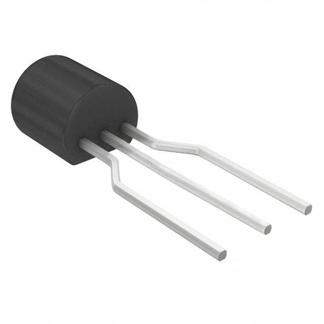
| 产品图片 |
|
| rohs | 符合RoHS无铅 / 符合限制有害物质指令(RoHS)规范要求 |
| 产品系列 | 晶体闸流管,SCR,ON Semiconductor 2N6028RLRAG- |
| 数据手册 | |
| 产品型号 | 2N6028RLRAG |
| 不重复通态电流 | 5 A |
| 产品目录页面 | |
| 产品种类 | SCR |
| 其它名称 | 2N6028RLRAGOSCT |
| 功率耗散(最大值) | 300mW |
| 商标 | ON Semiconductor |
| 安装风格 | Through Hole |
| 封装 | Reel |
| 封装/外壳 | TO-226-3、TO-92-3(TO-226AA)成形引线 |
| 封装/箱体 | TO-92 |
| 工厂包装数量 | 2000 |
| 最大工作温度 | + 100 C |
| 最大栅极峰值反向电压 | 5 V |
| 最小工作温度 | - 50 C |
| 标准包装 | 1 |
| 正向电压下降 | 1.5 V |
| 电压 | 40V |
| 电压-偏移(Vt) | 600mV |
| 电压-输出 | 11V |
| 电流-峰值 | 150nA |
| 电流-栅极至阳极漏(Igao) | 10nA |
| 电流-谷值(Iv) | 25µA |
| 系列 | 2N6028 |
| 额定重复关闭状态电压VDRM | 0.5 V |

,TO-226_straightlead.jpg)


- 商务部:美国ITC正式对集成电路等产品启动337调查
- 曝三星4nm工艺存在良率问题 高通将骁龙8 Gen1或转产台积电
- 太阳诱电将投资9.5亿元在常州建新厂生产MLCC 预计2023年完工
- 英特尔发布欧洲新工厂建设计划 深化IDM 2.0 战略
- 台积电先进制程称霸业界 有大客户加持明年业绩稳了
- 达到5530亿美元!SIA预计今年全球半导体销售额将创下新高
- 英特尔拟将自动驾驶子公司Mobileye上市 估值或超500亿美元
- 三星加码芯片和SET,合并消费电子和移动部门,撤换高东真等 CEO
- 三星电子宣布重大人事变动 还合并消费电子和移动部门
- 海关总署:前11个月进口集成电路产品价值2.52万亿元 增长14.8%
PDF Datasheet 数据手册内容提取
2N6027, 2N6028 Preferred Device Programmable Unijunction Transistor Programmable Unijunction Transistor Triggers http://onsemi.com Designed to enable the engineer to “program’’ unijunction characteristics such as RBB, (cid:2), IV, and IP by merely selecting PUTs two resistor values. Application includes thyristor−trigger, oscillator, 40 VOLTS, 300 mW pulse and timing circuits. These devices may also be used in special thyristor applications due to the availability of an anode gate. Supplied in an inexpensive TO−92 plastic package for high−volume G requirements, this package is readily adaptable for use in automatic A K insertion equipment. Features • Programmable − R , (cid:2), I and I BB V P • Low On−State Voltage − 1.5 V Maximum @ I = 50 mA F TO−92 (TO−226AA) • Low Gate to Anode Leakage Current − 10 nA Maximum CASE 029 • High Peak Output Voltage − 11 V Typical 1 STYLE 16 • Low Offset Voltage − 0.35 V Typical (R = 10 k(cid:3)) 23 G • Pb−Free Packages are Available* MARKING DIAGRAM 2N 602x AYWW(cid:2) (cid:2) 2N602x =Device Code x = 7 or 8 A =Assembly Location Y =Year WW =Work Week (cid:2) =Pb−Free Package (Note: Microdot may be in either location) PIN ASSIGNMENT 1 Anode 2 Gate 3 Cathode ORDERING INFORMATION See detailed ordering and shipping information in the package dimensions section on page 5 of this data sheet. *For additional information on our Pb−Free strategy and soldering details, please download the ON Semiconductor Soldering and Mounting Techniques Preferred devices are recommended choices for future use Reference Manual, SOLDERRM/D. and best overall value. © Semiconductor Components Industries, LLC, 2006 1 Publication Order Number: May, 2006 − Rev.6 2N6027/D
2N6027, 2N6028 MAXIMUM RATINGS (TJ = 25°C unless otherwise noted) Rating Symbol Value Unit Power Dissipation* PF 300 mW Derate Above 25°C 1/(cid:4)JA 4.0 mW/°C DC Forward Anode Current* IT 150 mA Derate Above 25°C 2.67 mA/°C DC Gate Current* IG (cid:2)50 mA Repetitive Peak Forward Current ITRM A 100 (cid:5)s Pulse Width, 1% Duty Cycle 1.0 20 (cid:5)s Pulse Width, 1% Duty Cycle* 2.0 Non−Repetitive Peak Forward Current ITSM 5.0 A 10 (cid:5)s Pulse Width Gate to Cathode Forward Voltage* VGKF 40 V Gate to Cathode Reverse Voltage* VGKR (cid:3)5.0 V Gate to Anode Reverse Voltage* VGAR 40 V Anode to Cathode Voltage* (Note 1) VAK ±40 V Capacitive Discharge Energy (Note 2) E 250 (cid:5)J Power Dissipation (Note 3) PD 300 mW Operating Temperature TOPR −50 to +100 °C Junction Temperature TJ −50 to +125 °C Storage Temperature Range Tstg −55 to +150 °C Stresses exceeding Maximum Ratings may damage the device. Maximum Ratings are stress ratings only. Functional operation above the Recommended Operating Conditions is not implied. Extended exposure to stresses above the Recommended Operating Conditions may affect device reliability. *Indicates JEDEC Registered Data 1. Anode positive, RGA = 1000 (cid:3) Anode negative, RGA = open 2. E = 0.5 (cid:2) CV2 capacitor discharge energy limiting resistor and repetition. 3. Derate current and power above 25°C. THERMAL CHARACTERISTICS Characteristic Symbol Max Unit Thermal Resistance, Junction−to−Case R(cid:4)JC 75 °C/W Thermal Resistance, Junction−to−Ambient R(cid:4)JA 200 °C/W Maximum Lead Temperature for Soldering Purposes TL 260 °C ((cid:4)1/16″ from case, 10 seconds maximum) http://onsemi.com 2
2N6027, 2N6028 ELECTRICAL CHARACTERISTICS (TC = 25°C unless otherwise noted) Characteristic Fig. No. Symbol Min Typ Max Unit Peak Current* 2,9,11 IP (cid:5)A (VS = 10 Vdc, RG = 1 M(cid:3)) 2N6027 − 1.25 2.0 2N6028 − 0.08 0.15 (VS = 10 Vdc, RG = 10 k(cid:3)) 2N6027 − 4.0 5.0 2N6028 − 0.70 1.0 Offset Voltage* 1 VT V (VS = 10 Vdc, RG = 1 M(cid:3)) 2N6027 0.2 0.70 1.6 2N6028 0.2 0.50 0.6 (VS = 10 Vdc, RG = 10 k(cid:3)) (Both Types) 0.2 0.35 0.6 Valley Current* 1,4,5 IV (cid:5)A (VS = 10 Vdc, RG = 1 M(cid:3)) 2N6027 − 18 50 2N6028 − 18 25 (VS = 10 Vdc, RG = 10 k (cid:3)) 2N6027 70 150 − 2N6028 25 150 − (VS = 10 Vdc, RG = 200 (cid:3)) 2N6027 1.5 − − 2N6028 1.0 − − mA Gate to Anode Leakage Current* − IGAO nAdc (VS = 40 Vdc, TA = 25°C, Cathode Open) − 1.0 10 (VS = 40 Vdc, TA = 75°C, Cathode Open) − 3.0 − Gate to Cathode Leakage Current − IGKS − 5.0 50 nAdc (VS = 40 Vdc, Anode to Cathode Shorted) Forward Voltage* 1,6 VF − 0.8 1.5 V (IF = 50 mA Peak) (Note 4) Peak Output Voltage* 3,7 Vo 6.0 11 − V (VG = 20 Vdc, CC = 0.2 (cid:5)F) Pulse Voltage Rise Time 3 tr − 40 80 ns (VB = 20 Vdc, CC = 0.2 (cid:5)F) *Indicates JEDEC Registered Data 4. Pulse Test: Pulse Width ≤ 300 (cid:5)s, Duty Cycle ≤ 2%. IA A +VB R2 IA RG = RR11 + R R22 VA VAK G R−1 VS = R1R +1 R2 VB VAK+ RG VS VS −VP VT = VP − VS K VF VV IA 1A − Programmable Unijunction 1B − Equivalent Test Circuit for IGAO IP IV IF Figure 1A used for electrical with (cid:2)Program" Resistors IC − Electrical Characteristics characteristics testing R1 and R2 (also see Figure 2) Figure 1. Electrical Characterization +VB − Adjust 100 k IP (SENSE) +V Turfno−ron 1.0% 100 +(cid:5)V = 1.0 nA 510 k 16 k Vo 6.0 V Threshold 2N5270 R VB RG = R/2 0.01 (cid:5)F VS = VB/2 CC vo 27 k Scope (See Figure 1) 20 (cid:3) 0.6 V t Put tf 20 Under R Test Figure 2. Peak Current (I ) Test Circuit Figure 3. V and t Test Circuit P o r http://onsemi.com 3
2N6027, 2N6028 TYPICAL VALLEY CURRENT BEHAVIOR 1000 500 A) A) (cid:5)ENT ( RG = 10 k(cid:3) (cid:5)ENT ( 100 RG = 10 k(cid:3) R R R R U U C 100 C EY 100 k(cid:3) EY L L L L VA VA 100 k(cid:3) I , V 1 M(cid:3) I , V 10 1 M(cid:3) 10 5 5 10 15 20 −50 −25 0 +25 +50 +75 +100 VS, SUPPLY VOLTAGE (V) TA, AMBIENT TEMPERATURE (°C) Figure 4. Effect of Supply Voltage Figure 5. Effect of Temperature 10 25 V) 5.0 TA = 25°C TA = 25°C CC = 0.2 (cid:5)F GE ( 2.0 E (V) 20 (SEE FIGURE 3) A G T A L 1.0 T O OL V V 15 D 0.5 T WAR 0.2 UTPU OR 0.1 K O 10 1000 pF F EA EAK 0.05 V , Po 5.0 P , P 0.02 V 0.01 0 0.01 0.02 0.05 0.1 0.2 0.5 1.0 2.0 5.0 0 5.0 10 15 20 25 30 35 40 IF, PEAK FORWARD CURRENT (AMP) VS, SUPPLY VOLTAGE (V) Figure 6. Forward Voltage Figure 7. Peak Output Voltage + B2 A A E R2 RT R2 G P G RBB = R1 + R2 A G N (cid:2) = R1 R1 + R2 P N R1 CC R1 K K K B1 Circuit Symbol Equivalent Circuit Typical Application with External (cid:2)Program" Resistors R1 and R2 Figure 8. Programmable Unijunction http://onsemi.com 4
2N6027, 2N6028 TYPICAL PEAK CURRENT BEHAVIOR 2N6027 10 100 50 5.0 (cid:5)T ( A) 3.0 (cid:5)T ( A) 20 (SEVES F =IG 1U0R VE 2) EN 2.0 EN 10 R R R R5.0 U U C 1.0 C AK RG = 10 k(cid:3) AK 2.0 E E I , PP00..53 100 k1(cid:3).0 M(cid:3) (SETEA F=I G2U5°RCE 2) I , PP10..05 RG = 10 1k(cid:3)00 k(cid:3) 0.2 1.0 M(cid:3) 0.2 0.1 0.1 5.0 10 15 20 −50 −25 0 +25 +50 +75 +100 VS, SUPPLY VOLTAGE (V) TA, AMBIENT TEMPERATURE (°C) Figure 9. Effect of Supply Voltage and R Figure 10. Effect of Temperature and R G G 2N6028 1.0 10 0.7 5.0 0.5 (cid:5)ENT ( A) 00..23 R1G0 0= k1(cid:3)0 k(cid:3) (cid:5)ENT ( A) 21..00 (SEVES F =IG 1U0R VE 2) R R R R 0.5 U U C 0.1 C AK 0.07 AK 0.2 RG = 10 k(cid:3) E E I , PP00..0053 1.0 M(cid:3) TA = 25°C I , PP00.0.15 100 k(cid:3) 0.02 (SEE FIGURE 2) 1.0 M(cid:3) 0.02 0.01 0.01 5.0 10 15 20 −50 −25 0 +25 +50 +75 +100 VS, SUPPLY VOLTAGE (V) TA, AMBIENT TEMPERATURE (°C) Figure 11. Effect of Supply Voltage and R Figure 12. Effect of Temperature and R G G ORDERING INFORMATION U.S. European Equivalent Shipping† Description of TO−92 Tape Orientation 2N6027 2N6027G 5000 Units / Box N/A − Bulk 2N6028 2N6028G 2N6027RLRA 2N6027RLRAG 2N6027RL1 2000 / Tape & Reel Round side of TO−92 and adhesive tape visible 2N6027RL1G 2N6028RLRA 2N6028RLRAG 2N6028RLRM Flat side of TO−92 and adhesive tape visible 2N6028RLRMG 2000 / Tape & Ammo Box 2N6028RLRP Round side of TO−92 and adhesive tape visible 2N6028RLRPG †For information on tape and reel specifications, including part orientation and tape sizes, please refer to our Tape and Reel Packaging Specifications Brochure, BRD8011/D. *The “G’’ suffix indicates Pb−Free package available. http://onsemi.com 5
2N6027, 2N6028 PACKAGE DIMENSIONS TO−92 (TO−226AA) CASE 029−11 ISSUE AL A NOTES: B 1. DIMENSIONING AND TOLERANCING PER ANSI Y14.5M, 1982. 2. CONTROLLING DIMENSION: INCH. R 3. CONTOUR OF PACKAGE BEYOND DIMENSION R IS UNCONTROLLED. 4. LEAD DIMENSION IS UNCONTROLLED IN P AND P BEYOND DIMENSION K MINIMUM. L SEATING INCHES MILLIMETERS PLANE K DIM MIN MAX MIN MAX A 0.175 0.205 4.45 5.20 B 0.170 0.210 4.32 5.33 C 0.125 0.165 3.18 4.19 X X D GD 00..001465 00..002515 0.14.0175 0.15.3339 G H 0.095 0.105 2.42 2.66 H J J 0.015 0.020 0.39 0.50 K 0.500 −−− 12.70 −−− V C L 0.250 −−− 6.35 −−− N 0.080 0.105 2.04 2.66 SECTION X−X P −−− 0.100 −−− 2.54 1 N R 0.115 −−− 2.93 −−− V 0.135 −−− 3.43 −−− N STYLE 16: PIN 1. ANODE 2. GATE 3. CATHODE ON Semiconductor and are registered trademarks of Semiconductor Components Industries, LLC (SCILLC). SCILLC reserves the right to make changes without further notice to any products herein. SCILLC makes no warranty, representation or guarantee regarding the suitability of its products for any particular purpose, nor does SCILLC assume any liability arising out of the application or use of any product or circuit, and specifically disclaims any and all liability, including without limitation special, consequential or incidental damages. “Typical” parameters which may be provided in SCILLC data sheets and/or specifications can and do vary in different applications and actual performance may vary over time. All operating parameters, including “Typicals” must be validated for each customer application by customer’s technical experts. SCILLC does not convey any license under its patent rights nor the rights of others. SCILLC products are not designed, intended, or authorized for use as components in systems intended for surgical implant into the body, or other applications intended to support or sustain life, or for any other application in which the failure of the SCILLC product could create a situation where personal injury or death may occur. Should Buyer purchase or use SCILLC products for any such unintended or unauthorized application, Buyer shall indemnify and hold SCILLC and its officers, employees, subsidiaries, affiliates, and distributors harmless against all claims, costs, damages, and expenses, and reasonable attorney fees arising out of, directly or indirectly, any claim of personal injury or death associated with such unintended or unauthorized use, even if such claim alleges that SCILLC was negligent regarding the design or manufacture of the part. SCILLC is an Equal Opportunity/Affirmative Action Employer. This literature is subject to all applicable copyright laws and is not for resale in any manner. PUBLICATION ORDERING INFORMATION LITERATURE FULFILLMENT: N. American Technical Support: 800−282−9855 Toll Free ON Semiconductor Website: www.onsemi.com Literature Distribution Center for ON Semiconductor USA/Canada P.O. Box 5163, Denver, Colorado 80217 USA Europe, Middle East and Africa Technical Support: Order Literature: http://www.onsemi.com/orderlit Phone: 303−675−2175 or 800−344−3860 Toll Free USA/Canada Phone: 421 33 790 2910 Fax: 303−675−2176 or 800−344−3867 Toll Free USA/Canada Japan Customer Focus Center For additional information, please contact your local Email: orderlit@onsemi.com Phone: 81−3−5773−3850 Sales Representative http://onsemi.com 2N6027/D 6