ICGOO在线商城 > 分立半导体产品 > 晶体管 - 可编程单结 > 2N6027RL1G
 Datasheet下载
- 型号: 2N6027RL1G
- 制造商: ON Semiconductor
- 库位|库存: xxxx|xxxx
- 要求:
| 数量阶梯 | 香港交货 | 国内含税 |
| +xxxx | $xxxx | ¥xxxx |
查看当月历史价格
查看今年历史价格
2N6027RL1G产品简介:
ICGOO电子元器件商城为您提供2N6027RL1G由ON Semiconductor设计生产,在icgoo商城现货销售,并且可以通过原厂、代理商等渠道进行代购。 2N6027RL1G价格参考。ON Semiconductor2N6027RL1G封装/规格:晶体管 - 可编程单结, Programmable Unijunction Transistor (UJT) 40V 300mW TO-226-3, TO-92-3 (TO-226AA) (Formed Leads)。您可以下载2N6027RL1G参考资料、Datasheet数据手册功能说明书,资料中有2N6027RL1G 详细功能的应用电路图电压和使用方法及教程。
2N6027RL1G 是一款由 ON Semiconductor(安森美半导体)生产的可编程单结晶体管(Programmable Unijunction Transistor,PUT)。这种器件广泛应用于需要精确触发和控制的电路中,尤其适合以下应用场景:

 1. 脉冲发生器
   - 2N6027RL1G 可用于设计定时电路或脉冲发生器。通过调整外部电阻和电容值,可以生成特定频率和宽度的脉冲信号,适用于时钟信号生成、触发信号控制等场景。

 2. 触发电路
   - 在 SCR(可控硅整流器)或 TRIAC(双向晶闸管)驱动电路中,2N6027RL1G 能够作为触发电路的核心元件。它可以根据输入电压的变化,精确地触发后续功率器件,用于调光、电机控制或电源管理。

 3. 振荡器
   - 利用其负阻特性和可编程特性,2N6027RL1G 可构建弛张振荡器(Relaxation Oscillator)。这类振荡器常用于信号源、电子音乐合成器或通信设备中的载波生成。

 4. 过压保护
   - 该晶体管可用作过压检测和保护电路的一部分。当输入电压超过预设阈值时,2N6027RL1G 会导通并触发保护机制,防止后端电路受损。

 5. 开关应用
   - 在低功耗开关应用中,2N6027RL1G 提供了稳定的触发性能和高可靠性,适用于电池供电设备或其他对能耗敏感的系统。

 6. 电子实验与教育
   - 由于其简单易用且功能多样,2N6027RL1G 常被用作教学工具,帮助学生理解 PUT 的工作原理及其在实际电路中的应用。

总之,2N6027RL1G 的灵活性使其成为许多模拟和混合信号电路设计的理想选择,特别适合需要精确触发和定时控制的应用场合。
| 参数 | 数值 |
| 产品目录 | |
| 描述 | THYRISTOR PROG UNIJUNCT 40V TO92SCR 40V 300mW PUT |
| 产品分类 | 可编程单结晶体管(PUT)分离式半导体 |
| 品牌 | ON Semiconductor |
| 产品手册 | |
| 产品图片 |
|
| rohs | 符合RoHS无铅 / 符合限制有害物质指令(RoHS)规范要求 |
| 产品系列 | 晶体闸流管,SCR,ON Semiconductor 2N6027RL1G- |
| 数据手册 | |
| 产品型号 | 2N6027RL1G |
| 不重复通态电流 | 5 A |
| 产品种类 | SCR |
| 其它名称 | 2N6027RL1GOSCT |
| 功率耗散(最大值) | 300mW |
| 商标 | ON Semiconductor |
| 安装风格 | Through Hole |
| 封装 | Reel |
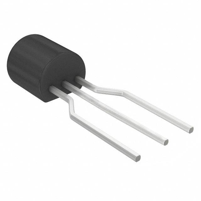
| 封装/外壳 | TO-226-3、TO-92-3(TO-226AA)成形引线 |
| 封装/箱体 | TO-92-3 (TO-226) |
| 工厂包装数量 | 2000 |
| 最大工作温度 | + 100 C |
| 最大栅极峰值反向电压 | 5 V |
| 最小工作温度 | - 50 C |
| 标准包装 | 1 |
| 电压 | 40V |
| 电压-偏移(Vt) | 1.6V |
| 电压-输出 | 11V |
| 电流-峰值 | 2µA |
| 电流-栅极至阳极漏(Igao) | 10nA |
| 电流-谷值(Iv) | 50µA |
| 系列 | 2N6027 |
| 额定重复关闭状态电压VDRM | 40 V |

,TO-226_straightlead.jpg)


- 商务部:美国ITC正式对集成电路等产品启动337调查
- 曝三星4nm工艺存在良率问题 高通将骁龙8 Gen1或转产台积电
- 太阳诱电将投资9.5亿元在常州建新厂生产MLCC 预计2023年完工
- 英特尔发布欧洲新工厂建设计划 深化IDM 2.0 战略
- 台积电先进制程称霸业界 有大客户加持明年业绩稳了
- 达到5530亿美元!SIA预计今年全球半导体销售额将创下新高
- 英特尔拟将自动驾驶子公司Mobileye上市 估值或超500亿美元
- 三星加码芯片和SET,合并消费电子和移动部门,撤换高东真等 CEO
- 三星电子宣布重大人事变动 还合并消费电子和移动部门
- 海关总署:前11个月进口集成电路产品价值2.52万亿元 增长14.8%

PDF Datasheet 数据手册内容提取
(cid:4)(cid:8)(cid:5)(cid:3)(cid:4)(cid:6)(cid:2) (cid:4)(cid:8)(cid:5)(cid:3)(cid:4)(cid:7) Preferred Device (cid:9)(cid:23)(cid:22)(cid:16)(cid:23)(cid:12)(cid:20)(cid:20)(cid:12)(cid:13)(cid:19)(cid:15) (cid:11)(cid:21)(cid:17)(cid:18)(cid:26)(cid:21)(cid:14)(cid:25)(cid:17)(cid:22)(cid:21) (cid:10)(cid:23)(cid:12)(cid:21)(cid:24)(cid:17)(cid:24)(cid:25)(cid:22)(cid:23) Programmable Unijunction Transistor Triggers Designed to enable the engineer to “program’’ unijunction http://onsemi.com characteristics such as RBB, h , IV, and IP by merely selecting two resistor values. Application includes thyristor–trigger, oscillator, pulse PUTs and timing circuits. These devices may also be used in special thyristor 40 VOLTS applications due to the availability of an anode gate. Supplied in an 300 mW inexpensive TO–92 plastic package for high–volume requirements, this package is readily adaptable for use in automatic insertion equipment. • Programmable — RBB, h , IV and IP G • Low On–State Voltage — 1.5 Volts Maximum @ IF = 50 mA A K • Low Gate to Anode Leakage Current — 10 nA Maximum • High Peak Output Voltage — 11 Volts Typical • Low Offset Voltage — 0.35 Volt Typical (RG = 10 k ohms) • Device Marking: Logo, Device Type, e.g., 2N6027, Date Code MAXIMUM RATINGS (TJ = 25°C unless otherwise noted) Rating Symbol Value Unit 1 *Power Dissipation PF 300 mW 23 Derate Above 25°C 1/q JA 4.0 mW/°C *DC Forward Anode Current IT 150 mA TO–92 (TO–226AA) Derate Above 25°C 2.67 mA/°C CASE 029 STYLE 16 *DC Gate Current IG (cid:1)50 mA Repetitive Peak Forward Current ITRM Amps PIN ASSIGNMENT 100 m s Pulse Width, 1% Duty Cycle 1.0 *20 m s Pulse Width, 1% Duty Cycle 2.0 1 Anode 2 Gate Non–Repetitive Peak Forward Current ITSM 5.0 Amps 10 m s Pulse Width 3 Cathode *Gate to Cathode Forward Voltage VGKF 40 Volts *Gate to Cathode Reverse Voltage VGKR (cid:2)5.0 Volts ORDERING INFORMATION *Gate to Anode Reverse Voltage VGAR 40 Volts See detailed ordering and shipping information in the package *Anode to Cathode Voltage(1) VAK (cid:1)40 Volts dimensions section on page 7 of this data sheet. Operating Junction Temperature Range TJ –50 to °C Preferred devices are recommended choices for future use +100 and best overall value. *Storage Temperature Range Tstg –55 to °C +150 *Indicates JEDEC Registered Data (1)Anode positive, RGA = 1000 ohms Anode negative, RGA = open Semiconductor Components Industries, LLC, 2000 1 Publication Order Number: May, 2000 – Rev. 2 2N6027/D
2N6027, 2N6028 THERMAL CHARACTERISTICS Characteristic Symbol Max Unit Thermal Resistance, Junction to Case Rq JC 75 °C/W Thermal Resistance, Junction to Ambient Rq JA 200 °C/W Maximum Lead Temperature for Soldering Purposes TL 260 °C ((cid:1)1/16″ from case, 10 secs max) ELECTRICAL CHARACTERISTICS (TC = 25°C unless otherwise noted.) Characteristic Fig. No. Symbol Min Typ Max Unit *Peak Current 2,9,11 IP m A (VS = 10 Vdc, RG = 1 MW) 2N6027 — 1.25 2.0 2N6028 — 0.08 0.15 (VS = 10 Vdc, RG = 10 k ohms) 2N6027 — 4.0 5.0 2N6028 — 0.70 1.0 *Offset Voltage 1 VT Volts (VS = 10 Vdc, RG = 1 MW) 2N6027 0.2 0.70 1.6 2N6028 0.2 0.50 0.6 (VS = 10 Vdc, RG = 10 k ohms) (Both Types) 0.2 0.35 0.6 *Valley Current 1,4,5 IV m A (VS = 10 Vdc, RG = 1 MW) 2N6027 — 18 50 2N6028 — 18 25 (VS = 10 Vdc, RG = 10 k ohms) 2N6027 70 150 — 2N6028 25 150 — (VS = 10 Vdc, RG = 200 ohms) 2N6027 1.5 — — mA 2N6028 1.0 — — *Gate to Anode Leakage Current — IGAO nAdc (VS = 40 Vdc, TA = 25°C, Cathode Open) — 1.0 10 (VS = 40 Vdc, TA = 75°C, Cathode Open) — 3.0 — Gate to Cathode Leakage Current — IGKS — 5.0 50 nAdc (VS = 40 Vdc, Anode to Cathode Shorted) *Forward Voltage (IF = 50 mA Peak)(1) 1,6 VF — 0.8 1.5 Volts *Peak Output Voltage 3,7 Vo 6.0 11 — Volt (VG = 20 Vdc, CC = 0.2 m F) Pulse Voltage Rise Time 3 tr — 40 80 ns (VB = 20 Vdc, CC = 0.2 m F) *Indicates JEDEC Registered Data (1)Pulse Test: Pulse Width ≤ 300 m sec, Duty Cycle ≤ 2%. http://onsemi.com 2
2N6027, 2N6028 +VB IA R1 R2 VA IA A R2 RG = R1 + R2 G – VS = R1 VB + VS –VP R1 + R2 RG VT = VP – VS VAK R1 VAK VS K VF VV IA 1A – Programmable Unijunction 1B – Equivalent Test Circuit for IGAO IP IV IF Figure 1A used for electrical with “Program” Resistors IC – Electrical Characteristics characteristics testing R1 and R2 (also see Figure 2) Figure 1. Electrical Characterization +VB – Adjust 100k IP (SENSE) +V Turfno–ron 1.0% 100 +m V = 1.0 nA 510k 16k Vo 6 V Threshold 2N5270 R VB RG = R/2 0.01 m F VS = VB/2 CC vo 27k Scope (See Figure 1) 20 W 0.6 V t Put tf 20 Under R Test Figure 2. Peak Current (IP) Test Circuit Figure 3. Vo and tr Test Circuit http://onsemi.com 3
2N6027, 2N6028 TYPICAL VALLEY CURRENT BEHAVIOR 1000 500 A) A) mENT ( RG = 10 kW mENT ( 100 RG = 10 kW R R R R U U C 100 C EY 100 kW EY L L L L VA VA 100 kW I , V 1 MW I , V 10 1 MW 10 5 5 10 15 20 –50 –25 0 +25 +50 +75 +100 VS, SUPPLY VOLTAGE (VOLTS) TA, AMBIENT TEMPERATURE (°C) Figure 4. Effect of Supply Voltage Figure 5. Effect of Temperature 10 25 S) 5.0 TA = 25°C TA = 25°C CC = 0.2 m F LT S) (SEE FIGURE 3) LTAGE (VO 12..00 AGE (VOLT 2105 D VO 0.5 VOLT WAR 0.2 PUT 10 OR 0.1 UT 1000 pF F O K 0.05 K EA EA 5.0 P P V , F0.02 V , o 0.01 0 0.01 0.02 0.05 0.1 0.2 0.5 1.0 2.0 5.0 0 5.0 10 15 20 25 30 35 40 IF, PEAK FORWARD CURRENT (AMP) VS, SUPPLY VOLTAGE (VOLTS) Figure 6. Forward Voltage Figure 7. Peak Output Voltage + B2 A A E R2 RT R2 G P G RBB = R1 + R2 A G N h = R1 R1 + R2 P N R1 CC R1 K K K B1 Circuit Symbol Equivalent Circuit Typical Application with External “Program” Resistors R1 and R2 Figure 8. Programmable Unijunction http://onsemi.com 4
2N6027, 2N6028 TYPICAL PEAK CURRENT BEHAVIOR 2N6027 10 100 50 5.0 mENT ( A) 23..00 mENT ( A) 2100 (VSSE E= F1I0G VUORLET S2) R R R R5.0 U U C 1.0 C AK RG = 10 kW AK 2.0 E E I , PP 0.5 100 kW TA = 25°C I , PP1.0 RG = 10 kW 0.3 1.0 MW (SEE FIGURE 2) 0.5 100 kW 0.2 1.0 MW 0.2 0.1 0.1 5.0 10 15 20 –50 –25 0 +25 +50 +75 +100 VS, SUPPLY VOLTAGE (VOLTS) TA, AMBIENT TEMPERATURE (°C) Figure 9. Effect of Supply Voltage and RG Figure 10. Effect of Temperature and RG 2N6028 1.0 10 0.7 5.0 0.5 mENT ( A) 00..23 R1G0 0= k1W0 kW mENT ( A) 21..00 (VSSE E= F1I0G VUORLET S2) R R R R 0.5 U U C 0.1 C AK 0.07 AK 0.2 RG = 10 kW E E I , PP 00..0053 1.0 MW TA = 25°C I , PP00.0.15 100 kW 0.02 (SEE FIGURE 2) 1.0 MW 0.02 0.01 0.01 5.0 10 15 20 –50 –25 0 +25 +50 +75 +100 VS, SUPPLY VOLTAGE (VOLTS) TA, AMBIENT TEMPERATURE (°C) Figure 11. Effect of Supply Voltage and RG Figure 12. Effect of Temperature and RG http://onsemi.com 5
2N6027, 2N6028 TO–92 EIA RADIAL TAPE IN FAN FOLD BOX OR ON REEL H2A H2A H2B H2B H W2 H4H5 T1 L1 H1 W1 W L T F1 T2 F2 P2 P2 D P1 P Figure 13. Device Positioning on Tape Specification Inches Millimeter Symbol Item Min Max Min Max D Tape Feedhole Diameter 0.1496 0.1653 3.8 4.2 D2 Component Lead Thickness Dimension 0.015 0.020 0.38 0.51 F1, F2 Component Lead Pitch 0.0945 0.110 2.4 2.8 H Bottom of Component to Seating Plane .059 .156 1.5 4.0 H1 Feedhole Location 0.3346 0.3741 8.5 9.5 H2A Deflection Left or Right 0 0.039 0 1.0 H2B Deflection Front or Rear 0 0.051 0 1.0 H4 Feedhole to Bottom of Component 0.7086 0.768 18 19.5 H5 Feedhole to Seating Plane 0.610 0.649 15.5 16.5 L Defective Unit Clipped Dimension 0.3346 0.433 8.5 11 L1 Lead Wire Enclosure 0.09842 — 2.5 — P Feedhole Pitch 0.4921 0.5079 12.5 12.9 P1 Feedhole Center to Center Lead 0.2342 0.2658 5.95 6.75 P2 First Lead Spacing Dimension 0.1397 0.1556 3.55 3.95 T Adhesive Tape Thickness 0.06 0.08 0.15 0.20 T1 Overall Taped Package Thickness — 0.0567 — 1.44 T2 Carrier Strip Thickness 0.014 0.027 0.35 0.65 W Carrier Strip Width 0.6889 0.7481 17.5 19 W1 Adhesive Tape Width 0.2165 0.2841 5.5 6.3 W2 Adhesive Tape Position .0059 0.01968 .15 0.5 NOTES: 1. Maximum alignment deviation between leads not to be greater than 0.2 mm. 2. Defective components shall be clipped from the carrier tape such that the remaining protrusion (L) does not exceed a maximum of 11 mm. 3. Component lead to tape adhesion must meet the pull test requirements. 4. Maximum non–cumulative variation between tape feed holes shall not exceed 1 mm in 20 pitches. 5. Holddown tape not to extend beyond the edge(s) of carrier tape and there shall be no exposure of adhesive. 6. No more than 1 consecutive missing component is permitted. 7. A tape trailer and leader, having at least three feed holes is required before the first and after the last component. 8. Splices will not interfere with the sprocket feed holes. http://onsemi.com 6
2N6027, 2N6028 ORDERING & SHIPPING INFORMATION: 2N6027 and 2N6028 packaging options, Device Suffix Europe U.S. Equivalent Shipping Description of TO92 Tape Orientation 2N6027, 2N6028 Bulk in Box (5K/Box) N/A, Bulk 2N6027, 2N6028RLRA Radial Tape and Reel (2K/Reel) Round side of TO92 and adhesive tape visible 2N6027RL1 Radial Tape and Reel (2K/Reel) Flat side of TO92 and adhesive tape visible 2N6028RLRM Radial Tape and Fan Fold Box (2K/Box) Flat side of TO92 and adhesive tape visible 2N6028RLRP Radial Tape and Fan Fold Box (2K/Box) Round side of TO92 and adhesive tape visible PACKAGE DIMENSIONS TO–92 (TO–226AA) CASE 029–11 ISSUE AJ NOTES: A B 1. DIMENSIONING AND TOLERANCING PER ANSI Y14.5M, 1982. 2. CONTROLLING DIMENSION: INCH. 3. CONTOUR OF PACKAGE BEYOND DIMENSION R R IS UNCONTROLLED. 4. LEAD DIMENSION IS UNCONTROLLED IN P AND P BEYOND DIMENSION K MINIMUM. L SEATING INCHES MILLIMETERS PLANE K DIM MIN MAX MIN MAX A 0.175 0.205 4.45 5.20 B 0.170 0.210 4.32 5.33 C 0.125 0.165 3.18 4.19 D 0.016 0.021 0.407 0.533 X X D G 0.045 0.055 1.15 1.39 G H 0.095 0.105 2.42 2.66 H J J 0.015 0.020 0.39 0.50 K 0.500 ––– 12.70 ––– V C L 0.250 ––– 6.35 ––– N 0.080 0.105 2.04 2.66 SECTION X–X P ––– 0.100 ––– 2.54 1 N R 0.115 ––– 2.93 ––– V 0.135 ––– 3.43 ––– N STYLE 16: PIN 1. ANODE 2. GATE 3. CATHODE http://onsemi.com 7
2N6027, 2N6028 ON Semiconductor and are trademarks of Semiconductor Components Industries, LLC (SCILLC). SCILLC reserves the right to make changes without further notice to any products herein. SCILLC makes no warranty, representation or guarantee regarding the suitability of its products for any particular purpose, nor does SCILLC assume any liability arising out of the application or use of any product or circuit, and specifically disclaims any and all liability, including without limitation special, consequential or incidental damages. “Typical” parameters which may be provided in SCILLC data sheets and/or specifications can and do vary in different applications and actual performance may vary over time. All operating parameters, including “Typicals” must be validated for each customer application by customer’s technical experts. SCILLC does not convey any license under its patent rights nor the rights of others. SCILLC products are not designed, intended, or authorized for use as components in systems intended for surgical implant into the body, or other applications intended to support or sustain life, or for any other application in which the failure of the SCILLC product could create a situation where personal injury or death may occur. Should Buyer purchase or use SCILLC products for any such unintended or unauthorized application, Buyer shall indemnify and hold SCILLC and its officers, employees, subsidiaries, affiliates, and distributors harmless against all claims, costs, damages, and expenses, and reasonable attorney fees arising out of, directly or indirectly, any claim of personal injury or death associated with such unintended or unauthorized use, even if such claim alleges that SCILLC was negligent regarding the design or manufacture of the part. SCILLC is an Equal Opportunity/Affirmative Action Employer. PUBLICATION ORDERING INFORMATION NORTH AMERICA Literature Fulfillment: CENTRAL/SOUTH AMERICA: Literature Distribution Center for ON Semiconductor Spanish Phone: 303–308–7143 (Mon–Fri 8:00am to 5:00pm MST) P.O. Box 5163, Denver, Colorado 80217 USA Email: ONlit–spanish@hibbertco.com Phone: 303–675–2175 or 800–344–3860 Toll Free USA/Canada Fax: 303–675–2176 or 800–344–3867 Toll Free USA/Canada ASIA/PACIFIC: LDC for ON Semiconductor – Asia Support Email: ONlit@hibbertco.com Phone: 303–675–2121 (Tue–Fri 9:00am to 1:00pm, Hong Kong Time) Fax Response Line: 303–675–2167 or 800–344–3810 Toll Free USA/Canada Toll Free from Hong Kong & Singapore: 001–800–4422–3781 N. American Technical Support: 800–282–9855 Toll Free USA/Canada Email: ONlit–asia@hibbertco.com EUROPE: LDC for ON Semiconductor – European Support JAPAN: ON Semiconductor, Japan Customer Focus Center GermanPhone: (+1) 303–308–7140 (M–F 1:00pm to 5:00pm Munich Time) 4–32–1 Nishi–Gotanda, Shinagawa–ku, Tokyo, Japan 141–8549 Email: ONlit–german@hibbertco.com Phone: 81–3–5740–2745 French Phone: (+1) 303–308–7141 (M–F 1:00pm to 5:00pm Toulouse Time) Email: r14525@onsemi.com Email: ONlit–french@hibbertco.com English Phone: (+1) 303–308–7142 (M–F 12:00pm to 5:00pm UK Time) ON Semiconductor Website: http://onsemi.com Email: ONlit@hibbertco.com EUROPEAN TOLL–FREE ACCESS*: 00–800–4422–3781 For additional information, please contact your local *Available from Germany, France, Italy, England, Ireland Sales Representative. http://onsemi.com 2N6027/D 8