
 Datasheet下载
- 型号: 24LC01BT-I/OT
- 制造商: Microchip
- 库位|库存: xxxx|xxxx
- 要求:
| 数量阶梯 | 香港交货 | 国内含税 |
| +xxxx | $xxxx | ¥xxxx |
查看当月历史价格
查看今年历史价格
24LC01BT-I/OT产品简介:
ICGOO电子元器件商城为您提供24LC01BT-I/OT由Microchip设计生产,在icgoo商城现货销售,并且可以通过原厂、代理商等渠道进行代购。 24LC01BT-I/OT价格参考。Microchip24LC01BT-I/OT封装/规格:存储器, EEPROM 存储器 IC 1Kb (128 x 8) I²C 400kHz 3500ns SOT-23-5。您可以下载24LC01BT-I/OT参考资料、Datasheet数据手册功能说明书,资料中有24LC01BT-I/OT 详细功能的应用电路图电压和使用方法及教程。
24LC01BT-I/OT 是由 Microchip Technology 生产的一款 EEPROM(电可擦可编程只读存储器),属于存储器类器件。该型号的应用场景主要包括以下方面:

1. 数据存储:24LC01BT-I/OT 提供 1 Kbit 的存储容量,适用于需要小容量非易失性存储的应用,如保存设备配置参数、校准数据或用户设置等。

2. 工业控制:在工业自动化领域,这款 EEPROM 可用于存储控制器的运行参数、故障记录或诊断信息,确保断电后数据不丢失。

3. 消费电子:在家电或其他消费类电子产品中,可用于保存时间设置、语言偏好或个性化配置信息,例如时钟、遥控器或打印机设置。

4. 通信设备:适用于存储网络设备的 MAC 地址、序列号或其他唯一标识信息,确保设备身份的持久性和唯一性。

5. 医疗设备:可用于存储患者的测量数据、校准值或设备使用记录,满足医疗行业对数据可靠性和准确性的要求。

6. 汽车电子:在汽车系统中,可以用于存储座椅位置、后视镜角度或驾驶习惯等个性化设置,提升用户体验。

7. 物联网(IoT):在低功耗 IoT 设备中,可用于存储传感器校准数据、网络配置或设备状态信息,支持设备的长期稳定运行。

这款芯片采用 I²C 接口,支持高达 400 kHz 的通信速度,适合对功耗和体积有严格要求的嵌入式应用。其工作电压范围为 2.5V 至 5.5V,适应多种供电环境,同时具备高可靠性,能够在 -40°C 至 +85°C 的温度范围内正常工作。这些特性使其成为许多低功耗、小型化应用的理想选择。
| 参数 | 数值 |
| 产品目录 | 集成电路 (IC)半导体 |
| 描述 | IC EEPROM 1KBIT 400KHZ SOT23-5电可擦除可编程只读存储器 128x8 - 1.8V |
| 产品分类 | |
| 品牌 | Microchip Technology |
| 产品手册 | |
| 产品图片 |
|
| rohs | 符合RoHS无铅 / 符合限制有害物质指令(RoHS)规范要求 |
| 产品系列 | 内存,电可擦除可编程只读存储器,Microchip Technology 24LC01BT-I/OT- |
| 数据手册 | http://www.microchip.com/mymicrochip/filehandler.aspx?ddocname=en011831 |
| 产品型号 | 24LC01BT-I/OT |
| 产品培训模块 | http://www.digikey.cn/PTM/IndividualPTM.page?site=cn&lang=zhs&ptm=4315 |
| 产品目录页面 | |
| 产品种类 | 电可擦除可编程只读存储器 |
| 供应商器件封装 | SOT-23-5 |
| 其它名称 | 24LC01BT-I/OTCT |
| 包装 | 剪切带 (CT) |
| 商标 | Microchip Technology |
| 存储器类型 | EEPROM |
| 存储容量 | 1K (128 x 8) |
| 安装风格 | SMD/SMT |
| 封装 | Reel |
| 封装/外壳 | SC-74A,SOT-753 |
| 封装/箱体 | SOT-23-5 |
| 工作温度 | -40°C ~ 85°C |
| 工作电流 | 3 mA |
| 工作电源电压 | 2.5 V, 5.5 V |
| 工厂包装数量 | 3000 |
| 接口 | I²C,2 线串口 |
| 接口类型 | I2C |
| 数据保留 | 200 yr |
| 最大工作温度 | + 85 C |
| 最大工作电流 | 3 mA |
| 最大时钟频率 | 0.4 MHz |
| 最小工作温度 | - 40 C |
| 标准包装 | 1 |
| 格式-存储器 | EEPROMs - 串行 |
| 电压-电源 | 2.5 V ~ 5.5 V |
| 电源电压-最大 | 5.5 V |
| 电源电压-最小 | 2.5 V |
| 组织 | 128 x 8 |
| 访问时间 | 900 ns |
| 速度 | 400kHz |


- 商务部:美国ITC正式对集成电路等产品启动337调查
- 曝三星4nm工艺存在良率问题 高通将骁龙8 Gen1或转产台积电
- 太阳诱电将投资9.5亿元在常州建新厂生产MLCC 预计2023年完工
- 英特尔发布欧洲新工厂建设计划 深化IDM 2.0 战略
- 台积电先进制程称霸业界 有大客户加持明年业绩稳了
- 达到5530亿美元!SIA预计今年全球半导体销售额将创下新高
- 英特尔拟将自动驾驶子公司Mobileye上市 估值或超500亿美元
- 三星加码芯片和SET,合并消费电子和移动部门,撤换高东真等 CEO
- 三星电子宣布重大人事变动 还合并消费电子和移动部门
- 海关总署:前11个月进口集成电路产品价值2.52万亿元 增长14.8%
_renders/IS42S32800D-6BLI.jpg)


PDF Datasheet 数据手册内容提取
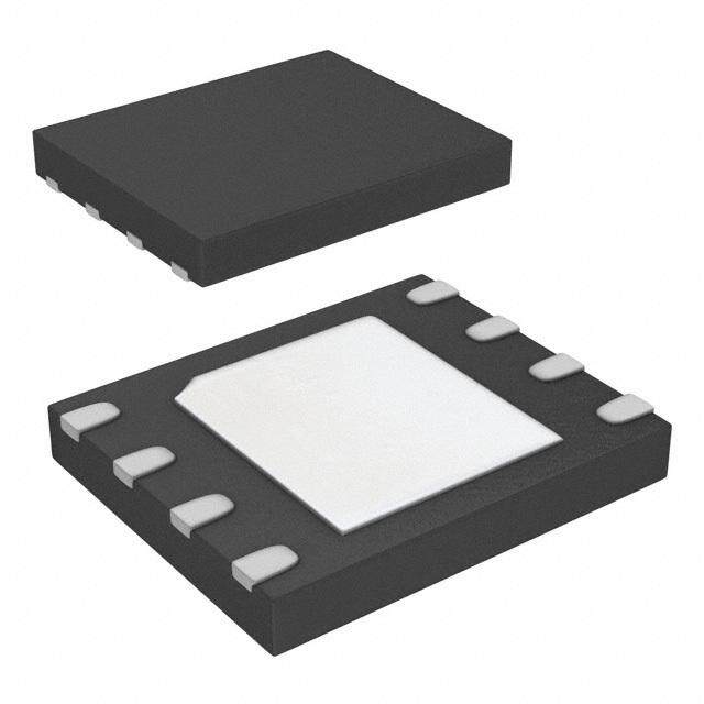
24AA01/24LC01B/24FC01 2 1K I C Serial EEPROM Device Selection Table Part Number VCC Range Max. Clock Frequency Temp. Ranges Available Packages 24AA01 1.7V-5.5V 400kHz(1) I P, SN, MS, ST, MC, LT, MNY, OT 24LC01B 2.5V-5.5V 400kHz I, E P, SN, MS, ST, MC, LT, MNY, OT 24FC01 1.7V-5.5V 1MHz I, E P, SN, MS, ST, MUY, OT Note1: 100kHz for VCC<2.5V Features Description • Single Supply with Operation down to 1.7V for The Microchip Technology Inc. 24XX01(1) is a 1Kbit 24AAXX and 24FCXX Devices, 2.5V for 24LCXX Electrically Erasable PROM. The device is organized Devices as one block of 128x8-bit memory with a 2-wire serial • Low-Power CMOS Technology: interface. Its low-voltage design permits operation down to 1.7V with standby and active currents of only - Read current 1mA, maximum 1µA and 1mA, respectively. The 24XX01 also has a - Standby current 1µA, maximum (I-temp.) page write capability for up to 8bytes of data. • 2-Wire Serial Interface, I2C Compatible • Schmitt Trigger Inputs for Noise Suppression • Output Slope Control to Eliminate Ground Bounce Note1: 24XX01 is used in this document as a generic part number for the • 100kHz, 400kHz and 1MHz Compatibility 24AA01/24LC01B/24FC01 devices. • Page Write Time: 5ms, Maximum • Self-Timed Erase/Write Cycle Package Types • 8-Byte Page Write Buffer • Hardware Write-Protect PDIP, MSOP DFN/TDFN/UDFN (Top View) • ESD Protection >4,000V (Top View) • More than 1 Million Erase/Write Cycles A0( 1 ) 1 8 VCC A0( 1 ) 1 8 VCC • Data Retention >200 Years A1( 1 ) 2 7 WP A1( 1 ) 2 7 WP • Factory Programming Available A2( 1 ) 3 6 SCL A2( 1 ) 3 6 SCL • RoHS Compliant VSS 4 5 SDA VSS 4 5 SDA • Temperature Ranges: - Industrial (I): -40°C to +85°C SOIC, TSSOP - Extended (E): -40°C to +125°C (Top View) SOT-23/SC-70 • Automotive AEC-Q100 Qualified (Top View) A0( 1 ) 1 8 VCC Packages: A1( 1 ) 2 7 WP SCL 1 5 WP A2( 1 ) 3 6 SCL Vss 2 • 8-Lead DFN, 8-Lead MSOP, 8-Lead PDIP, 8-Lead SOIC, 8-Lead TDFN, 8-Lead TSSOP, 8-Lead VSS 4 5 SDA SDA 3 4 Vcc UDFN, 5-Lead SOT-23 and 5-Lead SC-70 Note 1: Pins A0, A1 and A2 are not used by the 24XX01 (no internal connections). 2009-2018 Microchip Technology Inc. DS20001711K-page 1
24AA01/24LC01B/24FC01 Block Diagram WP HV Generator I/O Memory EEPROM Control Control XDEC Array Logic Logic Page Latches I/O SCL YDEC SDA VCC VSS Sense Amp. R/W Control DS20001711K-page 2 2009-2018 Microchip Technology Inc.
24AA01/24LC01B/24FC01 1.0 ELECTRICAL CHARACTERISTICS Absolute Maximum Ratings (†) VCC.............................................................................................................................................................................6.5V All inputs and outputs w.r.t. VSS..........................................................................................................-0.3V to VCC +1.0V Storage temperature...............................................................................................................................-65°C to +150°C Ambient temperature with power applied................................................................................................-40°C to +125°C ESD protection on all pins4kV † NOTICE: Stresses above those listed under “Absolute Maximum Ratings” may cause permanent damage to the device. This is a stress rating only and functional operation of the device at those or any other conditions above those indicated in the operational listings of this specification is not implied. Exposure to maximum rating conditions for extended periods may affect device reliability. TABLE 1-1: DC CHARACTERISTICS Industrial (I): TA = -40°C to +85°C, VCC = +1.7V to +5.5V DC CHARACTERISTICS Extended (E): TA = -40°C to +125°C, VCC = +2.5V to +5.5V (24LC01B) Extended (E): TA = -40°C to +125°C, VCC = +1.7V to +5.5V (24FC01) Param. Symbol Characteristic Min. Typ. Max. Units Conditions No. D1 VIH High-Level Input Voltage 0.7 VCC — — V D2 VIL Low-Level Input Voltage — — 0.3 VCC V D3 VHYS Hysteresis of Schmitt 0.05 VCC — — V (Note) Trigger Inputs D4 VOL Low-Level Output — — 0.40 V IOL=3.0mA, VCC=2.5V Voltage D5 ILI Input Leakage Current — — ±1 µA VIN=VSS or VCC D6 ILO Output Leakage Current — — ±1 µA VOUT=VSS or VCC D7 CIN, Pin Capacitance — — 10 pF VCC = 5.0V (Note) COUT (all inputs/outputs) TA = 25°C, FCLK=1MHz D8 ICCWRITE Operating Current — — 3 mA VCC = 5.5V, SCL = 400kHz D9 ICCREAD — — 1 mA VCC = 5.5V, SCL = 400kHz D10 ICCS Standby Current — — 1 µA SDA = SCL = VCC WP = V , I-Temp. SS — — 3 µA SDA = SCL = VDD WP = V , E-Temp. (24FC01) SS — — 5 µA SDA = SCL = VCC WP = V , E-Temp. (24LC01B) SS Note: This parameter is periodically sampled and not 100% tested. 2009-2018 Microchip Technology Inc. DS20001711K-page 3
24AA01/24LC01B/24FC01 TABLE 1-2 AC CHARACTERISTICS Industrial (I): TA = -40°C to +85°C, VCC = +1.7V to +5.5V AC CHARACTERISTICS Extended (E): TA = -40°C to +125°C, VCC = +2.5V to +5.5V (24LC01B) Extended (E): TA = -40°C to +125°C, VCC = +1.7V to +5.5V (24FC01) Param. Symbol Characteristic Min. Typ. Max. Units Conditions No. 1 FCLK Clock Frequency — — 400 kHz 2.5V ≤ VCC ≤ 5.5V — — 100 kHz 1.7V ≤ VCC < 2.5V (24AA01) — — 1000 kHz 1.7V ≤ VCC ≤ 5.5V (24FC01) 2 THIGH Clock High Time 600 — — ns 2.5V ≤ VCC ≤ 5.5V 4000 — — ns 1.7V ≤ VCC < 2.5V (24AA01) 260 — — ns 1.7V ≤ VCC ≤ 5.5V (24FC01) 3 TLOW Clock Low Time 1300 — — ns 2.5V ≤ VCC ≤ 5.5V 4700 — — ns 1.7V ≤ VCC < 2.5V (24AA01) 500 — — ns 1.7V ≤ VCC ≤ 5.5V (24FC01) 4 TR SDA and SCL Rise Time — — 300 ns 2.5V ≤ VCC ≤ 5.5V (Note1) — — 1000 ns 1.7V ≤ VCC < 2.5V (24AA01) (Note1) — — 1000 ns 1.7V ≤ VCC ≤ 5.5V (24FC01) (Note1) 5 TF SDA and SCL Fall Time — — 300 ns (Note1) 6 THD:STA Start Condition Hold Time 600 — — ns 2.5V ≤ VCC ≤ 5.5V 4000 — — ns 1.7V ≤ VCC < 2.5V (24AA01) 250 — — ns 1.7V ≤ VCC ≤ 5.5V (24FC01) 7 TSU:STA Start Condition Setup 600 — — ns 2.5V ≤ VCC ≤ 5.5V Time 4700 — — ns 1.7V ≤ VCC < 2.5V (24AA01) 250 — — ns 1.7V ≤ VCC ≤ 5.5V (24FC01) 8 THD:DAT Data Input Hold Time 0 — — ns (Note2) 9 TSU:DAT Data Input Setup Time 100 — — ns 2.5V ≤ VCC ≤ 5.5V 250 — — ns 1.7V ≤ VCC < 2.5V (24AA01) 50 — — ns 1.7V ≤ VCC ≤ 5.5V (24FC01) 10 TSU:STO Stop Condition Setup 600 — — ns 2.5V ≤ VCC ≤ 5.5V Time 4000 — — ns 1.7V ≤ VCC < 2.5V (24AA01) 250 — — ns 1.7V ≤ VCC ≤ 5.5V (24FC01) 11 TSU:WP WP Setup Time 0 — — ns 1.7V ≤ VCC ≤ 5.5V (24FC01) 12 THD:WP WP Hold Time 1000 — — ns 1.7V ≤ VCC ≤ 5.5V (24FC01) 13 TAA Output Valid from Clock — — 900 ns 2.5V ≤ VCC ≤ 5.5V (Note2) — — 3500 ns 1.7V ≤ VCC < 2.5V (24AA01) (Note2) — — 450 ns 1.7V ≤ VCC ≤ 5.5V (24FC01) (Note2) Note 1: Characterized but not 100% tested. 2: As a transmitter, the device must provide an internal minimum delay time to bridge the undefined region (minimum 300ns) of the falling edge of SCL to avoid unintended generation of Start or Stop conditions. 3: CB = total capacitance of one bus line in pF. 4: This parameter is not tested but ensured by characterization. For endurance estimates in a specific application, please consult the Total Endurance™ Model which can be obtained from Microchip’s website at www.microchip.com. DS20001711K-page 4 2009-2018 Microchip Technology Inc.
24AA01/24LC01B/24FC01 TABLE 1-2 AC CHARACTERISTICS (CONTINUED) Industrial (I): TA = -40°C to +85°C, VCC = +1.7V to +5.5V AC CHARACTERISTICS (Continued) Extended (E): TA = -40°C to +125°C, VCC = +2.5V to +5.5V (24LC01B) Extended (E): TA = -40°C to +125°C, VCC = +1.7V to +5.5V (24FC01) Param. Symbol Characteristic Min. Typ. Max. Units Conditions No. 14 TBUF Bus Free Time: The time 1300 — — ns 2.5V ≤ VCC ≤ 5.5V the bus must be free 4700 — — ns 1.7V ≤ VCC < 2.5V (24AA01) before a new transmis- 500 — — ns 1.7V ≤ VCC ≤ 5.5V (24FC01) sion can start 15 TOF Output Fall Time from VIH 20+0.1CB — 250 ns 2.5V ≤ VCC ≤ 5.5V (24LC01B) Minimum to VIL Maximum (Notes1 and 3) — — 250 ns 1.7V ≤ VCC < 2.5V (24AA01) (Note1) 16 TSP Input Filter Spike — — 50 ns (Note1) Suppression (SDA and SCL pins) 17 TWC Write Cycle Time — — 5 ms (byte or page) 18 Endurance 1,000,000 — — cycles 25°C, 5.5V, Page Mode (Note4) Note 1: Characterized but not 100% tested. 2: As a transmitter, the device must provide an internal minimum delay time to bridge the undefined region (minimum 300ns) of the falling edge of SCL to avoid unintended generation of Start or Stop conditions. 3: CB = total capacitance of one bus line in pF. 4: This parameter is not tested but ensured by characterization. For endurance estimates in a specific application, please consult the Total Endurance™ Model which can be obtained from Microchip’s website at www.microchip.com. FIGURE 1-1: BUS TIMING DATA 5 4 2 D3 SCL 7 3 8 9 10 SDA 6 IN 16 13 14 SDA OUT (protected) WP 11 12 (unprotected) 2009-2018 Microchip Technology Inc. DS20001711K-page 5
24AA01/24LC01B/24FC01 2.0 PIN DESCRIPTIONS The descriptions of the pins are listed in Table2-1. TABLE 2-1: PIN FUNCTION TABLE Name DFN MSOP PDIP SC-70 SOIC SOT-23 TDFN TSSOP UDFN Description A0 1 1 1 — 1 — 1 1 1 Not Connected A1 2 2 2 — 2 — 2 2 2 Not Connected A2 3 3 3 — 3 — 3 3 3 Not Connected VSS 4 4 4 2 4 2 4 4 4 Ground SDA 5 5 5 3 5 3 5 5 5 Serial Address/Data I/O SCL 6 6 6 1 6 1 6 6 6 Serial Clock WP 7 7 7 5 7 5 7 7 7 Write-Protect Input VCC 8 8 8 4 8 4 8 8 8 Power Supply 2.1 A0, A1, A2 2.3 Serial Clock (SCL) The A0, A1 and A2 pins are not used by the 24XX01. The SCL input is used to synchronize the data transfer They may be left floating or tied to either VSS or VCC. to and from the device. 2.2 Serial Address/Data Input/Output 2.4 Write-Protect (WP) (SDA) This pin must be connected to either VSS or VCC. The SDA input is a bidirectional pin used to transfer If tied to VSS, normal memory operation is enabled addresses and data into and out of the device. Since (read/write the entire memory 00-7F). it is an open-drain terminal, the SDA bus requires a If tied to VCC, write operations are inhibited. The entire pull-up resistor to VCC (typical 10kΩ for 100kHz, memory will be write-protected. Read operations are 2kΩ for 400kHz and 1MHz). not affected. For normal data transfer, SDA is allowed to change only during SCL low. Changes during SCL high are reserved for indicating Start and Stop conditions. DS20001711K-page 6 2009-2018 Microchip Technology Inc.
24AA01/24LC01B/24FC01 3.0 FUNCTIONAL DESCRIPTION 4.4 Data Valid (D) The 24XX01 supports a bidirectional, 2-wire bus and The state of the data line represents valid data when, data transmission protocol. A device that sends data after a Start condition, the data line is stable for the onto the bus is defined as transmitter, while defining a duration of the high period of the clock signal. device receiving data as a receiver. The bus has to be The data on the line must be changed during the low controlled by a master device which generates the period of the clock signal. There is one clock pulse per Serial Clock (SCL), controls the bus access and bit of data. generates the Start and Stop conditions, while the Each data transfer is initiated with a Start condition and 24XX01 works as slave. Both master and slave can terminated with a Stop condition. The number of data operate as transmitter or receiver, but the master bytes transferred between the Start and Stop device determines which mode is activated. conditions is determined by the master device and is, theoretically, unlimited (although only the last eight will 4.0 BUS CHARACTERISTICS be stored when doing a write operation). When an overwrite does occur, it will replace data based on the The following bus protocol has been defined: first-in first-out (FIFO) principle. • Data transfer may be initiated only when the bus is not busy. 4.5 Acknowledge • During data transfer, the data line must remain stable whenever the clock line is high. Changes in Each receiving device, when addressed, is obliged to the data line while the clock line is high will be generate an acknowledge after the reception of each interpreted as a Start or Stop condition. byte. The master device must generate an extra clock pulse which is associated with this Acknowledge bit. Accordingly, the following bus conditions have been defined (Figure4-1). Note: The 24XX01 does not generate any 4.1 Bus Not Busy (A) Acknowledge bits if an internal programming cycle is in progress. Both data and clock lines remain high. The device that acknowledges has to pull down the 4.2 Start Data Transfer (B) SDA line during the acknowledge clock pulse in such a A high-to-low transition of the SDA line while the clock way that the SDA line is stable-low during the high (SCL) is high determines a Start condition. All period of the acknowledge-related clock pulse. commands must be preceded by a Start condition. Moreover, setup and hold times must be taken into account. During reads, a master must signal an end of 4.3 Stop Data Transfer (C) data to the slave by not generating an Acknowledge bit on the last byte that has been clocked out of the slave. A low-to-high transition of the SDA line while the clock In this case, the slave (24XX01) will leave the data line (SCL) is high determines a Stop condition. All high to enable the master to generate the Stop operations must be ended with a Stop condition. condition. FIGURE 4-1: DATA TRANSFER SEQUENCE ON THE SERIAL BUS (A) (B) (D) (D) (C) (A) SCL SDA Start Address or Data Stop Condition Acknowledge Allowed Condition Valid to Change 2009-2018 Microchip Technology Inc. DS20001711K-page 7
24AA01/24LC01B/24FC01 5.0 DEVICE ADDRESSING FIGURE 5-1: CONTROL BYTE ALLOCATION A control byte is the first byte received following the Start condition from the master device. The control byte Read/Write Bit consists of a four-bit control code. For the 24XX01, this is set as ‘1010’ binary for read and write operations. Block The next three bits of the control byte are “don’t cares” Select Control Code Bits for the 24XX01. The combination of the 4-bit control code and the next three bits are called the slave address. S 1 0 1 0 x x x R/W ACK The last bit of the control byte is the Read/Write (R/W) bit and it defines the operation to be performed. When Slave Address set to ‘1’, a read operation is selected. When set to ‘0’, a write operation is selected. Following the Start condition, the 24XX01 monitors the SDA bus, checking Start Bit Acknowledge Bit the device type identifier being transmitted. Upon receiving a valid slave address and the R/W bit, the x = “don’t care” slave device outputs an Acknowledge signal on the SDA line. Depending on the state of the R/W bit, the 24XX01 will select a read or write operation. The next byte received defines the address of the first data byte within the selected block (Figure5-2). Because only A6…A0 are used, the upper address bit is a “don’t care”. Control Operation Block Select R/W Code Read 1010 Block Address 1 Write 1010 Block Address 0 FIGURE 5-2: ADDRESS SEQUENCE BIT ASSIGNMENTS Control Byte Word Address Byte 1 0 1 0 x x x R/W x A6 • • • • • A0 Control Block Code Select bits x = “don’t care” DS20001711K-page 8 2009-2018 Microchip Technology Inc.
24AA01/24LC01B/24FC01 6.0 WRITE OPERATION 6.2 Page Write The write control byte, word address and first data byte 6.1 Byte Write are transmitted to the 24XX01 in the same way as in a byte write. However, instead of generating a Stop Following the Start condition from the master, the condition, the master transmits up to 8 data bytes to the device code (4 bits), the block address (3 bits, “don’t 24XX01, which are temporarily stored in the on-chip cares”) and the R/W bit, which is a logic-low, is placed page buffer and will be written into the memory once onto the bus by the master transmitter. This indicates to the master has transmitted a Stop condition. Upon the addressed slave receiver that a byte with a word receipt of each word, the three lower-order Address address will follow after it has generated an Pointer bits, which form the byte counter, are internally Acknowledge bit during the ninth clock cycle. incremented by one. The higher-order five bits of the Therefore, the next byte transmitted by the master is word address remain constant. If the master should the word address and will be written into the Address transmit more than eight words prior to generating the Pointer of the 24XX01. After receiving another Stop condition, the Address Pointer will roll over and Acknowledge signal from the 24XX01, the master the previously received data will be overwritten. As with device will transmit the data word to be written into the the byte write operation, once the Stop condition is addressed memory location. The 24XX01 received, an internal write cycle will begin (Figure6-2). acknowledges again and the master generates a Stop condition. This initiates the internal write cycle, and, during this time, the 24XX01 will not generate Note: Page write operations are limited to writ- Acknowledge signals (Figure6-1). ing bytes within a single physical page regardless of the number of bytes actually being written. Physical page boundaries start at addresses that are integer multiples of the page buffer size (or ‘page size’) and end at addresses that are integer multiples of page size – 1. If a page write command attempts to write across a physical page boundary, the result is that the data wraps around to the beginning of the current page (overwriting data previously stored there), instead of being written to the next page, as might be expected. It is therefore necessary for the application software to prevent page write operations that would attempt to cross a page boundary. 6.3 Write Protection The WP pin allows the user to write-protect the entire array (00-7F) when the pin is tied to VCC. If tied to VSS, the write protection is disabled. FIGURE 6-1: BYTE WRITE S S Bus Activity T Control Word T Master A Byte Address Data O R P T SDA Line S 1 0 1 0 x x x 0 P A A A Bus Activity Block C C C Select K K K x = “don’t care” Bits 2009-2018 Microchip Technology Inc. DS20001711K-page 9
24AA01/24LC01B/24FC01 FIGURE 6-2: PAGE WRITE S S Bus Activity T Control Word T Master AR Byte Address (n) Data (n) Data (n + 1) Data (n + 7) OP T SDA Line S 10 10 x xx0 P A A A A A Bus Activity Block C C C C C Select K K K K K x = “don’t care” Bits DS20001711K-page 10 2009-2018 Microchip Technology Inc.
24AA01/24LC01B/24FC01 7.0 ACKNOWLEDGE POLLING Since the device will not acknowledge during a write cycle, this can be used to determine when the cycle is complete (this feature can be used to maximize bus throughput). Once the Stop condition for a write command has been issued from the master, the device initiates the internally-timed write cycle. ACK polling can then be initiated immediately. This involves the master sending a Start condition followed by the control byte for a write command (R/W=0). If the device is still busy with the write cycle, no ACK will be returned. If the cycle is complete, the device will return the ACK and the master can then proceed with the next read or write operation. See Figure7-1 for a flow diagram of this operation. FIGURE 7-1: ACKNOWLEDGE POLLING FLOW Send Write Command Send Stop Condition to Initiate Write Cycle Send Start Send Control Byte with R/W = 0 Did Device No Acknowledge (ACK = 0)? Yes Next Operation 2009-2018 Microchip Technology Inc. DS20001711K-page 11
24AA01/24LC01B/24FC01 8.0 READ OPERATION 8.3 Sequential Read Read operations are initiated in the same way as write Sequential reads are initiated in the same way as a operations, with the exception that the R/W bit of the random read, except that once the 24XX01 transmits slave address is set to ‘1’. There are three basic types the first data byte, the master issues an acknowledge of read operations: current address read, random read (as opposed to a Stop condition in a random read). This and sequential read. directs the 24XX01 to transmit the next sequentially addressed 8-bit word (Figure8-3). 8.1 Current Address Read To provide sequential reads the 24XX01 contains an internal Address Pointer which is incremented by one The 24XX01 contains an Address Pointer that at the completion of each operation. This Address maintains the address of the last word accessed, Pointer allows the entire memory contents to be serially internally incremented by one. Therefore, if the previ- read during one operation. ous access (either a read or write operation) was to address n, the next current address read operation 8.4 Noise Protection would access data from address n + 1. Upon receipt of the slave address with R/W bit set to ‘1’, the 24XX01 The SCL and SDA inputs have Schmitt Trigger and issues an acknowledge and transmits the 8-bit data filter circuits which suppress noise spikes to assure word. The master will not acknowledge the transfer, but proper device operation even on a noisy bus. does generate a Stop condition and the 24XX01 discontinues transmission (Figure8-1). 8.2 Random Read Random read operations allow the master to access any memory location in a random manner. To perform this type of read operation, the word address must first be set. This is accomplished by sending the word address to the 24XX01 as part of a write operation. Once the word address is sent, the master generates a Start condition following the acknowledge. This terminates the write operation, but not before the inter- nal Address Pointer is set. The master then issues the control byte again, but with the R/W bit set to a ‘1’. The 24XX01 will then issue an acknowledge and transmits the 8-bit data word. The master will not acknowledge the transfer, but does generate a Stop condition and the 24XX01 discontinues transmission (Figure8-2). FIGURE 8-1: CURRENT ADDRESS READ S Bus Activity T Control S Master A Byte Data (n) T R O T P SDA Line S 1 0 1 0 x x x 1 P A N Bus Activity C o Block K Select A x = “don’t care” Bits C K DS20001711K-page 12 2009-2018 Microchip Technology Inc.
24AA01/24LC01B/24FC01 FIGURE 8-2: RANDOM READ S S Bus Activity T Control Word T Control S A A T Master R Byte Address (n) R Byte Data (n) O T T P S1010xxx0 S1010xxx 1 P SDA Line A A A N Block C C Block C o Select K K Select K Bus Activity Bits A Bits C x = “don’t care” K FIGURE 8-3: SEQUENTIAL READ S Bus Activity Control T Master Byte Data (n) Data (n + 1) Data (n + 2) Data (n + x) O P SDA Line 1 P A A A A N Bus Activity C C C C o K K K K A C K 2009-2018 Microchip Technology Inc. DS20001711K-page 13
24AA01/24LC01B/24FC01 9.0 PACKAGING INFORMATION 9.1 Package Marking Information* 8-Lead 2x3 DFN Example XXX 214 YWW 742 NN 13 8-Lead MSOP Example XXXXXX 4L1BI YWWNNN 74213F 8-Lead PDIP (300 mil) Example XXXXXXXX 24LC01B T/XXXNNN I/P e 3 13F YYWW 1742 5-Lead SC-70 Example XXNN B13F 8-Lead SOIC (3.90 mm) Example XXXXXXXX 24LC01BI SN e 3 1742 XXXXYYWW NNN 13F DS20001711K-page 14 2009-2018 Microchip Technology Inc.
24AA01/24LC01B/24FC01 5-Lead SOT-23 (1-Line Marking) Example XXNN 2K3F 5-Lead SOT-23 (2-Line Marking) Example XXXXY AAEU18 WWNNN 4213F 8-Lead 2x3 TDFN Example A14 XXX 742 YWW 13 NN 8-Lead TSSOP Example XXXX 4L1B TYWW I742 NNN 13F 8-Lead 2x3 UDFN Example XXX CAP YWW 742 NN 13 er 1st Line Marking Codes b m u SOT-23 DFN TDFN SC-70 N art TSSOP MSOP UDFN I-Temp E-Temp I-Temp E-Temp I-Temp E-Temp I-Temp E-Temp P 24AA01 4A01 4A01T(1) — B1NN(2,3) — 211 — A11 — B2NN(2) — 24LC01B 4L1B 4L1BT(1) — M1NN(2,3) N1NN(2,3) 214 215 A14 A15 B1NN(2) B3NN(2) 24FC01 AADP 24FC01 CAP AAEUYY(4) AAEUYY(4) — — — — — — Note 1: T = Temperature grade (I, E) 2: NN = Alphanumeric traceability code 3: These parts use the 1-line SOT-23 marking format 4: These parts use the 2-line SOT-23 marking format 2009-2018 Microchip Technology Inc. DS20001711K-page 15
24AA01/24LC01B/24FC01 Legend: XX...X Part number or part number code T Temperature (I, E) Y Year code (last digit of calendar year) YY Year code (last 2 digits of calendar year) WW Week code (week of January 1 is week ‘01’) NNN Alphanumeric traceability code (2 characters for small packages) e3 JEDEC® designator for Matte Tin (Sn) * Standard OTP marking consists of Microchip part number, year code, week code, and traceability code. Note: For very small packages with no room for the JEDEC® designator e 3 , the marking will only appear on the outer carton or reel label. Note: In the event the full Microchip part number cannot be marked on one line, it will be carried over to the next line, thus limiting the number of available characters for customer-specific information. DS20001711K-page 16 2009-2018 Microchip Technology Inc.
24AA01/24LC01B/24FC01 (cid:2)(cid:3)(cid:4)(cid:5)(cid:6)(cid:7)(cid:8)(cid:9)(cid:10)(cid:6)(cid:11)(cid:12)(cid:13)(cid:14)(cid:8)(cid:15)(cid:16)(cid:6)(cid:10)(cid:8)(cid:17)(cid:10)(cid:6)(cid:12)(cid:18)(cid:8)(cid:19)(cid:20)(cid:8)(cid:4)(cid:5)(cid:6)(cid:7)(cid:8)(cid:9)(cid:6)(cid:14)(cid:21)(cid:6)(cid:22)(cid:5)(cid:8)(cid:23)(cid:24)(cid:25)(cid:26)(cid:8)(cid:27)(cid:8)(cid:28)(cid:29)(cid:30)(cid:29)(cid:31) !(cid:8)""(cid:8)#(cid:20)(cid:7)$(cid:8)%(cid:15)(cid:17)(cid:19)& (cid:19)(cid:20)(cid:12)(cid:5)’ 2(cid:21)(cid:20)(cid:14)%(cid:22)(cid:13)(cid:14)&(cid:21) %(cid:14)(cid:19)!(cid:20)(cid:20)(cid:13)(cid:24)%(cid:14)(cid:10)(cid:11)(cid:19)*(cid:11)(cid:12)(cid:13)(cid:14)"(cid:20)(cid:11))(cid:18)(cid:24)(cid:12) ’(cid:14)(cid:10)(cid:25)(cid:13)(cid:11) (cid:13)(cid:14) (cid:13)(cid:13)(cid:14)%(cid:22)(cid:13)(cid:14)(cid:17)(cid:18)(cid:19)(cid:20)(cid:21)(cid:19)(cid:22)(cid:18)(cid:10)(cid:14)(cid:30)(cid:11)(cid:19)*(cid:11)(cid:12)(cid:18)(cid:24)(cid:12)(cid:14)(cid:3)(cid:10)(cid:13)(cid:19)(cid:18)$(cid:18)(cid:19)(cid:11)%(cid:18)(cid:21)(cid:24)(cid:14)(cid:25)(cid:21)(cid:19)(cid:11)%(cid:13)"(cid:14)(cid:11)%(cid:14) (cid:22)%%(cid:10)133)))(cid:28)&(cid:18)(cid:19)(cid:20)(cid:21)(cid:19)(cid:22)(cid:18)(cid:10)(cid:28)(cid:19)(cid:21)&3(cid:10)(cid:11)(cid:19)*(cid:11)(cid:12)(cid:18)(cid:24)(cid:12) D e b N N L K E E2 EXPOSEDPAD NOTE1 NOTE1 1 2 2 1 D2 TOPVIEW BOTTOMVIEW A NOTE2 A3 A1 4(cid:24)(cid:18)% (cid:17)(cid:27)55(cid:27)(cid:17),(cid:23),(cid:8)(cid:3) (cid:2)(cid:18)&(cid:13)(cid:24) (cid:18)(cid:21)(cid:24)(cid:14)5(cid:18)&(cid:18)% (cid:17)(cid:27)6 67(cid:17) (cid:17)(cid:7)8 6!&((cid:13)(cid:20)(cid:14)(cid:21)$(cid:14)(cid:30)(cid:18)(cid:24) 6 9 (cid:30)(cid:18)%(cid:19)(cid:22) (cid:13) (cid:4)(cid:28).(cid:4)(cid:14)/(cid:3)0 7(cid:31)(cid:13)(cid:20)(cid:11)(cid:25)(cid:25)(cid:14):(cid:13)(cid:18)(cid:12)(cid:22)% (cid:7) (cid:4)(cid:28)9(cid:4) (cid:4)(cid:28)(cid:6)(cid:4) (cid:29)(cid:28)(cid:4)(cid:4) (cid:3)%(cid:11)(cid:24)"(cid:21)$$(cid:14) (cid:7)(cid:29) (cid:4)(cid:28)(cid:4)(cid:4) (cid:4)(cid:28)(cid:4)(cid:15) (cid:4)(cid:28)(cid:4). 0(cid:21)(cid:24)%(cid:11)(cid:19)%(cid:14)(cid:23)(cid:22)(cid:18)(cid:19)*(cid:24)(cid:13) (cid:7)+ (cid:4)(cid:28)(cid:15)(cid:4)(cid:14)(cid:8),2 7(cid:31)(cid:13)(cid:20)(cid:11)(cid:25)(cid:25)(cid:14)5(cid:13)(cid:24)(cid:12)%(cid:22) (cid:2) (cid:15)(cid:28)(cid:4)(cid:4)(cid:14)/(cid:3)0 7(cid:31)(cid:13)(cid:20)(cid:11)(cid:25)(cid:25)(cid:14);(cid:18)"%(cid:22) , +(cid:28)(cid:4)(cid:4)(cid:14)/(cid:3)0 ,#(cid:10)(cid:21) (cid:13)"(cid:14)(cid:30)(cid:11)"(cid:14)5(cid:13)(cid:24)(cid:12)%(cid:22) (cid:2)(cid:15) (cid:29)(cid:28)+(cid:4) < (cid:29)(cid:28).. ,#(cid:10)(cid:21) (cid:13)"(cid:14)(cid:30)(cid:11)"(cid:14);(cid:18)"%(cid:22) ,(cid:15) (cid:29)(cid:28).(cid:4) < (cid:29)(cid:28)(cid:16). 0(cid:21)(cid:24)%(cid:11)(cid:19)%(cid:14);(cid:18)"%(cid:22) ( (cid:4)(cid:28)(cid:15)(cid:4) (cid:4)(cid:28)(cid:15). (cid:4)(cid:28)+(cid:4) 0(cid:21)(cid:24)%(cid:11)(cid:19)%(cid:14)5(cid:13)(cid:24)(cid:12)%(cid:22) 5 (cid:4)(cid:28)+(cid:4) (cid:4)(cid:28)(cid:5)(cid:4) (cid:4)(cid:28).(cid:4) 0(cid:21)(cid:24)%(cid:11)(cid:19)%(cid:9)%(cid:21)(cid:9),#(cid:10)(cid:21) (cid:13)"(cid:14)(cid:30)(cid:11)" = (cid:4)(cid:28)(cid:15)(cid:4) < < (cid:19)(cid:20)(cid:12)(cid:5)(cid:11)’ (cid:29)(cid:28) (cid:30)(cid:18)(cid:24)(cid:14)(cid:29)(cid:14)(cid:31)(cid:18) !(cid:11)(cid:25)(cid:14)(cid:18)(cid:24)"(cid:13)#(cid:14)$(cid:13)(cid:11)%!(cid:20)(cid:13)(cid:14)&(cid:11)(cid:26)(cid:14)(cid:31)(cid:11)(cid:20)(cid:26)’(cid:14)(!%(cid:14)&! %(cid:14)((cid:13)(cid:14)(cid:25)(cid:21)(cid:19)(cid:11)%(cid:13)"(cid:14))(cid:18)%(cid:22)(cid:18)(cid:24)(cid:14)%(cid:22)(cid:13)(cid:14)(cid:22)(cid:11)%(cid:19)(cid:22)(cid:13)"(cid:14)(cid:11)(cid:20)(cid:13)(cid:11)(cid:28) (cid:15)(cid:28) (cid:30)(cid:11)(cid:19)*(cid:11)(cid:12)(cid:13)(cid:14)&(cid:11)(cid:26)(cid:14)(cid:22)(cid:11)(cid:31)(cid:13)(cid:14)(cid:21)(cid:24)(cid:13)(cid:14)(cid:21)(cid:20)(cid:14)&(cid:21)(cid:20)(cid:13)(cid:14)(cid:13)#(cid:10)(cid:21) (cid:13)"(cid:14)%(cid:18)(cid:13)(cid:14)((cid:11)(cid:20) (cid:14)(cid:11)%(cid:14)(cid:13)(cid:24)" (cid:28) +(cid:28) (cid:30)(cid:11)(cid:19)*(cid:11)(cid:12)(cid:13)(cid:14)(cid:18) (cid:14) (cid:11))(cid:14) (cid:18)(cid:24)(cid:12)!(cid:25)(cid:11)%(cid:13)"(cid:28) (cid:5)(cid:28) (cid:2)(cid:18)&(cid:13)(cid:24) (cid:18)(cid:21)(cid:24)(cid:18)(cid:24)(cid:12)(cid:14)(cid:11)(cid:24)"(cid:14)%(cid:21)(cid:25)(cid:13)(cid:20)(cid:11)(cid:24)(cid:19)(cid:18)(cid:24)(cid:12)(cid:14)(cid:10)(cid:13)(cid:20)(cid:14)(cid:7)(cid:3)(cid:17),(cid:14)-(cid:29)(cid:5)(cid:28).(cid:17)(cid:28) /(cid:3)01/(cid:11) (cid:18)(cid:19)(cid:14)(cid:2)(cid:18)&(cid:13)(cid:24) (cid:18)(cid:21)(cid:24)(cid:28)(cid:14)(cid:23)(cid:22)(cid:13)(cid:21)(cid:20)(cid:13)%(cid:18)(cid:19)(cid:11)(cid:25)(cid:25)(cid:26)(cid:14)(cid:13)#(cid:11)(cid:19)%(cid:14)(cid:31)(cid:11)(cid:25)!(cid:13)(cid:14) (cid:22)(cid:21))(cid:24)(cid:14))(cid:18)%(cid:22)(cid:21)!%(cid:14)%(cid:21)(cid:25)(cid:13)(cid:20)(cid:11)(cid:24)(cid:19)(cid:13) (cid:28) (cid:8),21 (cid:8)(cid:13)$(cid:13)(cid:20)(cid:13)(cid:24)(cid:19)(cid:13)(cid:14)(cid:2)(cid:18)&(cid:13)(cid:24) (cid:18)(cid:21)(cid:24)’(cid:14)! !(cid:11)(cid:25)(cid:25)(cid:26)(cid:14))(cid:18)%(cid:22)(cid:21)!%(cid:14)%(cid:21)(cid:25)(cid:13)(cid:20)(cid:11)(cid:24)(cid:19)(cid:13)’(cid:14)$(cid:21)(cid:20)(cid:14)(cid:18)(cid:24)$(cid:21)(cid:20)&(cid:11)%(cid:18)(cid:21)(cid:24)(cid:14)(cid:10)!(cid:20)(cid:10)(cid:21) (cid:13) (cid:14)(cid:21)(cid:24)(cid:25)(cid:26)(cid:28) (cid:17)(cid:18)(cid:19)(cid:20)(cid:21)(cid:19)(cid:22)(cid:18)(cid:10)(cid:23)(cid:13)(cid:19)(cid:22)(cid:24)(cid:21)(cid:25)(cid:21)(cid:12)(cid:26)(cid:2)(cid:20)(cid:11))(cid:18)(cid:24)(cid:12)0(cid:4)(cid:5)(cid:9)(cid:29)(cid:15)+0 2009-2018 Microchip Technology Inc. DS20001711K-page 17
24AA01/24LC01B/24FC01 Note: For the most current package drawings, please see the Microchip Packaging Specification located at http://www.microchip.com/packaging DS20001711K-page 18 2009-2018 Microchip Technology Inc.
24AA01/24LC01B/24FC01 Note: For the mostcurrent package drawings,please seetheMicrochip Packaging Specification located at http://www.microchip.com/packaging 2009-2018 Microchip Technology Inc. DS20001711K-page 19
24AA01/24LC01B/24FC01 Note: For the mostcurrent package drawings,please seetheMicrochip Packaging Specification located at http://www.microchip.com/packaging DS20001711K-page 20 2009-2018 Microchip Technology Inc.
24AA01/24LC01B/24FC01 Note: For the most current package drawings, please see the Microchip Packaging Specification located at http://www.microchip.com/packaging 2009-2018 Microchip Technology Inc. DS20001711K-page 21
24AA01/24LC01B/24FC01 8-Lead Plastic Dual In-Line (P) - 300 mil Body [PDIP] Note: For the most current package drawings, please see the Microchip Packaging Specification located at http://www.microchip.com/packaging D A N B E1 NOTE 1 1 2 TOP VIEW E C A A2 PLANE L c A1 e eB 8X b1 8X b .010 C SIDE VIEW END VIEW Microchip Technology Drawing No. C04-018D Sheet 1 of 2 DS20001711K-page 22 2009-2018 Microchip Technology Inc.
24AA01/24LC01B/24FC01 8-Lead Plastic Dual In-Line (P) - 300 mil Body [PDIP] Note: For the most current package drawings, please see the Microchip Packaging Specification located at http://www.microchip.com/packaging ALTERNATE LEAD DESIGN (VENDOR DEPENDENT) DATUM A DATUM A b b e e 2 2 e e Units INCHES Dimension Limits MIN NOM MAX Number of Pins N 8 Pitch e .100 BSC Top to Seating Plane A - - .210 Molded Package Thickness A2 .115 .130 .195 Base to Seating Plane A1 .015 - - Shoulder to Shoulder Width E .290 .310 .325 Molded Package Width E1 .240 .250 .280 Overall Length D .348 .365 .400 Tip to Seating Plane L .115 .130 .150 Lead Thickness c .008 .010 .015 Upper Lead Width b1 .040 .060 .070 Lower Lead Width b .014 .018 .022 Overall Row Spacing § eB - - .430 Notes: 1. Pin 1 visual index feature may vary, but must be located within the hatched area. 2. § Significant Characteristic 3. Dimensions D and E1 do not include mold flash or protrusions. Mold flash or protrusions shall not exceed .010" per side. 4. Dimensioning and tolerancing per ASME Y14.5M BSC: Basic Dimension. Theoretically exact value shown without tolerances. Microchip Technology Drawing No. C04-018D Sheet 2 of 2 2009-2018 Microchip Technology Inc. DS20001711K-page 23
24AA01/24LC01B/24FC01 5-Lead Plastic Small Outline Transistor (LT) [SC70] Note: For the most current package drawings, please see the Microchip Packaging Specification located at http://www.microchip.com/packaging D A e e B 3 1 E1 E 2X 0.15 C 4 N NOTE 1 5X TIPS 0.30 C 2X 0.15 C 5X b 0.10 C A B TOP VIEW c C A A2 SEATING PLANE A1 L SIDE VIEW END VIEW Microchip Technology Drawing C04-061D Sheet 1 of 2 DS20001711K-page 24 2009-2018 Microchip Technology Inc.
24AA01/24LC01B/24FC01 5-Lead Plastic Small Outline Transistor (LT) [SC70] Note: For the most current package drawings, please see the Microchip Packaging Specification located at http://www.microchip.com/packaging Units MILLIMETERS Dimension Limits MIN NOM MAX Number of Pins N 5 Pitch e 0.65 BSC Overall Height A 0.80 - 1.10 Standoff A1 0.00 - 0.10 Molded Package Thickness A2 0.80 - 1.00 Overall Length D 2.00 BSC Exposed Pad Length D2 2.50 2.60 2.70 Overall Width E 2.10 BSC Exposed Pad Width E1 1.25 BSC Terminal Width b 0.15 - 0.40 Terminal Length L 0.10 0.20 0.46 Lead Thickness c 0.08 - 0.26 Notes: 1. Pin 1 visual index feature may vary, but must be located within the hatched area. 2. Dimensions D and E1 do not include mold flash or protrusions. Mold flash or protrusions shall not exceed 0.15mm per side. 3. Dimensioning and tolerancing per ASME Y14.5M BSC: Basic Dimension. Theoretically exact value shown without tolerances. REF: Reference Dimension, usually without tolerance, for information purposes only. Microchip Technology Drawing C04-061D Sheet 2 of 2 2009-2018 Microchip Technology Inc. DS20001711K-page 25
24AA01/24LC01B/24FC01 5-Lead Plastic Small Outline Transistor (LT) [SC70] Note: For the most current package drawings, please see the Microchip Packaging Specification located at http://www.microchip.com/packaging E Gx SILK SCREEN 3 2 1 C G 4 5 Y X RECOMMENDED LAND PATTERN Units MILLIMETERS Dimension Limits MIN NOM MAX Contact Pitch E 0.65 BSC Contact Pad Spacing C 2.20 Contact Pad Width X 0.45 Contact Pad Length Y 0.95 Distance Between Pads G 1.25 Distance Between Pads Gx 0.20 Notes: 1. Dimensioning and tolerancing per ASME Y14.5M BSC: Basic Dimension. Theoretically exact value shown without tolerances. Microchip Technology Drawing No. C04-2061B DS20001711K-page 26 2009-2018 Microchip Technology Inc.
24AA01/24LC01B/24FC01 8-Lead Plastic Small Outline (SN) - Narrow, 3.90 mm (.150 In.) Body [SOIC] Note: For the most current package drawings, please see the Microchip Packaging Specification located at http://www.microchip.com/packaging 2X 0.10 C A–B D A D NOTE 5 N E 2 E1 2 E1 E NOTE 1 1 2 e NX b B 0.25 C A–B D NOTE 5 TOP VIEW 0.10 C C A A2 SEATING PLANE 8X 0.10 C A1 SIDE VIEW h R0.13 h R0.13 H 0.23 L SEE VIEW C (L1) VIEW A–A VIEW C Microchip Technology Drawing No. C04-057-SN Rev D Sheet 1 of 2 2009-2018 Microchip Technology Inc. DS20001711K-page 27
24AA01/24LC01B/24FC01 8-Lead Plastic Small Outline (SN) - Narrow, 3.90 mm (.150 In.) Body [SOIC] Note: For the most current package drawings, please see the Microchip Packaging Specification located at http://www.microchip.com/packaging Units MILLIMETERS Dimension Limits MIN NOM MAX Number of Pins N 8 Pitch e 1.27 BSC Overall Height A - - 1.75 Molded Package Thickness A2 1.25 - - Standoff § A1 0.10 - 0.25 Overall Width E 6.00 BSC Molded Package Width E1 3.90 BSC Overall Length D 4.90 BSC Chamfer (Optional) h 0.25 - 0.50 Foot Length L 0.40 - 1.27 Footprint L1 1.04 REF Foot Angle 0° - 8° Lead Thickness c 0.17 - 0.25 Lead Width b 0.31 - 0.51 Mold Draft Angle Top 5° - 15° Mold Draft Angle Bottom 5° - 15° Notes: 1. Pin 1 visual index feature may vary, but must be located within the hatched area. 2. § Significant Characteristic 3. Dimensions D and E1 do not include mold flash or protrusions. Mold flash or protrusions shall not exceed 0.15mm per side. 4. Dimensioning and tolerancing per ASME Y14.5M BSC: Basic Dimension. Theoretically exact value shown without tolerances. REF: Reference Dimension, usually without tolerance, for information purposes only. 5. Datums A & B to be determined at Datum H. Microchip Technology Drawing No. C04-057-SN Rev D Sheet 2 of 2 DS20001711K-page 28 2009-2018 Microchip Technology Inc.
24AA01/24LC01B/24FC01 8-Lead Plastic Small Outline (SN) - Narrow, 3.90 mm Body [SOIC] Note: For the most current package drawings, please see the Microchip Packaging Specification located at http://www.microchip.com/packaging SILK SCREEN C Y1 X1 E RECOMMENDED LAND PATTERN Units MILLIMETERS Dimension Limits MIN NOM MAX Contact Pitch E 1.27 BSC Contact Pad Spacing C 5.40 Contact Pad Width (X8) X1 0.60 Contact Pad Length (X8) Y1 1.55 Notes: 1. Dimensioning and tolerancing per ASME Y14.5M BSC: Basic Dimension. Theoretically exact value shown without tolerances. Microchip Technology Drawing C04-2057-SN Rev B 2009-2018 Microchip Technology Inc. DS20001711K-page 29
24AA01/24LC01B/24FC01 5-Lead Plastic Small Outline Transistor (OT) [SOT23] Note: For the most current package drawings, please see the Microchip Packaging Specification located at http://www.microchip.com/packaging 0.20 C 2X D e1 A D N E/2 E1/2 E1 E (DATUM D) (DATUM A-B) 0.15 C D 2X NOTE 1 1 2 e B NX b 0.20 C A-B D TOP VIEW A A2 A 0.20 C SEATING PLANE A SEE SHEET 2 C A1 SIDE VIEW Microchip Technology Drawing C04-028D [OT] Sheet 1 of(cid:3)(cid:21) DS20001711K-page 30 2009-2018 Microchip Technology Inc.
24AA01/24LC01B/24FC01 5-Lead Plastic Small Outline Transistor (OT) [SOT23] Note: For the most current package drawings, please see the Microchip Packaging Specification located at http://www.microchip.com/packaging c (cid:84) L L1 VIEW A-A SHEET 1 Units MILLIMETERS Dimension Limits MIN NOM MAX Number of Pins N 6 Pitch e 0.95 BSC Outside lead pitch e1 1.90 BSC Overall Height A 0.90 - 1.45 Molded Package Thickness A2 0.89 - 1.30 Standoff A1 - - 0.15 Overall Width E 2.80 BSC Molded Package Width E1 1.60 BSC Overall Length D 2.90 BSC Foot Length L 0.30 - 0.60 Footprint L1 0.60 REF Foot Angle (cid:73) 0° - 10° Lead Thickness c 0.08 - 0.26 Lead Width b 0.20 - 0.51 Notes: 1. Dimensions D and E1 do not include mold flash or protrusions. Mold flash or protrusions shall not exceed 0.25mm per side. 2. Dimensioning and tolerancing per ASME Y14.5M BSC: Basic Dimension. Theoretically exact value shown without tolerances. REF: Reference Dimension, usually without tolerance, for information purposes only. Microchip Technology Drawing C04-091D [OT] Sheet 2 of(cid:3)(cid:21) 2009-2018 Microchip Technology Inc. DS20001711K-page 31
24AA01/24LC01B/24FC01 5-Lead Plastic Small Outline Transistor (OT) [SOT23] Note: For the most current package drawings, please see the Microchip Packaging Specification located at http://www.microchip.com/packaging X SILK SCREEN 5 Y Z C G 1 2 E GX RECOMMENDED LAND PATTERN Units MILLIMETERS Dimension Limits MIN NOM MAX Contact Pitch E 0.95 BSC Contact Pad Spacing C 2.80 Contact Pad Width (X5) X 0.60 Contact Pad Length (X5) Y 1.10 Distance Between Pads G 1.70 Distance Between Pads GX 0.35 Overall Width Z 3.90 Notes: 1. Dimensioning and tolerancing per ASME Y14.5M BSC: Basic Dimension. Theoretically exact value shown without tolerances. Microchip Technology Drawing No. C04-2091A [OT] DS20001711K-page 32 2009-2018 Microchip Technology Inc.
24AA01/24LC01B/24FC01 8-Lead Plastic Dual Flat, No Lead Package (MNY) – 2x3x0.8 mm Body [TDFN] With 1.4x1.3 mm Exposed Pad (JEDEC Package type WDFN) Note: For the most current package drawings, please see the Microchip Packaging Specification located at http://www.microchip.com/packaging D A B N (DATUM A) (DATUM B) E NOTE 1 2X 0.15 C 1 2 2X 0.15 C TOP VIEW 0.10 C (A3) C A SEATING PLANE 8X A1 0.08 C SIDE VIEW 0.10 C A B D2 L 1 2 0.10 C A B NOTE 1 E2 K N 8X b e 0.10 C A B 0.05 C BOTTOM VIEW Microchip Technology Drawing No. C04-129-MNY Rev E Sheet 1 of 2 2009-2018 Microchip Technology Inc. DS20001711K-page 33
24AA01/24LC01B/24FC01 8-Lead Plastic Dual Flat, No Lead Package (MNY) – 2x3x0.8 mm Body [TDFN] With 1.4x1.3 mm Exposed Pad (JEDEC Package type WDFN) Note: For the most current package drawings, please see the Microchip Packaging Specification located at http://www.microchip.com/packaging Units MILLIMETERS Dimension Limits MIN NOM MAX Number of Pins N 8 Pitch e 0.50 BSC Overall Height A 0.70 0.75 0.80 Standoff A1 0.00 0.02 0.05 Contact Thickness A3 0.20 REF Overall Length D 2.00 BSC Overall Width E 3.00 BSC Exposed Pad Length D2 1.35 1.40 1.45 Exposed Pad Width E2 1.25 1.30 1.35 Contact Width b 0.20 0.25 0.30 Contact Length L 0.25 0.30 0.45 Contact-to-Exposed Pad K 0.20 - - Notes: 1. Pin 1 visual index feature may vary, but must be located within the hatched area. 2. Package may have one or more exposed tie bars at ends. 3. Package is saw singulated 4. Dimensioning and tolerancing per ASME Y14.5M BSC: Basic Dimension. Theoretically exact value shown without tolerances. REF: Reference Dimension, usually without tolerance, for information purposes only. Microchip Technology Drawing No. C04-129-MNY Rev E Sheet 2 of 2 DS20001711K-page 34 2009-2018 Microchip Technology Inc.
24AA01/24LC01B/24FC01 8-Lead Plastic Dual Flat, No Lead Package (MNY) – 2x3x0.8 mm Body [TDFN] With 1.4x1.3 mm Exposed Pad (JEDEC Package type WDFN) Note: For the most current package drawings, please see the Microchip Packaging Specification located at http://www.microchip.com/packaging X2 EV 8 ØV C Y2 EV Y1 1 2 SILK SCREEN X1 E RECOMMENDED LAND PATTERN Units MILLIMETERS Dimension Limits MIN NOM MAX Contact Pitch E 0.50 BSC Optional Center Pad Width X2 1.60 Optional Center Pad Length Y2 1.50 Contact Pad Spacing C 2.90 Contact Pad Width (X8) X1 0.25 Contact Pad Length (X8) Y1 0.85 Thermal Via Diameter V 0.30 Thermal Via Pitch EV 1.00 Notes: 1. Dimensioning and tolerancing per ASME Y14.5M BSC: Basic Dimension. Theoretically exact value shown without tolerances. 2. For best soldering results, thermal vias, if used, should be filled or tented to avoid solder loss during reflow process Microchip Technology Drawing No. C04-129-MNY Rev. B 2009-2018 Microchip Technology Inc. DS20001711K-page 35
24AA01/24LC01B/24FC01 (cid:2)(cid:3)(cid:4)(cid:5)(cid:6)(cid:7)(cid:8)(cid:9)(cid:10)(cid:6)(cid:11)(cid:12)(cid:13)(cid:14)(cid:8)()(cid:13)*(cid:8)+),(cid:13)*(cid:21)(cid:8)+"(cid:6)(cid:10)(cid:10)(cid:8)-(cid:16)(cid:12)(cid:10)(cid:13)*(cid:5)(cid:8)(cid:23)+((cid:26)(cid:8)(cid:27)(cid:8). .(cid:8)""(cid:8)#(cid:20)(cid:7)$(cid:8)%(++-(cid:9)& (cid:19)(cid:20)(cid:12)(cid:5)’ 2(cid:21)(cid:20)(cid:14)%(cid:22)(cid:13)(cid:14)&(cid:21) %(cid:14)(cid:19)!(cid:20)(cid:20)(cid:13)(cid:24)%(cid:14)(cid:10)(cid:11)(cid:19)*(cid:11)(cid:12)(cid:13)(cid:14)"(cid:20)(cid:11))(cid:18)(cid:24)(cid:12) ’(cid:14)(cid:10)(cid:25)(cid:13)(cid:11) (cid:13)(cid:14) (cid:13)(cid:13)(cid:14)%(cid:22)(cid:13)(cid:14)(cid:17)(cid:18)(cid:19)(cid:20)(cid:21)(cid:19)(cid:22)(cid:18)(cid:10)(cid:14)(cid:30)(cid:11)(cid:19)*(cid:11)(cid:12)(cid:18)(cid:24)(cid:12)(cid:14)(cid:3)(cid:10)(cid:13)(cid:19)(cid:18)$(cid:18)(cid:19)(cid:11)%(cid:18)(cid:21)(cid:24)(cid:14)(cid:25)(cid:21)(cid:19)(cid:11)%(cid:13)"(cid:14)(cid:11)%(cid:14) (cid:22)%%(cid:10)133)))(cid:28)&(cid:18)(cid:19)(cid:20)(cid:21)(cid:19)(cid:22)(cid:18)(cid:10)(cid:28)(cid:19)(cid:21)&3(cid:10)(cid:11)(cid:19)*(cid:11)(cid:12)(cid:18)(cid:24)(cid:12) D N E E1 NOTE1 1 2 b e c φ A A2 A1 L1 L 4(cid:24)(cid:18)% (cid:17)(cid:27)55(cid:27)(cid:17),(cid:23),(cid:8)(cid:3) (cid:2)(cid:18)&(cid:13)(cid:24) (cid:18)(cid:21)(cid:24)(cid:14)5(cid:18)&(cid:18)% (cid:17)(cid:27)6 67(cid:17) (cid:17)(cid:7)8 6!&((cid:13)(cid:20)(cid:14)(cid:21)$(cid:14)(cid:30)(cid:18)(cid:24) 6 9 (cid:30)(cid:18)%(cid:19)(cid:22) (cid:13) (cid:4)(cid:28)>.(cid:14)/(cid:3)0 7(cid:31)(cid:13)(cid:20)(cid:11)(cid:25)(cid:25)(cid:14):(cid:13)(cid:18)(cid:12)(cid:22)% (cid:7) < < (cid:29)(cid:28)(cid:15)(cid:4) (cid:17)(cid:21)(cid:25)"(cid:13)"(cid:14)(cid:30)(cid:11)(cid:19)*(cid:11)(cid:12)(cid:13)(cid:14)(cid:23)(cid:22)(cid:18)(cid:19)*(cid:24)(cid:13) (cid:7)(cid:15) (cid:4)(cid:28)9(cid:4) (cid:29)(cid:28)(cid:4)(cid:4) (cid:29)(cid:28)(cid:4). (cid:3)%(cid:11)(cid:24)"(cid:21)$$(cid:14) (cid:7)(cid:29) (cid:4)(cid:28)(cid:4). < (cid:4)(cid:28)(cid:29). 7(cid:31)(cid:13)(cid:20)(cid:11)(cid:25)(cid:25)(cid:14);(cid:18)"%(cid:22) , >(cid:28)(cid:5)(cid:4)(cid:14)/(cid:3)0 (cid:17)(cid:21)(cid:25)"(cid:13)"(cid:14)(cid:30)(cid:11)(cid:19)*(cid:11)(cid:12)(cid:13)(cid:14);(cid:18)"%(cid:22) ,(cid:29) (cid:5)(cid:28)+(cid:4) (cid:5)(cid:28)(cid:5)(cid:4) (cid:5)(cid:28).(cid:4) (cid:17)(cid:21)(cid:25)"(cid:13)"(cid:14)(cid:30)(cid:11)(cid:19)*(cid:11)(cid:12)(cid:13)(cid:14)5(cid:13)(cid:24)(cid:12)%(cid:22) (cid:2) (cid:15)(cid:28)(cid:6)(cid:4) +(cid:28)(cid:4)(cid:4) +(cid:28)(cid:29)(cid:4) 2(cid:21)(cid:21)%(cid:14)5(cid:13)(cid:24)(cid:12)%(cid:22) 5 (cid:4)(cid:28)(cid:5). (cid:4)(cid:28)>(cid:4) (cid:4)(cid:28)(cid:16). 2(cid:21)(cid:21)%(cid:10)(cid:20)(cid:18)(cid:24)% 5(cid:29) (cid:29)(cid:28)(cid:4)(cid:4)(cid:14)(cid:8),2 2(cid:21)(cid:21)%(cid:14)(cid:7)(cid:24)(cid:12)(cid:25)(cid:13) (cid:3) (cid:4)? < 9? 5(cid:13)(cid:11)"(cid:14)(cid:23)(cid:22)(cid:18)(cid:19)*(cid:24)(cid:13) (cid:19) (cid:4)(cid:28)(cid:4)(cid:6) < (cid:4)(cid:28)(cid:15)(cid:4) 5(cid:13)(cid:11)"(cid:14);(cid:18)"%(cid:22) ( (cid:4)(cid:28)(cid:29)(cid:6) < (cid:4)(cid:28)+(cid:4) (cid:19)(cid:20)(cid:12)(cid:5)(cid:11)’ (cid:29)(cid:28) (cid:30)(cid:18)(cid:24)(cid:14)(cid:29)(cid:14)(cid:31)(cid:18) !(cid:11)(cid:25)(cid:14)(cid:18)(cid:24)"(cid:13)#(cid:14)$(cid:13)(cid:11)%!(cid:20)(cid:13)(cid:14)&(cid:11)(cid:26)(cid:14)(cid:31)(cid:11)(cid:20)(cid:26)’(cid:14)(!%(cid:14)&! %(cid:14)((cid:13)(cid:14)(cid:25)(cid:21)(cid:19)(cid:11)%(cid:13)"(cid:14))(cid:18)%(cid:22)(cid:18)(cid:24)(cid:14)%(cid:22)(cid:13)(cid:14)(cid:22)(cid:11)%(cid:19)(cid:22)(cid:13)"(cid:14)(cid:11)(cid:20)(cid:13)(cid:11)(cid:28) (cid:15)(cid:28) (cid:2)(cid:18)&(cid:13)(cid:24) (cid:18)(cid:21)(cid:24) (cid:14)(cid:2)(cid:14)(cid:11)(cid:24)"(cid:14),(cid:29)(cid:14)"(cid:21)(cid:14)(cid:24)(cid:21)%(cid:14)(cid:18)(cid:24)(cid:19)(cid:25)!"(cid:13)(cid:14)&(cid:21)(cid:25)"(cid:14)$(cid:25)(cid:11) (cid:22)(cid:14)(cid:21)(cid:20)(cid:14)(cid:10)(cid:20)(cid:21)%(cid:20)! (cid:18)(cid:21)(cid:24) (cid:28)(cid:14)(cid:17)(cid:21)(cid:25)"(cid:14)$(cid:25)(cid:11) (cid:22)(cid:14)(cid:21)(cid:20)(cid:14)(cid:10)(cid:20)(cid:21)%(cid:20)! (cid:18)(cid:21)(cid:24) (cid:14) (cid:22)(cid:11)(cid:25)(cid:25)(cid:14)(cid:24)(cid:21)%(cid:14)(cid:13)#(cid:19)(cid:13)(cid:13)"(cid:14)(cid:4)(cid:28)(cid:29).(cid:14)&&(cid:14)(cid:10)(cid:13)(cid:20)(cid:14) (cid:18)"(cid:13)(cid:28) +(cid:28) (cid:2)(cid:18)&(cid:13)(cid:24) (cid:18)(cid:21)(cid:24)(cid:18)(cid:24)(cid:12)(cid:14)(cid:11)(cid:24)"(cid:14)%(cid:21)(cid:25)(cid:13)(cid:20)(cid:11)(cid:24)(cid:19)(cid:18)(cid:24)(cid:12)(cid:14)(cid:10)(cid:13)(cid:20)(cid:14)(cid:7)(cid:3)(cid:17),(cid:14)-(cid:29)(cid:5)(cid:28).(cid:17)(cid:28) /(cid:3)01 /(cid:11) (cid:18)(cid:19)(cid:14)(cid:2)(cid:18)&(cid:13)(cid:24) (cid:18)(cid:21)(cid:24)(cid:28)(cid:14)(cid:23)(cid:22)(cid:13)(cid:21)(cid:20)(cid:13)%(cid:18)(cid:19)(cid:11)(cid:25)(cid:25)(cid:26)(cid:14)(cid:13)#(cid:11)(cid:19)%(cid:14)(cid:31)(cid:11)(cid:25)!(cid:13)(cid:14) (cid:22)(cid:21))(cid:24)(cid:14))(cid:18)%(cid:22)(cid:21)!%(cid:14)%(cid:21)(cid:25)(cid:13)(cid:20)(cid:11)(cid:24)(cid:19)(cid:13) (cid:28) (cid:8),21 (cid:8)(cid:13)$(cid:13)(cid:20)(cid:13)(cid:24)(cid:19)(cid:13)(cid:14)(cid:2)(cid:18)&(cid:13)(cid:24) (cid:18)(cid:21)(cid:24)’(cid:14)! !(cid:11)(cid:25)(cid:25)(cid:26)(cid:14))(cid:18)%(cid:22)(cid:21)!%(cid:14)%(cid:21)(cid:25)(cid:13)(cid:20)(cid:11)(cid:24)(cid:19)(cid:13)’(cid:14)$(cid:21)(cid:20)(cid:14)(cid:18)(cid:24)$(cid:21)(cid:20)&(cid:11)%(cid:18)(cid:21)(cid:24)(cid:14)(cid:10)!(cid:20)(cid:10)(cid:21) (cid:13) (cid:14)(cid:21)(cid:24)(cid:25)(cid:26)(cid:28) (cid:17)(cid:18)(cid:19)(cid:20)(cid:21)(cid:19)(cid:22)(cid:18)(cid:10)(cid:23)(cid:13)(cid:19)(cid:22)(cid:24)(cid:21)(cid:25)(cid:21)(cid:12)(cid:26)(cid:2)(cid:20)(cid:11))(cid:18)(cid:24)(cid:12)0(cid:4)(cid:5)(cid:9)(cid:4)9>/ DS20001711K-page 36 2009-2018 Microchip Technology Inc.
24AA01/24LC01B/24FC01 Note: For the most current package drawings, please see the Microchip Packaging Specification located at http://www.microchip.com/packaging 2009-2018 Microchip Technology Inc. DS20001711K-page 37
24AA01/24LC01B/24FC01 8-Lead Ultra Thin Plastic Dual Flat, No Lead Package (Q4B) - 2x3 mm Body [UDFN] Atmel Legacy YNZ Package Note: For the most current package drawings, please see the Microchip Packaging Specification located at http://www.microchip.com/packaging D A B N (DATUM A) E (DATUM B) NOTE 1 2X 0.10 C 1 2 2X 0.10 C TOP VIEW 0.10 C A1 C A SEATING PLANE 8X (A3) 0.08 C SIDE VIEW 0.10 C A B D2 e 2 1 2 0.10 C A B E2 K N L 8X b e 0.10 C A B 0.05 C BOTTOM VIEW Microchip Technology Drawing C04-21355-Q4B Rev A Sheet 1 of 2 DS20001711K-page 38 2009-2018 Microchip Technology Inc.
24AA01/24LC01B/24FC01 8-Lead Ultra Thin Plastic Dual Flat, No Lead Package (Q4B) - 2x3 mm Body [UDFN] Atmel Legacy YNZ Package Note: For the most current package drawings, please see the Microchip Packaging Specification located at http://www.microchip.com/packaging Units MILLIMETERS Dimension Limits MIN NOM MAX Number of Terminals N 8 Pitch e 0.50 BSC Overall Height A 0.50 0.55 0.60 Standoff A1 0.00 0.02 0.05 Terminal Thickness A3 0.152 REF Overall Length D 2.00 BSC Exposed Pad Length D2 1.40 1.50 1.60 Overall Width E 3.00 BSC Exposed Pad Width E2 1.20 1.30 1.40 Terminal Width b 0.18 0.25 0.30 Terminal Length L 0.35 0.40 0.45 Terminal-to-Exposed-Pad K 0.20 - - Notes: 1. Pin 1 visual index feature may vary, but must be located within the hatched area. 2. Package is saw singulated 3. Dimensioning and tolerancing per ASME Y14.5M BSC: Basic Dimension. Theoretically exact value shown without tolerances. REF: Reference Dimension, usually without tolerance, for information purposes only. Microchip Technology Drawing C04-21355-Q4B Rev A Sheet 2 of 2 2009-2018 Microchip Technology Inc. DS20001711K-page 39
24AA01/24LC01B/24FC01 8-Lead Ultra Thin Plastic Dual Flat, No Lead Package (Q4B) - 2x3 mm Body [UDFN] Atmel Legacy YNZ Package Note: For the most current package drawings, please see the Microchip Packaging Specification located at http://www.microchip.com/packaging X2 EV G2 8 ØV C Y2 G1 Y1 1 2 SILK SCREEN X1 E RECOMMENDED LAND PATTERN Units MILLIMETERS Dimension Limits MIN NOM MAX Contact Pitch E 0.50 BSC Optional Center Pad Width X2 1.60 Optional Center Pad Length Y2 1.40 Contact Pad Spacing C 2.90 Contact Pad Width (X8) X1 0.30 Contact Pad Length (X8) Y1 0.85 Contact Pad to Center Pad (X8) G1 0.20 Contact Pad to Contact Pad (X6) G2 0.33 Thermal Via Diameter V 0.30 Thermal Via Pitch EV 1.00 Notes: 1. Dimensioning and tolerancing per ASME Y14.5M BSC: Basic Dimension. Theoretically exact value shown without tolerances. 2. For best soldering results, thermal vias, if used, should be filled or tented to avoid solder loss during reflow process Microchip Technology Drawing C04-21355-Q4B Rev A DS20001711K-page 40 2009-2018 Microchip Technology Inc.
24AA01/24LC01B/24FC01 APPENDIX A: REVISION HISTORY Revision K (11/2018) Added the 24FC01 device. Revision J (01/2009) Added TDFN Package; Updated Package Drawings. Revision H (08/2008) Added SC-70 Package; Updated Package Drawings. Revision G (03/2007) Replaced Package Drawings (Rev. AM). Revision F (01/2007) Revised Device Selection Table; Revised Features Section; Changed 1.8V to 1.7V; Revised Table 1-1, 1-2, 8-1; Replaced Package Drawings; Revised Product ID System. Revision E Revised Figure 3-2 Control Byte Allocation; Figure 4-1 Byte Write; Figure 4-2 Page Write; Section 6.0 Write Protection; Figure 7-1 Current Address Read; Figure 7-2 Random Read; Figure 7-3 Sequential Read. Revision D Added DFN package. Revision C Corrections to Section 1.0, Electrical Characteristics and Section 9.1, 24LC01B standard marking code. 2009-2018 Microchip Technology Inc. DS20001711K-page 41
24AA01/24LC01B/24FC01 THE MICROCHIP WEBSITE CUSTOMER SUPPORT Microchip provides online support via our website at Users of Microchip products can receive assistance www.microchip.com. This website is used as a means through several channels: to make files and information easily available to • Distributor or Representative customers. Accessible by using your favorite Internet • Local Sales Office browser, the website contains the following information: • Field Application Engineer (FAE) • Product Support – Data sheets and errata, • Technical Support application notes and sample programs, design resources, user’s guides and hardware support Customers should contact their distributor, documents, latest software releases and archived representative or Field Application Engineer (FAE) for software support. Local sales offices are also available to help • General Technical Support – Frequently Asked customers. A listing of sales offices and locations is Questions (FAQ), technical support requests, included in the back of this document. online discussion groups, Microchip consultant Technical support is available through the website program member listing at: http://microchip.com/support • Business of Microchip – Product selector and ordering guides, latest Microchip press releases, listing of seminars and events, listings of Microchip sales offices, distributors and factory representatives CUSTOMER CHANGE NOTIFICATION SERVICE Microchip’s customer notification service helps keep customers current on Microchip products. Subscribers will receive e-mail notification whenever there are changes, updates, revisions or errata related to a specified product family or development tool of interest. To register, access the Microchip website at www.microchip.com. Under “Support”, click on “Customer Change Notification” and follow the registration instructions. 2018 Microchip Technology Inc. DS20001711K-page 1
DEVICE FAMILY NOTES: DS20001711K-page 2 2018 Microchip Technology Inc.
24AA01/24LC01B/24FC01 PRODUCT IDENTIFICATION SYSTEM To order or obtain information, e.g., on pricing or delivery, refer to the factory or the listed sales office. PART NO. [X](1) –X /XX Examples: Device Tape and Reel Temperature Package a) 24LC01BT-E/MC: Tape and Reel, Extended Option Range Temperature, 2.5V, DFN package. b) 24LC01BT-I/MS: Tape and Reel, Industrial Device: 24AA01: = 1.7V, 1 Kbit I2C Serial EEPROM Temperature, 2.5V, MSOP package. 24LC01B: = 2.5V, 1 Kbit I2C Serial EEPROM c) 24AA01-I/P: Industrial Temperature, 1.7V, 24FC01: = 1.7V, High Speed, 1 Kbit I2C Serial EEPROM PDIP package. d) 24LC01BT-I/LT: Tape and Reel, Industrial Tape and Blank = Standard packaging (tube or tray) Temperature, 2.5V, SC-70 package. Reel Option: T = Tape and Reel(1) e) 24AA01-I/SN: Industrial Temperature, 1.7V, SOIC package. f) 24AA01T-I/OT: Tape and Reel, Industrial Temperature I = -40°C to +85°C (Industrial) Temperature, 1.7V, SOT-23 package. Range: E = -40°C to +125°C (Extended) g) 24AA01T-I/MNY: Tape and Reel, Industrial Temperature, 1.7V, TDFN package. Package: MC = Plastic Dual Flat, No Lead Package – 2x3x0.9mm, h) 24AA01T-I/ST: Tape and Reel, Industrial Body, 8-lead (DFN) Temperature, 1.7V, TSSOP package. MS = Plastic Micro Small Outline Package, 8-lead (MSOP) i) 24FC01-I/P: Industrial Temperature, 1.7V, P = Plastic Dual In-Line – 300 mil Body, 8-lead (PDIP) PDIP package. LT = Plastic Small Outline Transistor, 5-lead (SC-70) (Tape and Reel only) j) 24FC01T-I/MUY: Tape and Reel, Industrial SN = Plastic Small Outline - Narrow, 3.90 mm Body, Temperature, 1.7V, UDFN package. 8-lead (SOIC) OT = Plastic Small Outline Transistor, 5-lead (SOT-23) Note 1: Tape and Reel identifier only (Tape and Reel only) appears in the catalog part number MNY = Plastic Dual Flat, No Lead Package - 2x3x0.8mm description. This identifier is used Body, 8-lead (TDFN) for ordering purposes and is not ST = Plastic Thin Shrink Small Outline – 4.4mm, 8-lead printed on the device package. (TSSOP) Check with your Microchip Sales MUY = Plastic Dual Flat, No Lead Package - 2x3x0.6mm Office for package availability with Body, 8-lead (UDFN) the Tape and Reel option. 2: Contact Microchip for Automotive grade ordering part numbers. 2009-2018 Microchip Technology Inc. DS20001711K-page 43
24AA01/24LC01B/24FC01 NOTES: DS20001711K-page 44 2009-2018 Microchip Technology Inc.
Note the following details of the code protection feature on Microchip devices: • Microchip products meet the specification contained in their particular Microchip Data Sheet. • Microchip believes that its family of products is one of the most secure families of its kind on the market today, when used in the intended manner and under normal conditions. • There are dishonest and possibly illegal methods used to breach the code protection feature. All of these methods, to our knowledge, require using the Microchip products in a manner outside the operating specifications contained in Microchip’s Data Sheets. Most likely, the person doing so is engaged in theft of intellectual property. • Microchip is willing to work with the customer who is concerned about the integrity of their code. • Neither Microchip nor any other semiconductor manufacturer can guarantee the security of their code. Code protection does not mean that we are guaranteeing the product as “unbreakable.” Code protection is constantly evolving. We at Microchip are committed to continuously improving the code protection features of our products. Attempts to break Microchip’s code protection feature may be a violation of the Digital Millennium Copyright Act. If such acts allow unauthorized access to your software or other copyrighted work, you may have a right to sue for relief under that Act. Information contained in this publication regarding device Trademarks applications and the like is provided only for your convenience The Microchip name and logo, the Microchip logo, AnyRate, AVR, and may be superseded by updates. It is your responsibility to AVR logo, AVR Freaks, BitCloud, chipKIT, chipKIT logo, ensure that your application meets with your specifications. CryptoMemory, CryptoRF, dsPIC, FlashFlex, flexPWR, Heldo, MICROCHIP MAKES NO REPRESENTATIONS OR JukeBlox, KeeLoq, Kleer, LANCheck, LINK MD, maXStylus, WARRANTIES OF ANY KIND WHETHER EXPRESS OR maXTouch, MediaLB, megaAVR, MOST, MOST logo, MPLAB, IMPLIED, WRITTEN OR ORAL, STATUTORY OR OptoLyzer, PIC, picoPower, PICSTART, PIC32 logo, Prochip OTHERWISE, RELATED TO THE INFORMATION, Designer, QTouch, SAM-BA, SpyNIC, SST, SST Logo, INCLUDING BUT NOT LIMITED TO ITS CONDITION, SuperFlash, tinyAVR, UNI/O, and XMEGA are registered QUALITY, PERFORMANCE, MERCHANTABILITY OR trademarks of Microchip Technology Incorporated in the U.S.A. FITNESS FOR PURPOSE. Microchip disclaims all liability and other countries. arising from this information and its use. Use of Microchip ClockWorks, The Embedded Control Solutions Company, devices in life support and/or safety applications is entirely at EtherSynch, Hyper Speed Control, HyperLight Load, IntelliMOS, the buyer’s risk, and the buyer agrees to defend, indemnify and mTouch, Precision Edge, and Quiet-Wire are registered hold harmless Microchip from any and all damages, claims, trademarks of Microchip Technology Incorporated in the U.S.A. suits, or expenses resulting from such use. No licenses are Adjacent Key Suppression, AKS, Analog-for-the-Digital Age, Any conveyed, implicitly or otherwise, under any Microchip Capacitor, AnyIn, AnyOut, BodyCom, CodeGuard, intellectual property rights unless otherwise stated. CryptoAuthentication, CryptoAutomotive, CryptoCompanion, CryptoController, dsPICDEM, dsPICDEM.net, Dynamic Average Matching, DAM, ECAN, EtherGREEN, In-Circuit Serial Programming, ICSP, INICnet, Inter-Chip Connectivity, JitterBlocker, KleerNet, KleerNet logo, memBrain, Mindi, MiWi, motorBench, MPASM, MPF, MPLAB Certified logo, MPLIB, MPLINK, MultiTRAK, NetDetach, Omniscient Code Generation, PICDEM, PICDEM.net, PICkit, PICtail, PowerSmart, PureSilicon, QMatrix, REAL ICE, Ripple Blocker, SAM-ICE, Serial Quad I/O, SMART-I.S., SQI, SuperSwitcher, SuperSwitcher II, Total Endurance, TSHARC, USBCheck, VariSense, ViewSpan, WiperLock, Wireless DNA, and ZENA are trademarks of Microchip Technology Incorporated in the U.S.A. and other countries. Microchip received ISO/TS-16949:2009 certification for its worldwide SQTP is a service mark of Microchip Technology Incorporated in headquarters, design and wafer fabrication facilities in Chandler and the U.S.A. Tempe, Arizona; Gresham, Oregon and design centers in California and India. The Company’s quality system processes and procedures Silicon Storage Technology is a registered trademark of Microchip are for its PIC® MCUs and dsPIC® DSCs, KEELOQ® code hopping Technology Inc. in other countries. devices, Serial EEPROMs, microperipherals, nonvolatile memory and GestIC is a registered trademark of Microchip Technology analog products. In addition, Microchip’s quality system for the design and manufacture of development systems is ISO 9001:2000 certified. Germany II GmbH & Co. KG, a subsidiary of Microchip Technology Inc., in other countries. All other trademarks mentioned herein are property of their QUALITY MANAGEMENT SYSTEM respective companies. © 2018, Microchip Technology Incorporated, All Rights Reserved. CERTIFIED BY DNV ISBN: 978-1-5224-3881-6 == ISO/TS 16949 == 2018 Microchip Technology Inc. DS20001711K-page 45
Worldwide Sales and Service AMERICAS ASIA/PACIFIC ASIA/PACIFIC EUROPE Corporate Office Australia - Sydney India - Bangalore Austria - Wels 2355 West Chandler Blvd. Tel: 61-2-9868-6733 Tel: 91-80-3090-4444 Tel: 43-7242-2244-39 Chandler, AZ 85224-6199 Fax: 43-7242-2244-393 China - Beijing India - New Delhi Tel: 480-792-7200 Tel: 86-10-8569-7000 Tel: 91-11-4160-8631 Denmark - Copenhagen Fax: 480-792-7277 China - Chengdu India - Pune Tel: 45-4450-2828 Technical Support: Tel: 86-28-8665-5511 Tel: 91-20-4121-0141 Fax: 45-4485-2829 http://www.microchip.com/ China - Chongqing Japan - Osaka Finland - Espoo support Tel: 86-23-8980-9588 Tel: 81-6-6152-7160 Tel: 358-9-4520-820 Web Address: www.microchip.com China - Dongguan Japan - Tokyo France - Paris Tel: 86-769-8702-9880 Tel: 81-3-6880- 3770 Tel: 33-1-69-53-63-20 Atlanta Fax: 33-1-69-30-90-79 Duluth, GA China - Guangzhou Korea - Daegu Tel: 678-957-9614 Tel: 86-20-8755-8029 Tel: 82-53-744-4301 Germany - Garching Tel: 49-8931-9700 Fax: 678-957-1455 China - Hangzhou Korea - Seoul Tel: 86-571-8792-8115 Tel: 82-2-554-7200 Germany - Haan Austin, TX Tel: 49-2129-3766400 Tel: 512-257-3370 China - Hong Kong SAR Malaysia - Kuala Lumpur Tel: 852-2943-5100 Tel: 60-3-7651-7906 Germany - Heilbronn Boston Tel: 49-7131-67-3636 Westborough, MA China - Nanjing Malaysia - Penang Tel: 774-760-0087 Tel: 86-25-8473-2460 Tel: 60-4-227-8870 Germany - Karlsruhe Fax: 774-760-0088 China - Qingdao Philippines - Manila Tel: 49-721-625370 Chicago Tel: 86-532-8502-7355 Tel: 63-2-634-9065 Germany - Munich Itasca, IL China - Shanghai Singapore Tel: 49-89-627-144-0 Tel: 630-285-0071 Tel: 86-21-3326-8000 Tel: 65-6334-8870 Fax: 49-89-627-144-44 Fax: 630-285-0075 Germany - Rosenheim China - Shenyang Taiwan - Hsin Chu Dallas Tel: 86-24-2334-2829 Tel: 886-3-577-8366 Tel: 49-8031-354-560 Addison, TX Israel - Ra’anana China - Shenzhen Taiwan - Kaohsiung Tel: 972-818-7423 Tel: 972-9-744-7705 Tel: 86-755-8864-2200 Tel: 886-7-213-7830 Fax: 972-818-2924 Italy - Milan China - Suzhou Taiwan - Taipei Detroit Tel: 86-186-6233-1526 Tel: 886-2-2508-8600 Tel: 39-0331-742611 Novi, MI Fax: 39-0331-466781 Tel: 248-848-4000 China - Wuhan Thailand - Bangkok Tel: 86-27-5980-5300 Tel: 66-2-694-1351 Italy - Padova Houston, TX Tel: 39-049-7625286 Tel: 281-894-5983 China - Xian Vietnam - Ho Chi Minh Tel: 86-29-8833-7252 Tel: 84-28-5448-2100 Netherlands - Drunen Indianapolis Tel: 31-416-690399 China - Xiamen Noblesville, IN Fax: 31-416-690340 Tel: 86-592-2388138 Tel: 317-773-8323 Norway - Trondheim Fax: 317-773-5453 China - Zhuhai Tel: 47-7288-4388 Tel: 317-536-2380 Tel: 86-756-3210040 Poland - Warsaw Los Angeles Tel: 48-22-3325737 Mission Viejo, CA Romania - Bucharest Tel: 949-462-9523 Tel: 40-21-407-87-50 Fax: 949-462-9608 Tel: 951-273-7800 Spain - Madrid Tel: 34-91-708-08-90 Raleigh, NC Fax: 34-91-708-08-91 Tel: 919-844-7510 Sweden - Gothenberg New York, NY Tel: 46-31-704-60-40 Tel: 631-435-6000 Sweden - Stockholm San Jose, CA Tel: 46-8-5090-4654 Tel: 408-735-9110 UK - Wokingham Tel: 408-436-4270 Tel: 44-118-921-5800 Canada - Toronto Fax: 44-118-921-5820 Tel: 905-695-1980 Fax: 905-695-2078 DS20001711K-page 46 2018 Microchip Technology Inc. 08/15/18