ICGOO在线商城 > 分立半导体产品 > 二极管 - 齐纳 - 单 > 1N5359BRLG
 Datasheet下载
- 型号: 1N5359BRLG
- 制造商: ON Semiconductor
- 库位|库存: xxxx|xxxx
- 要求:
| 数量阶梯 | 香港交货 | 国内含税 |
| +xxxx | $xxxx | ¥xxxx |
查看当月历史价格
查看今年历史价格
1N5359BRLG产品简介:
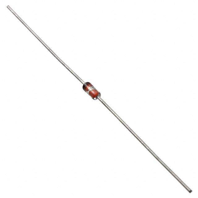
ICGOO电子元器件商城为您提供1N5359BRLG由ON Semiconductor设计生产,在icgoo商城现货销售,并且可以通过原厂、代理商等渠道进行代购。 1N5359BRLG价格参考。ON Semiconductor1N5359BRLG封装/规格:二极管 - 齐纳 - 单, Zener Diode 24V 5W ±5% Through Hole Axial。您可以下载1N5359BRLG参考资料、Datasheet数据手册功能说明书,资料中有1N5359BRLG 详细功能的应用电路图电压和使用方法及教程。
ON Semiconductor的1N5359BRLG是一款齐纳二极管,属于1N5300系列,标称齐纳电压为24V,功率为5W。该器件主要用于电压稳压和过压保护电路中。

典型应用场景包括:电源稳压电路,用于为敏感电子元件提供稳定的参考电压;在直流电源或充电系统中,防止电压波动对后级电路造成损害;工业控制设备、消费类电子产品及通信设备中的保护电路;也可用作电压钳位元件,在瞬态电压抑制(TVS)应用中保护半导体器件免受浪涌电压冲击。

由于其较高的功率耗散能力(5W),1N5357BRLG适用于需要承受短暂过载或高能量脉冲的场合。此外,该器件采用轴向封装(DO-13),具有良好的热稳定性和可靠性,适合在较宽温度范围(-65°C 至 +200°C)内工作,适用于严苛环境下的应用。

1N5359BRLG符合RoHS标准,无铅环保,广泛应用于汽车电子、电源适配器、电池管理系统(BMS)、工业电源模块等领域。其精准的电压调节能力和高稳定性,使其成为中等功率稳压与保护设计中的优选器件。
| 参数 | 数值 |
| 产品目录 | |
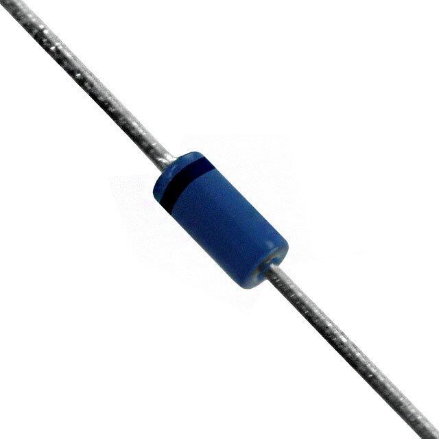
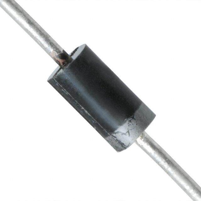
| 描述 | DIODE ZENER 24V 5W AXIAL稳压二极管 24V 5W |
| 产品分类 | 单二极管/齐纳分离式半导体 |
| 品牌 | ON Semiconductor |
| 产品手册 | |
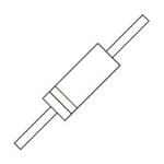
| 产品图片 |
|
| rohs | 符合RoHS无铅 / 符合限制有害物质指令(RoHS)规范要求 |
| 产品系列 | 二极管与整流器,稳压二极管,ON Semiconductor 1N5359BRLG- |
| 数据手册 | |
| 产品型号 | 1N5359BRLG |
| PCN设计/规格 | |
| 不同If时的电压-正向(Vf) | 1.2V @ 1A |
| 不同 Vr时的电流-反向漏电流 | 500nA @ 18.2V |
| 产品目录页面 | |
| 产品种类 | |
| 供应商器件封装 | 轴向 |
| 其它名称 | 1N5359BRLGOSCT |
| 功率-最大值 | 5W |
| 功率耗散 | 5 W |
| 包装 | 剪切带 (CT) |
| 商标 | ON Semiconductor |
| 安装类型 | 通孔 |
| 安装风格 | Through Hole |
| 容差 | ±5% |
| 封装 | Reel |
| 封装/外壳 | T-18,轴向 |
| 封装/箱体 | DO-35 |
| 工作温度 | -65°C ~ 200°C |
| 工厂包装数量 | 4000 |
| 最大反向漏泄电流 | 500 nA |
| 最大工作温度 | + 200 C |
| 最大齐纳阻抗 | 3.5 Ohms |
| 最小工作温度 | - 65 C |
| 标准包装 | 1 |
| 电压-齐纳(标称值)(Vz) | 24V |
| 电压容差 | 5 % |
| 电压调节准确度 | 550 mV |
| 系列 | 1N53 |
| 配置 | Single |
| 阻抗(最大值)(Zzt) | 3.5 欧姆 |
| 齐纳电压 | 24 V |
| 齐纳电流 | 198 mA |


- 商务部:美国ITC正式对集成电路等产品启动337调查
- 曝三星4nm工艺存在良率问题 高通将骁龙8 Gen1或转产台积电
- 太阳诱电将投资9.5亿元在常州建新厂生产MLCC 预计2023年完工
- 英特尔发布欧洲新工厂建设计划 深化IDM 2.0 战略
- 台积电先进制程称霸业界 有大客户加持明年业绩稳了
- 达到5530亿美元!SIA预计今年全球半导体销售额将创下新高
- 英特尔拟将自动驾驶子公司Mobileye上市 估值或超500亿美元
- 三星加码芯片和SET,合并消费电子和移动部门,撤换高东真等 CEO
- 三星电子宣布重大人事变动 还合并消费电子和移动部门
- 海关总署:前11个月进口集成电路产品价值2.52万亿元 增长14.8%


PDF Datasheet 数据手册内容提取
1N53 Series (cid:2) 5 Watt Surmetic 40 Zener Voltage Regulators This is a complete series of 5 Watt Zener diodes with tight limits and better operating characteristics that reflect the superior capabilities of silicon−oxide passivated junctions. All this in an axial lead, transfer−molded plastic package that offers protection in all common http://onsemi.com environmental conditions. Features Cathode Anode • Zener Voltage Range − 3.3 V to 200 V • ESD Rating of Class 3 (>16 kV) per Human Body Model • Surge Rating of up to 180 W @ 8.3 ms • Maximum Limits Guaranteed on up to Six Electrical Parameters • Pb−Free Packages are Available* AXIAL LEAD Mechanical Characteristics CASE 017AA PLASTIC CASE: Void free, transfer−molded, thermosetting plastic FINISH: All external surfaces are corrosion resistant and leads are readily solderable MAXIMUM LEAD TEMPERATURE FOR SOLDERING PURPOSES: MARKING DIAGRAM 260°C, 1/16 in. from the case for 10 seconds POLARITY: Cathode indicated by polarity band A MOUNTING POSITION: Any 1N 53xxB YYWW(cid:2) (cid:2) MAXIMUM RATINGS A = Assembly Location Rating Symbol Value Unit 1N53xxB = Device Number Max. Steady State Power Dissipation PD 5 W (Refer to Tables on Pages 3 & 4) @ TL = 25°C, Lead Length = 3/8 in YY = Year Derate above 25°C 40 mW/°C WW = Work Week (cid:2) = Pb−Free Package Junction−to−Lead Thermal Resistance (cid:2)JL 25 °C/W (Note: Microdot may be in either location) Operating and Storage TJ, Tstg −65 to +200 °C Temperature Range (Note 1) Stresses exceeding Maximum Ratings may damage the device. Maximum Ratings are stress ratings only. Functional operation above the Recommended ORDERING INFORMATION Operating Conditions is not implied. Extended exposure to stresses above the Recommended Operating Conditions may affect device reliability. Device Package Shipping† 1. Max operating temperature for DC conditions is 150°C, but not to exceed 200°C for pulsed conditions with low duty cycle or non−repetitive. 1N53xxB, G Axial Lead 1000 Units/Box (Pb−Free) 1N53xxBRL, G Axial Lead 4000/Tape & Reel (Pb−Free) †For information on tape and reel specifications, including part orientation and tape sizes, please refer to our Tape and Reel Packaging Specifications Brochure, BRD8011/D. *For additional information on our Pb−Free strategy and soldering details, please download the ON Semiconductor Soldering and Mounting Techniques Reference Manual, SOLDERRM/D. © Semiconductor Components Industries, LLC, 2013 1 Publication Order Number: November, 2013 − Rev. 15 1N5333B/D
1N53 Series ELECTRICAL CHARACTERISTICS (TA = 25°C unless I otherwise noted, VF = 1.2 V Max @ IF = 1.0 A for all types) Symbol Parameter IF VZ Reverse Zener Voltage @ IZT IZT Reverse Current ZZT Maximum Zener Impedance @ IZT VZVR V IZK Reverse Current IR VF ZZK Maximum Zener Impedance @ IZK IZT IR Reverse Leakage Current @ VR VR Breakdown Voltage IF Forward Current VF Forward Voltage @ IF IR Maximum Surge Current @ TA = 25°C Zener Voltage Regulator (cid:3)VZ Reverse Zener Voltage Change IZM Maximum DC Zener Current ELECTRICAL CHARACTERISTICS (TA = 25°C unless otherwise noted, VF = 1.2 V Max @ IF = 1.0 A for all types) Leakage Zener Voltage (Note 3) Zener Impedance (Note 3) Current IR (cid:2)VZ IZM Device† Device VZ (Volts) @ IZT ZZT @ IZT ZZK @ IZK IZK IR @ VR (Note 4) (Note 5) (Note 6) (Note 2) Marking Min Nom Max mA (cid:3) (cid:3) mA (cid:4)A Max Volts A Volts mA 1N5333B 1N5333B 3.14 3.3 3.47 380 3 400 1 300 1 20 0.85 1440 1N5334B 1N5334B 3.42 3.6 3.78 350 2.5 500 1 150 1 18.7 0.8 1320 1N5335B 1N5335B 3.71 3.9 4.10 320 2 500 1 50 1 17.6 0.54 1220 1N5336B 1N5336B 4.09 4.3 4.52 290 2 500 1 10 1 16.4 0.49 1100 1N5337B 1N5337B 4.47 4.7 4.94 260 2 450 1 5 1 15.3 0.44 1010 1N5338B 1N5338B 4.85 5.1 5.36 240 1.5 400 1 1 1 14.4 0.39 930 1N5339B 1N5339B 5.32 5.6 5.88 220 1 400 1 1 2 13.4 0.25 865 1N5340B 1N5340B 5.70 6.0 6.30 200 1 300 1 1 3 12.7 0.19 790 1N5341B 1N5341B 5.89 6.2 6.51 200 1 200 1 1 3 12.4 0.1 765 1N5342B 1N5342B 6.46 6.8 7.14 175 1 200 1 10 5.2 11.5 0.15 700 1N5343B 1N5343B 7.13 7.5 7.88 175 1.5 200 1 10 5.7 10.7 0.15 630 1N5344B 1N5344B 7.79 8.2 8.61 150 1.5 200 1 10 6.2 10 0.2 580 1N5345B 1N5345B 8.27 8.7 9.14 150 2 200 1 10 6.6 9.5 0.2 545 1N5346B 1N5346B 8.65 9.1 9.56 150 2 150 1 7.5 6.9 9.2 0.22 520 1N5347B 1N5347B 9.50 10 10.5 125 2 125 1 5 7.6 8.6 0.22 475 Devices listed in bold, italic are ON Semiconductor Preferred devices. Preferred devices are recommended choices for future use and best overall value. 2. TOLERANCE AND TYPE NUMBER DESIGNATION: The JEDEC type numbers shown indicate a tolerance of ±5%. 3. ZENER VOLTAGE (VZ) and IMPEDANCE (IZT and IZK): Test conditions for zener voltage and impedance are as follows: IZ is applied 40 ±10 ms prior to reading. Mounting contacts are located 3/8″ to 1/2″ from the inside edge of mounting clips to the body of the diode (TA = 25°C +8°C, −2°C). 4. SURGE CURRENT (IR): Surge current is specified as the maximum allowable peak, non−recurrent square−wave current with a pulse width, PW, of 8.3 ms. The data given in Figure 5 may be used to find the maximum surge current for a square wave of any pulse width between 1 ms and 1000 ms by plotting the applicable points on logarithmic paper. Examples of this, using the 3.3 V and 200 V zener are shown in Figure 6. Mounting contact located as specified in Note 2 (TA = 25°C +8°C, −2°C). 5. VOLTAGE REGULATION ((cid:2)VZ): The conditions for voltage regulation are as follows: VZ measurements are made at 10% and then at 50% of the IZ max value listed in the electrical characteristics table. The test current time duration for each VZ measurement is 40 ±10 ms. Mounting contact located as specified in Note 2 (TA = 25°C +8°C, −2°C). 6. MAXIMUM REGULATOR CURRENT (IZM): The maximum current shown is based on the maximum voltage of a 5% type unit, therefore, it applies only to the B−suffix device. The actual IZM for any device may not exceed the value of 5 watts divided by the actual VZ of the device. TL = 25°C at 3/8″ maximum from the device body. †The “G’’ suffix indicates Pb−Free package or Pb−Free packages are available. http://onsemi.com 2
1N53 Series ELECTRICAL CHARACTERISTICS (TA = 25°C unless otherwise noted, VF = 1.2 V Max @ IF = 1.0 A for all types) Leakage Zener Voltage (Note 8) Zener Impedance (Note 8) Current (cid:2)VZ IR (Note IZM Device† Device VZ (Volts) @ IZT ZZT @ IZT ZZK @ IZK IZK IR @ VR (Note 9) 10) (Note 11) (Note 7) Marking Min Nom Max mA (cid:3) (cid:3) mA (cid:4)A Max Volts A Volts mA 1N5348B 1N5348B 10.45 11 11.55 125 2.5 125 1 5 8.4 8.0 0.25 430 1N5349B 1N5349B 11.4 12 12.6 100 2.5 125 1 2 9.1 7.5 0.25 395 1N5350B 1N5350B 12.35 13 13.65 100 2.5 100 1 1 9.9 7.0 0.25 365 1N5351B 1N5351B 13.3 14 14.7 100 2.5 75 1 1 10.6 6.7 0.25 340 1N5352B 1N5352B 14.25 15 15.75 75 2.5 75 1 1 11.5 6.3 0.25 315 1N5353B 1N5353B 15.2 16 16.8 75 2.5 75 1 1 12.2 6.0 0.3 295 1N5354B 1N5354B 16.15 17 17.85 70 2.5 75 1 0.5 12.9 5.8 0.35 280 1N5355B 1N5355B 17.1 18 18.9 65 2.5 75 1 0.5 13.7 5.5 0.4 264 1N5356B 1N5356B 18.05 19 19.95 65 3 75 1 0.5 14.4 5.3 0.4 250 1N5357B 1N5357B 19 20 21 65 3 75 1 0.5 15.2 5.1 0.4 237 1N5358B 1N5358B 20.9 22 23.1 50 3.5 75 1 0.5 16.7 4.7 0.45 216 1N5359B 1N5359B 22.8 24 25.2 50 3.5 100 1 0.5 18.2 4.4 0.55 198 1N5360B 1N5360B 23.75 25 26.25 50 4 110 1 0.5 19 4.3 0.55 190 1N5361B 1N5361B 25.65 27 28.35 50 5 120 1 0.5 20.6 4.1 0.6 176 1N5362B 1N5362B 26.6 28 29.4 50 6 130 1 0.5 21.2 3.9 0.6 170 1N5363B 1N5363B 28.5 30 31.5 40 8 140 1 0.5 22.8 3.7 0.6 158 1N5364B 1N5364B 31.35 33 34.65 40 10 150 1 0.5 25.1 3.5 0.6 144 1N5365B 1N5365B 34.2 36 37.8 30 11 160 1 0.5 27.4 3.5 0.65 132 1N5366B 1N5366B 37.05 39 40.95 30 14 170 1 0.5 29.7 3.1 0.65 122 1N5367B 1N5367B 40.85 43 45.15 30 20 190 1 0.5 32.7 2.8 0.7 110 1N5368B 1N5368B 44.65 47 49.35 25 25 210 1 0.5 35.8 2.7 0.8 100 1N5369B 1N5369B 48.45 51 53.55 25 27 230 1 0.5 38.8 2.5 0.9 93 1N5370B 1N5370B 53.2 56 58.8 20 35 280 1 0.5 42.6 2.3 1.0 86 1N5371B 1N5371B 57 60 63 20 40 350 1 0.5 45.5 2.2 1.2 79 1N5372B 1N5372B 58.9 62 65.1 20 42 400 1 0.5 47.1 2.1 1.35 76 1N5373B 1N5373B 64.6 68 71.4 20 44 500 1 0.5 51.7 2.0 1.52 70 1N5374B 1N5374B 71.25 75 78.75 20 45 620 1 0.5 56 1.9 1.6 63 1N5375B 1N5375B 77.9 82 86.1 15 65 720 1 0.5 62.2 1.8 1.8 58 1N5377B 1N5377B 86.45 91 95.55 15 75 760 1 0.5 69.2 1.6 2.2 52.5 1N5378B 1N5378B 95 100 105 12 90 800 1 0.5 76 1.5 2.5 47.5 1N5380B 1N5380B 114 120 126 10 170 1150 1 0.5 91.2 1.3 2.5 39.5 1N5381B 1N5381B 123.5 130 136.5 10 190 1250 1 0.5 98.8 1.2 2.5 36.6 1N5383B 1N5383B 142.5 150 157.5 8 330 1500 1 0.5 114 1.1 3.0 31.6 1N5384B 1N5384B 152 160 168 8 350 1650 1 0.5 122 1.1 3.0 29.4 1N5386B 1N5386B 171 180 189 5 430 1750 1 0.5 137 1.0 4.0 26.4 1N5387B 1N5387B 180.5 190 199.5 5 450 1850 1 0.5 144 0.9 5.0 25 1N5388B 1N5388B 190 200 210 5 480 1850 1 0.5 152 0.9 5.0 23.6 Devices listed in bold, italic are ON Semiconductor Preferred devices. Preferred devices are recommended choices for future use and best overall value. 7. TOLERANCE AND TYPE NUMBER DESIGNATION: The JEDEC type numbers shown indicate a tolerance of ±5%. 8. ZENER VOLTAGE (VZ) and IMPEDANCE (IZT and IZK): Test conditions for zener voltage and impedance are as follows: IZ is applied 40 ±10 ms prior to reading. Mounting contacts are located 3/8″ to 1/2″ from the inside edge of mounting clips to the body of the diode (TA = 25°C +8°C, −2°C). 9. SURGE CURRENT (IR): Surge current is specified as the maximum allowable peak, non−recurrent square−wave current with a pulse width, PW, of 8.3 ms. The data given in Figure 5 may be used to find the maximum surge current for a square wave of any pulse width between 1 ms and 1000 ms by plotting the applicable points on logarithmic paper. Examples of this, using the 3.3 V and 200 V zener are shown in Figure 6. Mounting contact located as specified in Note 7 (TA = 25°C +8°C, −2°C). 10.VOLTAGE REGULATION ((cid:2)VZ): The conditions for voltage regulation are as follows: VZ measurements are made at 10% and then at 50% of the IZ max value listed in the electrical characteristics table. The test current time duration for each VZ measurement is 40 ±10 ms. Mounting contact located as specified in Note 7 (TA = 25°C +8°C, −2°C). 11.MAXIMUM REGULATOR CURRENT (IZM): The maximum current shown is based on the maximum voltage of a 5% type unit, therefore, it applies only to the B−suffix device. The actual IZM for any device may not exceed the value of 5 watts divided by the actual VZ of the device. TL = 25°C at 3/8″ maximum from the device body. †The “G’’ suffix indicates Pb−Free package or Pb−Free packages are available. http://onsemi.com 3
1N53 Series W) C/ 40 °E ( C N A ST 30 SI E R L A M R 20 E H T L L D A E O‐L 10 T N‐ EQUAL CONDUCTION O THROUGH EACH LEAD TI NC 0 U 0 0.2 0.4 0.6 0.8 1 J , L L, LEAD LENGTH TO HEATSINK (INCH) J θ Figure 1. Typical Thermal Resistance TEMPERATURE COEFFICIENTS T 10 N E CI 8 FI F COE ZT 6 RE @ I 4 TUC) RA°V/ 2 MPE(m RANGE E 0 T V, Z -2 θ 3 4 5 6 7 8 9 10 VZ, ZENER VOLTAGE @ IZT (VOLTS) Figure 2. Temperature Coefficient-Range for Units 3 to 10 Volts 300 T N E 200 CI FI F 100 E RE CO@ IZT 50 RANGE TUC) 30 RA°V/ 20 Em MP( E 10 T , Z V 5 θ 0 20 40 60 80 100 120 140 160 180 200 220 VZ, ZENER VOLTAGE @ IZT (VOLTS) Figure 3. Temperature Coefficient-Range for Units 10 to 220 Volts http://onsemi.com 4
1N53 Series 100 E C N A ST 0.5 ESIW) 10 0.2 MAL R°D (C/ 0.1 RA 0.05 HELE 1 (t, D), TRANSIENT TJUNCTION‐TO‐ 0.1 00D.. 00=12 0 PPK t1 t2 REPETI(cid:2)TSJILIVN(EtG,D PL)[UE w= L hPDSeUD Er*eLU S(cid:2) ST(cid:2) J(cid:3)EJLYL (T(cid:3)(C∞tJ) YT)L i+ sJC=(L 1D L (cid:2)=−E J= DL,(cid:2) ()DJ0t L,* Dc( =t(cid:2)u)) JPPtr1LvPP/(ettKK2)] L 0.01 J θ 0.0000001 0.000001 0.00001 0.0001 0.001 0.01 0.1 1 10 100 t, TIME (SECONDS) Figure 4. Typical Thermal Response L, Lead Length = 3/8 Inch 40 30 20 S) 20 S) MP PW(cid:3)=(cid:3)1(cid:3)ms* MP 10 ENT (A 10 PW(cid:3)=(cid:3)8.3(cid:3)ms* ENT (A 5 VZ(cid:3)=(cid:3)3.3(cid:3)V RR 4 RR U U E C 2 E C 2 G G UR 1 UR 1 S S K K I, PEAr00..24 *SQUARE WAVE PW(cid:3)=(cid:3)100(cid:3)ms* I, PEAr00..25 PLOTTED FROM INFORMATION VZ(cid:3)=(cid:3)200(cid:3)V PW(cid:3)=(cid:3)1000(cid:3)ms* GIVEN IN FIGURE 5 0.1 0.1 3 4 6 8 10 20 30 40 60 80 100 200 1 10 100 1000 NOMINAL VZ (V) PW, PULSE WIDTH (ms) Figure 5. Maximum Non-Repetitive Surge Current Figure 6. Peak Surge Current versus Pulse Width versus Nominal Zener Voltage (See Note 4) (See Note 4) 1000 T(cid:3)=(cid:3)25°C T(cid:3)=(cid:3)25°C 1000 TC(cid:3)=(cid:3)25°C A) 100 m mA) T ( NT (100 REN RE UR 10 R C CU 10 ER R N E E EN , Z 1 , Z 1 IZ Z I 0.1 0.1 1 2 3 4 5 6 7 8 9 10 10 20 30 40 50 60 70 80 VZ, ZENER VOLTAGE (VOLTS) VZ, ZENER VOLTAGE (VOLTS) Figure 7. Zener Voltage versus Zener Current Figure 8. Zener Voltage versus Zener Current V =3.3 thru 10 Volts V = 11 thru 75 Volts Z Z http://onsemi.com 5
1N53 Series A) 100 m T ( N E R UR 10 C R E N E Z , 1 Z I 0.1 80 100 120 140 160 180 200 220 VZ, ZENER VOLTAGE (VOLTS) Figure 9. Zener Voltage versus Zener Current V = 82 thru 200 Volts Z APPLICATION NOTE Since the actual voltage available from a given Zener For worst-case design, using expected limits of I , limits Z diode is temperature dependent, it is necessary to determine of P and the extremes of T ((cid:3)T ) may be estimated. D J J junction temperature under any set of operating conditions Changes in voltage, V , can then be found from: Z in order to calculate its value. The following procedure is (cid:3)V = (cid:2) (cid:3)T VZ J recommended: (cid:2) , the Zener voltage temperature coefficient, is found Lead Temperature, T , should be determined from: VZ L from Figures 2 and 3. T = (cid:2) P + T L LA D A Under high power-pulse operation, the Zener voltage will (cid:2) is the lead-to-ambient thermal resistance and P is the LA D vary with time and may also be affected significantly by the power dissipation. zener resistance. For best regulation, keep current Junction Temperature, T , may be found from: J excursions as low as possible. T = T + (cid:3)T Data of Figure 4 should not be used to compute surge J L JL (cid:3)T is the increase in junction temperature above the lead capability. Surge limitations are given in Figure 5. They are JL lower than would be expected by considering only junction temperature and may be found from Figure 4 for a train of temperature, as current crowding effects cause temperatures power pulses or from Figure 1 for dc power. to be extremely high in small spots resulting in device (cid:3)T = (cid:2) P JL JL D degradation should the limits of Figure 5 be exceeded. http://onsemi.com 6
1N53 Series PACKAGE DIMENSIONS SURMETIC 40, AXIAL LEAD CASE 017AA ISSUE O NOTES: 1. CONTROLLING DIMENSION: INCH 2. LEAD DIAMETER AND FINISH NOT CONTROLLED WITHIN DIMENSION F. B 3. CATHODE BAND INDICATES POLARITY INCHES MILLIMETERS DIM MIN MAX MIN MAX D A 0.330 0.350 8.38 8.89 K B 0.130 0.145 3.30 3.68 D 0.037 0.043 0.94 1.09 F F --- 0.050 --- 1.27 K 1.000 1.250 25.40 31.75 A F K SURMETIC is a trademark of Semiconductor Components Industries, LLC (SCILLC). ON Semiconductor and are registered trademarks of Semiconductor Components Industries, LLC (SCILLC). SCILLC reserves the right to make changes without further notice to any products herein. SCILLC makes no warranty, representation or guarantee regarding the suitability of its products for any particular purpose, nor does SCILLC assume any liability arising out of the application or use of any product or circuit, and specifically disclaims any and all liability, including without limitation special, consequential or incidental damages. “Typical” parameters which may be provided in SCILLC data sheets and/or specifications can and do vary in different applications and actual performance may vary over time. All operating parameters, including “Typicals” must be validated for each customer application by customer’s technical experts. SCILLC does not convey any license under its patent rights nor the rights of others. SCILLC products are not designed, intended, or authorized for use as components in systems intended for surgical implant into the body, or other applications intended to support or sustain life, or for any other application in which the failure of the SCILLC product could create a situation where personal injury or death may occur. Should Buyer purchase or use SCILLC products for any such unintended or unauthorized application, Buyer shall indemnify and hold SCILLC and its officers, employees, subsidiaries, affiliates, and distributors harmless against all claims, costs, damages, and expenses, and reasonable attorney fees arising out of, directly or indirectly, any claim of personal injury or death associated with such unintended or unauthorized use, even if such claim alleges that SCILLC was negligent regarding the design or manufacture of the part. SCILLC is an Equal Opportunity/Affirmative Action Employer. This literature is subject to all applicable copyright laws and is not for resale in any manner. PUBLICATION ORDERING INFORMATION LITERATURE FULFILLMENT: N. American Technical Support: 800−282−9855 Toll Free ON Semiconductor Website: www.onsemi.com Literature Distribution Center for ON Semiconductor USA/Canada P.O. Box 5163, Denver, Colorado 80217 USA Europe, Middle East and Africa Technical Support: Order Literature: http://www.onsemi.com/orderlit Phone: 303−675−2175 or 800−344−3860 Toll Free USA/Canada Phone: 421 33 790 2910 Fax: 303−675−2176 or 800−344−3867 Toll Free USA/Canada Japan Customer Focus Center For additional information, please contact your local Email: orderlit@onsemi.com Phone: 81−3−5817−1050 Sales Representative http://onsemi.com 1N5333B/D 7
Mouser Electronics Authorized Distributor Click to View Pricing, Inventory, Delivery & Lifecycle Information: O N Semiconductor: 1N5387BRLG 1N5333B 1N5333BG 1N5333BRL 1N5333BRLG 1N5334B 1N5334BG 1N5334BRL 1N5334BRLG 1N5335B 1N5335BG 1N5335BRL 1N5335BRLG 1N5336B 1N5336BG 1N5336BRL 1N5336BRLG 1N5337B 1N5337BG 1N5337BRL 1N5337BRLG 1N5338B 1N5338BG 1N5338BRL 1N5338BRLG 1N5339B 1N5339BG 1N5339BRL 1N5339BRLG 1N5340B 1N5340BG 1N5340BRL 1N5340BRLG 1N5341B 1N5341BG 1N5341BRL 1N5341BRLG 1N5342B 1N5342BG 1N5342BRL 1N5342BRLG 1N5343B 1N5343BG 1N5343BRL 1N5343BRLG 1N5344B 1N5344BG 1N5344BRL 1N5344BRLG 1N5345B 1N5345BRL 1N5345BRLG 1N5346B 1N5346BG 1N5346BRL 1N5346BRLG 1N5347B 1N5347BG 1N5347BRL 1N5347BRLG 1N5348B 1N5348BG 1N5348BRL 1N5348BRLG 1N5349B 1N5349BG 1N5349BRL 1N5349BRLG 1N5350B 1N5350BG 1N5350BRL 1N5350BRLG 1N5351B 1N5351BG 1N5351BRL 1N5351BRLG 1N5352B 1N5352BG 1N5352BRL 1N5352BRLG 1N5353B 1N5353BG 1N5353BRL 1N5353BRLG 1N5354B 1N5354BG 1N5354BRL 1N5354BRLG 1N5355B 1N5355BG 1N5355BRL 1N5355BRLG 1N5356B 1N5356BG 1N5356BRL 1N5356BRLG 1N5357B 1N5357BG 1N5357BRL 1N5357BRLG