ICGOO在线商城 > 1583N16-U

 Datasheet下载
- 型号: 1583N16-U
- 制造商: THAT Corporation
- 库位|库存: xxxx|xxxx
- 要求:
| 数量阶梯 | 香港交货 | 国内含税 |
| +xxxx | $xxxx | ¥xxxx |
查看当月历史价格
查看今年历史价格
1583N16-U产品简介:
ICGOO电子元器件商城为您提供1583N16-U由THAT Corporation设计生产,在icgoo商城现货销售,并且可以通过原厂、代理商等渠道进行代购。 提供1583N16-U价格参考以及THAT Corporation1583N16-U封装/规格参数等产品信息。 你可以下载1583N16-U参考资料、Datasheet数据手册功能说明书, 资料中有1583N16-U详细功能的应用电路图电压和使用方法及教程。
| 参数 | 数值 |
| 品牌 | THAT |
| 产品目录 | 半导体 |
| 描述 | 传声器前置放大器 Lw-Noise Differntial Audio Preamp IC |
| 产品分类 | 集成电路 - IC |
| 产品手册 | |
| 产品图片 |
|
| rohs | 符合RoHS |
| 产品系列 | 音频 IC,传声器前置放大器,THAT 1583N16-U |
| 产品型号 | 1583N16-U |
| THD+噪声 | 0.006 % |
| 产品种类 | 传声器前置放大器 |
| 可用增益调整 | 0 dB to 60 dB |
| 商标 | THAT |
| 安装风格 | SMD/SMT |
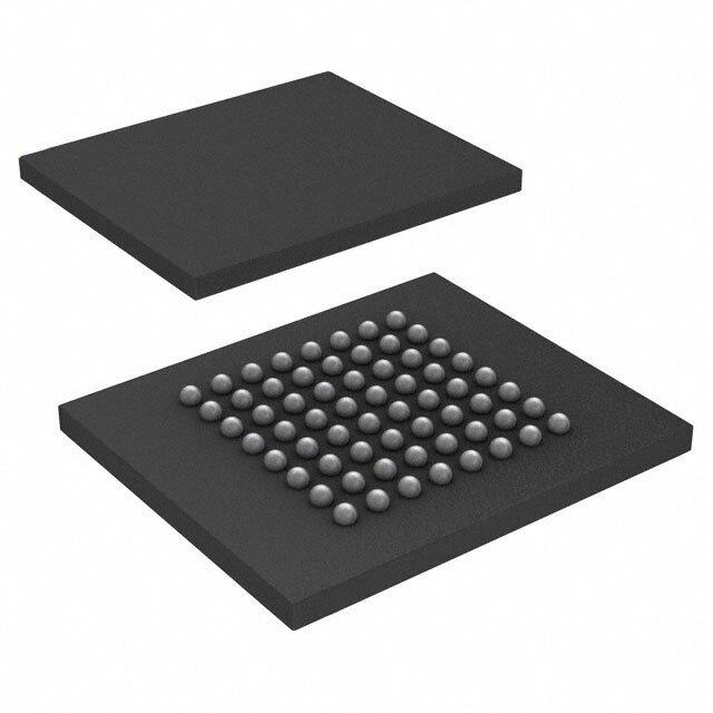
| 封装 | Tube |
| 封装/箱体 | QFN-16 |
| 工作温度范围 | - 40 C to + 85 C |
| 工作电源电压 | 5 V to 18 V |
| 工厂包装数量 | 92 |
| 最大工作温度 | + 85 C |
| 最小工作温度 | - 40 C |
| 电源电压-最大 | 18 V |
| 电源电压-最小 | 5 V |
| 电源电流 | 7 mA |
| 输入电压范围—最大 | 18 V |
| 输入补偿电压 | 400 uV |


- 商务部:美国ITC正式对集成电路等产品启动337调查
- 曝三星4nm工艺存在良率问题 高通将骁龙8 Gen1或转产台积电
- 太阳诱电将投资9.5亿元在常州建新厂生产MLCC 预计2023年完工
- 英特尔发布欧洲新工厂建设计划 深化IDM 2.0 战略
- 台积电先进制程称霸业界 有大客户加持明年业绩稳了
- 达到5530亿美元!SIA预计今年全球半导体销售额将创下新高
- 英特尔拟将自动驾驶子公司Mobileye上市 估值或超500亿美元
- 三星加码芯片和SET,合并消费电子和移动部门,撤换高东真等 CEO
- 三星电子宣布重大人事变动 还合并消费电子和移动部门
- 海关总署:前11个月进口集成电路产品价值2.52万亿元 增长14.8%


PDF Datasheet 数据手册内容提取
Low-Noise, Differential Audio Preamplifier IC THAT1583 FEATURES APPLICATIONS • Low Noise: • Microphone Preamplifiers -128.9dBu (1.9nV/√Hz) EIN@60dB gain • Low THD+N: • Digitally-Controlled Microphone 0.001% ≤ 40 dB gain Preamplifiers 0.006% @ 60 dB gain • Differential Low-Noise Preamplifiers • Low Current: 7.0 mA typ • Differential Summing Amplifiers • Wide Bandwidth: 1.7MHz @40dB gain • Differential Variable-Gain Amplifiers • High Slew Rate: 50 V/µs • Wide Output Signal Swing: > +28dBu • Moving-Coil Transducer Amplifiers • Gain adjustable from 0 to >60 dB • Line Input Stages • Differential output • Audio • Small 4 x 4mm QFN16 package • Sonar • Mates with THAT's family of Digital • Instrumentation Preamplifier Controller ICs Description The THAT 1583 is a versatile, high performance optimize the output differential amplifier to suit current-feedback amplifier suitable for differential the specific application. microphone preamplifier and bus summing In analog variable-gain applications the part applications. It improves on previous, traditional supports the traditional approach using fixed R current-feedback designs (viz. THAT's 1510 & A and R and a single-section variable element for 1512) by offering a more versatile configuration B R . But, it also supports a dual-element alternative that can yield lower noise at low gains, lower G that offers improved performance. distortion overall, and higher slew rate. In addition to analog-controlled applications, the Amplifier gain is determined by three external 1583 is designed to mate perfectly with THAT's resistors (RA, RB, and RG). This makes it possible to series of Digital Preamplifier Controller ICs to optimize noise and bandwidth over a wide range of produce an optimized, digitally controlled gains, as well as optimize the taper of gain vs. preamplifier. rotation in variable-gain, pot-controlled applications. The 1583 operates from as little as ±5 V up The 1583's differential output simplifies connec- through ±18 V supplies. It accepts greater than tions to differential input devices such as A/D +28 dBu input signals at unity gain when converters. When required, designers are free to operated from ±18V supplies. Pin Name QFN Pin N/C* 1 OUT2 2 OUT1 3 N/C* 4 N/C* 5 Rg1 6 IN1 7 N/C* 8 N/C* 9 IN2 10 N/C* 11 V- 12 V+ 13 N/C* 14 Rg2 15 N/C* 16 V- Thermal Pad Figure 1. THAT1583 Block Diagram Table 1. Pin Assignments * N/C pins should be left open and not connected to other traces on the PCB THAT Corporation; 45 Sumner Street; Milford, Massachusetts 01757-1656; USA Tel: +1 508 478-9200; Fax +1 508 478-0990; Web: www.thatcorp.com Copyright © 2016, THAT Corporation; Doc 600173 Rev 03
THAT 1583 Low-Noise Page 2 of 16 Document 600173 Rev 03 Differential Audio Preamplifier IC SPECIFICATIONS1 Absolute Maximum Ratings2 Supply Voltage (V+) - (V-) 40 V Operating Temperature Range (T ) -40 to +85 ºC OP Maximum Input Voltage (V ) (V+) +0.5V to (V-)-0.5V Junction Temperature (T ) +125 ºC IMax JMAX Storage Temperature Range (T ) -40 to +125 ºC Output Short-Circuit Duration, STG between outputs and/or GND (t ) Continuous SH Electrical Characteristics3,4,5 Parameter Symbol Conditions Min Typ Max Units Power Supply Supply Voltage V+; - (V-) Referenced to GND 5 — 18 V Supply Current I+; -(I-) No Signal — 7.0 10 mA Input Characteristics Input Bias Current I No signal; either input connected to GND — 2.0 4.4 µA B Input Offset Current I No signal -440 — +440 nA B-OFF R Input Bias Current I No signal -20 +2 +20 µA G BRG R Input Offset Current I No signal -4.5 — +4.5 µA G BRG-OFF Differential Input Offset Voltage V No signal, Includes I * R OS BRG-OFF G 0 dB gain -15 — +15 mV +60 dB gain -450 — +450 µV Input Common Mode Voltage Range V Common Mode (V-) + 1.5 — (V+) -4 V IN_CM Maximum Differential Input Level V R = ∞ — 26.4 — dBu IN-BAL G Supply Voltage ±18V — 28.0 — dBu Output Characteristics Differential Output Offset G = gain -(15 + 0.45*G) — (15 + 0.45*G) mV Common Mode Output Voltage V No signal; — -630 — mV OSCM IN1, IN2 connected to GND Maximum Single Output Voltage V G=20dB, R= 2 kΩ (V-) + 1.2 — (V+) - 2 V OUT-SINGLE L Differential Short Circuit Current I R = 0 Ω — ± 70 — mA SC L Maximum Capacitive Load C Over entire temperature range — — 30 pF L MAX Stable operation 30% overshoot — 75 — pF Maximum Differential Output Level V R= 2 kΩ 28 — — dBu OUT L Gain > 2 dB 1. All specifications are subject to change without notice. 2. Stresses above those listed under "Absolute Maximum Ratings" may cause permanent damage to the device. These are stress ratings only; the functional operation of the device at these or any other conditions above those indicated in the operational sections of this specification is not implied. Exposure to absolute maximum rating conditions for extended periods may affect device reliability. 3. Unless otherwise noted, TA = 25ºC, V+ = +15V, V- = -15V. 4. 0 dBu = 0.775 Vrms 5. Unless otherwise noted, feedback resistors = 2.21 kΩ; CL = 10 pF. Circuit is as shown in Figure 15. THAT Corporation; 45 Sumner Street; Milford, Massachusetts 01757-1656; USA Tel: +1 508 478-9200; Fax +1 508 478-0990; Web: www.thatcorp.com Copyright © 2016, THAT Corporation; All rights reserved.
THAT 1583 Low-Noise Page 3 of 16 Document 600173 Rev 03 Differential Audio Preamplifier IC Electrical Characteristics (con’t) 3,4,5 Parameter Symbol Conditions Min. Typ. Max Units AC Characteristics Feedback Impedance R = R Refer to Figure 15 2 — — kΩ A B Differential Gain A Programmed by R , R , R 0 — 70 dB V A B G Refer to Figure 15 Power Supply Rejection Ratio PSRR V+ = -(V-); ±5V to ±18V 0 dB gain — 105 — dB 20 dB gain — 116 — dB 40 dB gain — 140 — dB 60 dB gain — 140 — dB Bandwidth -3dB f Small signal; R =R =2.21kΩ; Refer to Figure 5 -3dB A B 0 dB gain — 14 — MHz 20 dB gain — 9 — MHz 40 dB gain — 1.7 — MHz 60 dB gain — 192 — kHz Small signal; R =∞ (0 dB gain) G R = R = 2 kΩ — 16 — MHz A B R = R = 5 kΩ — 4 — MHz A B R = R = 10 kΩ — 1.6 — MHz A B Slew Rate SR V = 10V ; R=2kΩ OUT P-P L C=30pF; G=20dB — 50 — V/µs L Total Harmonic Distortion + Noise THD + N V = 5V ; R=2kΩ; f=1kHz; BW=22kHz OUT RMS L 0 dB gain — 0.0006 — % 20 dB gain — 0.0008 — % 40 dB gain — 0.001 — % 60 dB gain — 0.006 — % Equivalent Input Noise Voltage e Inputs connected to GND; f=1kHz N R = R = 2.21kΩ; Refer to Figure 15 A B 0 dB gain — 40 — nV/√Hz 20 dB gain — 5.7 — nV/√Hz 40 dB gain — 2.3 — nV/√Hz 60 dB gain — 1.9 — nV/√Hz BW = 22kHz 60 dB gain — -128.9 — dBu A - weighted ; BW = 22kHz 60 dB gain — -131.2 — dBu Inputs connected to 150Ω; BW = 22kHz 60 dB gain — -126.5 — dBu Inputs connected to 150Ω; A - weighted 60 dB gain — -129.3 — dBu Equivalent Input Noise Current i f = 1kHz; 60 dB gain — 0.8 — pA/√Hz N Noise Figure NF 60 dB gain; Source impedance = 150 Ω — 3.9 — dB [dBu] -100 [dBu] -100 RS = 150 -105 -105 -110 -110 -115 -115 BW: 22Hz - 22kHz -120 -120 BW: A-weighted -125 -125 [dB] -130 [dB] -130 0 10 20 30 40 50 60 0 10 20 30 40 50 60 Figure 2. Equivalent Input Noise vs Gain and Figure 3. Equivalent Input Noise vs Gain and Bandwidth, Source Impedance; BW: 22Hz to 22kHz Source Impedance 150Ω THAT Corporation; 45 Sumner Street; Milford, Massachusetts 01757-1656; USA Tel: +1 508 478-9200; Fax +1 508 478-0990; Web: www.thatcorp.com Copyright © 2016, THAT Corporation; All rights reserved.
THAT 1583 Low-Noise Page 4 of 16 Document 600173 Rev 03 Differential Audio Preamplifier IC [dBu] [MHz] -90 10 -95 RA=RB=2k21 -100 -105 RA=RB=5k -110 1 RA=RB=10k -115 -120 -125 -130 [dB] 0.1 [dB] 0 10 20 30 40 50 60 0 10 20 30 40 50 60 Figure 4. Equivalent Input Noise vs Gain and Figure 5. Bandwidth vs Gain and Feedback Impedance Feedback Impedance; BW: 22Hz to 22kHz [%] [%] 0.1 0.1 60dB 0.01 0.01 50dB 60dB 40dB 30dB 50dB 0.001 0.001 20dB 40dB 10dB 30dB 0dB 10dB 20dB 0.0001 [dBu] 0.0001 [Hz] 0 5 10 15 20 25 30 100 1k 10k 20k Figure 6. THD+ Noise vs Level Figure 7. THD + Noise vs Frequency; Vout = 27dBu, RL = 10kΩ [V] [dB] 15 140 40 dB VOUTP 10 120 5 100 0 dB 80 0 60 -5 40 -10 VOUTN 20 [mA] -15 0 [Hz] 0 10 20 30 40 50 60 70 20 200 2k 20k 200k Figure 8. Power Supply Rejection vs Frequency Figure 9. Maximum Output Voltage vs Output Current THAT Corporation; 45 Sumner Street; Milford, Massachusetts 01757-1656; USA Tel: +1 508 478-9200; Fax +1 508 478-0990; Web: www.thatcorp.com Copyright © 2016, THAT Corporation; All rights reserved.
THAT 1583 Low-Noise Page 5 of 16 Document 600173 Rev 03 Differential Audio Preamplifier IC [mV] -20 -15 -10 -5 0 5 10 15 20 Figure 11. Representative Output Offset Voltage Figure 10. Maximum Output Level vs. Supply Voltage Distribution, 0dB Gain [uV] [uA] -800 -600 -400 -200 0 200 400 600 800 -30 -25 -20 -15 -10 -5 0 5 10 15 20 25 30 Figure 12. Representative Input Offset Voltage Figure 13. Representative R Input Bias G Distribution, 60dB Gain Current Distribution [uA] -5 -4 -3 -2 -1 0 1 2 3 4 5 Figure 14. Representative R Input Offset G Current Distribution THAT Corporation; 45 Sumner Street; Milford, Massachusetts 01757-1656; USA Tel: +1 508 478-9200; Fax +1 508 478-0990; Web: www.thatcorp.com Copyright © 2016, THAT Corporation; All rights reserved.
THAT 1583 Low-Noise Page 6 of 16 Document 600173 Rev 03 Differential Audio Preamplifier IC Theory of Operation Amplifier Overview Referring to Figure 15, the THAT1583's differential RA voltage gain (G) is set by the feedback resistors (R A and R ) and R , as shown in the following equation. B G The amplifier's minimum gain is unity (0 dB), which occurs with infinite R . The feedback resistors G should nominally be equal, though tight tolerance IN1 OUT+ matching is not r(cid:5)eq(cid:6)u+ire(cid:5)d.(cid:7) RM R1 RRGG12 OOUUTT12 OUT- (cid:1) = 1+ RG (cid:5) IN2 (cid:8) R2 In low-noise current-feedback amplifiers like the 1583, many performance characteristics depend RB critically on the impedance of the feedback network (R , R , and R ). A B G The 1583 (and 1570) offers a novel approach to an Figure 15. Simple THAT1583 Amplifier Circuit integrated microphone preamplifier in that all three gain resistors are external. This gives the designer noise will be the largest contributor. However, at freedom to select the optimal values for the best 1.9 nV/√Hz (-128.9 dBu unweighted, 22 kHz noise performance at the desired gain setting(s). bandwidth) the amplifier's own input noise is only 1.5 dB higher than that of a 150 Ω microphone (- Noise versus Gain 130.4 dBu). So, the external source impedance R is M a significant contributor to the total noise of the The noise performance of a preamplifier based on system. the 1583 is determined as the sum of several noise sources. These are as follows (refer to Figure 15 for At low gains (under about 20 dB), the dominant component reference designators): noise sources are factors 2 and 5. An important case occurs at 0 dB (unity) differential gain. In order to 1. the amplifier's own input voltage noise; reach 0 dB gain, RG is open (infinite resistance). In 2. the voltage noise of the gain-setting resistor this case, the current noise in RG1 and RG2 is drawn across the highest possible impedance (R and R network (R in parallel with R and R ); A B 3. the voltage Gnoise of the externaAl sourcBe im- alone, without any shunting effect of RG). The only way to mitigate this noise is to use lower values for pedance, connected to the 1583's input (R in M R and R . parallel with R + R ):, A B 1 2 4. the current noise from IN+ and IN-, developed Of course, there is a continuum of relative impor- across the source impedance (RM in parallel tances here as gain goes from minimum (0 dB) to with R1+R2), and maximum (over 70 dB). As gain varies, the im- 5. the current noise from RG1 and RG2, translated portance of each factor will vary in its own way, each to a voltage when drawn across the equivalent contributing a different relative amount to the total. impedance of the external gain-setting resistor In general, to minimize low-gain noise, we suggest to network (RG in parallel with RA and RB). keep RA and RB as small as possible. Since all these sources are uncorrelated, mostly Another perspective on noise performance is gained random (Gaussian) noise, these sources all add in by measuring the noise using an A-weighting filter. root-mean-square fashion. But which one is most Figure 3 compares equivalent input noise for various important changes with gain, so predicting how noise gains in a 22 kHz bandwidth vs. using an A-weighting varies can be complex. filter. The A-weighting filter improves input noise A complete discussion of these sources and their performance by about 3 dB. interaction is beyond the scope of this data sheet. For more information, see "De-Integrating Integrated Bandwidth Circuit Preamps", available from THAT Corporation's web site, especially pages 13 through 20 However, An important characteristic of current-feedback the following discussion covers the highlights. amplifiers is that the amplifier bandwidth is inversely At high gains (above 40 dB or so), the system noise proportional to the feedback resistance R and R . A B is typically dominated by the first three factors in the The bandwidth decreases with increasing feedback above list. At high gains, for practical values of RA, resistance. As mentioned before, the minimum value RB, and RG (where RG is typically less 100Ω) and of RA and RB is determined by the amplifier's stability typical external source impedances (microphones are and cannot be under any condition lower than 2 kΩ. generally around 150Ω), the amplifier's input voltage Figure 5 shows typical bandwidth versus gain for a few selected values of feedback resistance. THAT Corporation; 45 Sumner Street; Milford, Massachusetts 01757-1656; USA Tel: +1 508 478-9200; Fax +1 508 478-0990; Web: www.thatcorp.com Copyright © 2016, THAT Corporation; All rights reserved.
THAT 1583 Low-Noise Page 7 of 16 Document 600173 Rev 03 Differential Audio Preamplifier IC Note that the widest bandwidth may not always be the optimum condition. In digitally controlled applications using CMOS switches to vary gain, high RA bandwidth may allow charge injected by the switches to be amplified and sharp voltage spikes to appear at the output. Lower bandwidth can reduce this effect. Common Mode Gain IN1 OUT+ CG The amplifier common-mode gain is always unity RM R1 RG1 OUT1 (0 dB), regardless of the differential gain. So, any RG2 OUT2 OUT- common-mode input signal, along with the amplifi- RG IN2 er's own common-mode dc offset, will be transferred faithfully without gain or attenuation to the output. R2 The common-mode rejection ratio (CMRR) of the part RB will equal the differential gain, since differential signals are amplified while common-mode signals are not. The largest impact of significant common-mode signals is to limit 1583's dynamic range, since they Figure 16. Simple THAT1583 Circuit with CG can cause premature clipping of the input and outputs. The same will be true for subsequent stages. The 1583 output has a typical dc common mode offset of about -600 mV. This constrains output headroom on negative signal peaks by 600 mV. At Note that the R -C network forms a high-pass high power supplies, the 600 mV reduction of output G G filter. The high-pass filter's -3 dB corner frequency is swing may not matter. However, it has a more determined by the following equation. significant effect at the minimum power supply. If desired, a common-mode servo amplifier can be 1 added to drive the outputs' common-mode voltage to (cid:9) = 0 V by lifting the inputs' bias to approximately (cid:10) 2(cid:12)(cid:5) (cid:13) (cid:8) (cid:8) +600 mV. Note that it is more important to adjust the output to zero bias than the input, because the 1583's input voltage range is typically less than that Note that the cutoff varies with R and therefore for its output. G with gain. It is highest with lowest R (which occurs G Limiting Differential dc Gain at the highest gain). This can be a desirable effect in that at high gains it can significantly reduce the low In the circuit of Figure 15, the amplifier's differen- frequency rumble and noise from wind or micro- tial gain (G) extends to dc. As a result, the differential phone handling. dc offset at the outputs will vary with gain. This can Consider the circuits shown in Figure 17, which produce audible "thumps" when gain is varied has a fixed and variable R (R and R ). At quickly, and can produce significant and undesirable G GF GV maximum gain (60 dB), R = 10 Ω. With output dc offset at maximum gain. Any such offset G C = 3,300 µF, the high-pass corner frequency is will reduce the output voltage swing. G approximately 5 Hz. But, at minimum gain (6 dB), To see how important this is, suppose a particular R = 10kΩ. This drives the cutoff down to 0.005 Hz. G 1583 has an input offset of 400 µV and an output It may well be acceptable to reduce C by a factor of G offset of 10 mV. The output offset of that part would 10, to 330 µF. In this case the high-pass corner be 10.4 mV at unity (0 dB) gain. But, at 60 dB gain, would vary from 50 Hz at 60 dB gain to 0.05 Hz at the output dc offset will be 410 mV. If the gain is 6 dB gain. varied quickly, this ~400 mV dc shift will be audible. The dc voltage appearing across C is very small, G This issue can be addressed by ac coupling R as less than 450 mV, though its polarity will vary from G shown in Figure 16 with capacitor C . The capacitor sample to sample. C is usually a low voltage G G forces dc gain to unity regardless of the amplifier electrolytic type; 6.3 V is generally sufficient. Since differential gain. This means the output's differential polarized electrolytic capacitors normally can dc offset will not vary with gain. In the example withstand some small reverse bias, C can be a G above, adding C will set the output dc offset at polarized capacitor G 10.4 mV regardless of the differential gain. THAT Corporation; 45 Sumner Street; Milford, Massachusetts 01757-1656; USA Tel: +1 508 478-9200; Fax +1 508 478-0990; Web: www.thatcorp.com Copyright © 2016, THAT Corporation; All rights reserved.
THAT 1583 Low-Noise Page 8 of 16 Document 600173 Rev 03 Differential Audio Preamplifier IC Applications Analog Gain Control also relax requirements for end resistance in the pot used. Third, the dual-element approach can improve Traditional integrated microphone preamplifiers the linearity of gain vs. pot rotation compared to a include the feedback resistors (e.g., the THAT1510 single-element solution, assuming the same taper in and THAT1512) and allow gain to be varied using an the pot. Fourth, the dual-element approach lends external single-element potentiometer. The 1583 itself to a lower low-gain limit. supports a similar configuration in that the designer The circuit in Figure 17 has a gain range of 6 dB to may select fixed feedback resistors (R and R ). and A B 60 dB while the circuit shown in Figure 18 provides vary R as shown in Figure 17. This circuit provides G a maximum gain of 60 dB (when R = 10Ω because a gain range of 4.4 dB to 60 dB. The noise behavior R = 0 Ω) and a minimum gain Gof 6 dB (when of the two circuits is compared in Figure 19. Note RGV = 10,010 Ω because R = 10 kΩ). the superior low-gain noise performance with the G GV dual-element approach. Refer to Figure 4 for typical noise versus gain with 5 kΩ feedback resistors (R and R ). Other minimum Again, other minimum and maximum gains and A B noise versus gain performance can be accommodated and maximum gains, and noise versus gain perfor- by selecting different values of gain resistances. mance, can be accommodated by selecting different values of R , R , R and R . Typically, reverse log A B GV GF (audio) taper elements offer the desired behavior in Potentiometer Limitations and Gain gain versus rotation wherein gain increases with clockwise rotation. Accuracy An interesting and novel technique permitted by the Overall gain accuracy depends on the tolerance of 1583's "deconstructed" topology is to vary all three the external gain resistors and especially the resistors simultaneously, as shown in Figure 18. potentiometer. Theoretically, when the variable Here, we use a dual-element potentiometer as the portion of R is zero for maximum gain, the gain is gain control. High gain occurs by decreasing R while G G determined by the feedback resistors and fixed simultaneously increasing the feedback resistances. portion of R . However, in many instances the There are a few advantages of this approach. First, G minimum resistance of the potentiometer (commonly the feedback resistances (and their associated noise specified as end resistance) will be greater than zero contribution) will be reduced at low gains. Second, and can vary from part to part. Reducing the fixed the value of R required to achieve high gains is G portion of R by the amount of the end resistance higher. The larger resistance of R at maximum gain G G may be appropriate if the potentiometer end- allows a smaller C for a given cutoff at maximum G resistance is consistent. It may be easier to maintain gain than with a single-element control. This may RA 5k +15V C9 IN+ 100n IN1 OUT+ V+ R1 RG1 OUT1 1k0 RG2 OUT2 OUT- IN- RGV RGF CG 10k 10 3300u V- IN2 R2 1k0 C10 100n -15V RFI PROTECTION RB 5k Figure 17. Basic Application Circuit With Variable R for Gain Control, ac-Coupled R G G THAT Corporation; 45 Sumner Street; Milford, Massachusetts 01757-1656; USA Tel: +1 508 478-9200; Fax +1 508 478-0990; Web: www.thatcorp.com Copyright © 2016, THAT Corporation; All rights reserved.
THAT 1583 Low-Noise Page 9 of 16 Document 600173 Rev 03 Differential Audio Preamplifier IC RA 5k R3 10k +15V IN+ C9 100n RGV1 5k IN1 OUT+ R1 V+ 1k0 RG10F CW RG1 OUT1 CG CW RG2 OUT2 OUT- IN- 3300u V- RGV2 5k IN2 R2 1k0 C10 100n -15V RFI R4 PROTECTION 10k RB 5k Figure 18. Basic Application Circuit With Variable Feedback Resistors and R for Gain Control, ac-Coupled R G G consistency at high gains with larger values of feedback resistances, since this makes the required [dBu] value of R proportionately larger for any given gain, -100 G and minimizes the effects of end resistance. For high- accuracy applications, consider discrete, switched -105 resistors for R , R and R . Figure 18 A B G Figure 17 As well, take care to specify the potentiometer's -110 element construction to avoid excess noise. -115 -120 -125 -130 [dB] 0 10 20 30 40 50 60 Figure 19. Noise vs Gain of circuits in Figures 17 and 18 THAT Corporation; 45 Sumner Street; Milford, Massachusetts 01757-1656; USA Tel: +1 508 478-9200; Fax +1 508 478-0990; Web: www.thatcorp.com Copyright © 2016, THAT Corporation; All rights reserved.
THAT 1583 Low-Noise Page 10 of 16 Document 600173 Rev 03 Differential Audio Preamplifier IC Digitally Controlled Gain impedances in these controller ICs have been chosen to minimize noise and distortion within the com- In addition to analog-controlled applications, the bined amplifier and controller at each gain step. 1583 has been designed to mate perfectly with THAT's family of Digital Preamplifier Controller ICs The controllers also include a differential servo to produce an optimized, digitally controlled audio amplifier which minimizes the differential dc offset at preamplifier. THAT's digital controllers are intended the output. The servo generates a correction voltage primarily for use in the feedback loop of differential, at the 1583 inputs which in turn reduces the output current-feedback gain stages, such as the 1583. offset voltage. The output dc offset is controlled by the servo amplifier inside the controller, making CG Figure 20 shows a THAT5171 or 5173 Digital unnecessary, and enabling a more compact PCB Controller connected to the 1583. The controller design. varies R , R and R (from Figure 15) to produce the A B G desired gain based on the gain command provided Please refer to the 5171 and 5173 data sheets for via the SPI control interface. The feedback network more information. +3.3V +3.3V SYSTEM RESET RST TRC BSY Vdd Vdd DGnd DGnd IN2 IN1 +15V 20k V+ 20k V+ - + Servo InteSrPfaIce CLoongtircol + - NReetswisotorrk RB RA V- with FET THAT Switches RG 5171/5173 DOUTDINSCLKCS GPO3 GPO2GPO1GPO0 SOUT2 SOUT1 SCAP1 SCAP2 AGnd R2G R1G V- -15V To: Host MCU Figure 20. Basic Application Circuit with THAT 5171/5173 Digital Controller PHANTOM POWER RA +48V 5k +15V R5 R6 +15V 6k81 6k81 D1 C9 IN+ +C4 R3 S1DB IN1 100n OUT+ C221p 47u 10+15V S1DDB2 R1 C150%60p RG1 V+OUT1 IN- 22C0p3 +C5 R4 DS13DB -15V 1k2 22C08p R10GkV R1G0F33C0G0u RG2 V-OUT2 OUT- IN2 C222p 47u 10 DS14DB R2 C150%70p C10 -15V 1k2 -15V 100n RFI RFI PROTECTION PHANTFOAMUL PTOWER PROTECTION RB PROTECTION 5k Figure 21. Typical Phantom Power Application Circuit with Variable R for Gain Control, ac-Coupled R G G THAT Corporation; 45 Sumner Street; Milford, Massachusetts 01757-1656; USA Tel: +1 508 478-9200; Fax +1 508 478-0990; Web: www.thatcorp.com Copyright © 2016, THAT Corporation; All rights reserved.
THAT 1583 Low-Noise Page 11 of 16 Document 600173 Rev 03 Differential Audio Preamplifier IC RA PHANTOM POWER 2k5 +48V R10 10k +15V R5 R6 +15V 6k81 6k81 D1 IN+ +C4 R3 S1DB 10C0n9 C221p 47u 10+15VS1DDB2 R1 C150%60p 8R.6G6F RGV1 5kCW IRNG11 V+OUT1 OUT+ C3 D3 -15V 1k2 C8 CG CW RG2 OUT2 OUT- IN- 220p +C5 R4 S1DB 220p 3300u RGV2 5k IN2 V- C222p 47u 10 DS14DB R2 C150%70p 1C001n0 -15V 1k2 -15V RFI RFI R11 PROTECTION PHANTOM POWER PROTECTION FAULT 10k PROTECTION RB 2k5 Figure 22. Typical Phantom Power Application Circuit With Variable R , R and R for Gain Control, ac-Coupled R A B G G RST TRC BSY Vdd Vdd DGnd DGnd IN2 IN1 V+ V+ - + Servo Control + - Resistor Network Logic V- with FET THAT Switches 5171/5173 DOUTDINSCLKCS GPO3 GPO2GPO1GPO0 SOUT2 SOUT1 SCAP1 SCAP2 AGnd R2G R1G V- To: Host MCU Figure 23. Typical Phantom Power Application Circuit With Digital Gain Control THAT Corporation; 45 Sumner Street; Milford, Massachusetts 01757-1656; USA Tel: +1 508 478-9200; Fax +1 508 478-0990; Web: www.thatcorp.com Copyright © 2016, THAT Corporation; All rights reserved.
THAT 1583 Low-Noise Page 12 of 16 Document 600173 Rev 03 Differential Audio Preamplifier IC Output Circuit Recommendations As mentioned earlier, the THAT1583 has common- mode gain of unity, regardless of its differential gain. IN- SENSE OUT2 It also has a common-mode offset of approximately 12k 6k one diode drop. Common-mode input signals are OUT VOUT presented at the output, along with the common- mode dc offset. If these common-mode signals are not removed, they may limit dynamic range of IN+ 12k 6k REF OUT1 subsequent stages. If a single-ended output is desired, the THAT1246 1246/1256 offers a convenient way to remove common mode offset, convert to single-ended, and match the headroom of the 1583's output to a single-ended drive. See Figure 24. See DN140 which contains much additional infor- Figure 24. Simple single-ended output mation and many alternative recommended solu- tions. Additional Resources 4. "De-Integrating Integrated Circuit Preamps" by Les Tyler, presented at the 131st AES Convention. THAT's engineers have spent years investigating and documenting circuit topology options, compo- DN140 is of particular interest in that this design nent selection and reliability issues related to note was intended to cover the diverse and multifac- microphone preamplifiers. We recommend the eted topic of integrating an amplifier/controller following design notes and technical papers, which combination into a fully functioning microphone offer additional insights into microphone preamp preamplifier. DN140 was written before the 1583 design. was released. All the circuits in DN140 reference the THAT 1570 differential preamplifier, but all the 1. THAT Design Note 140 (DN140) "Input and circuits and notes can be applied to the 1583 as well. Output Circuits for THAT Preamplifier ICs" The circuits presented in DN140 address common 2. "The 48 Volt Phantom Menace," by Gary K. applications requirements, performance enhance- Hebert and Frank W. Thomas, presented at the ments, component selection, and fault protection. 110th Audio Engineering Society (AES) Convention DN140 should be considered an addendum to this data sheet. 3. "The Phantom Menace Returns" by Rosalfonso Bortoni and Wayne Kirkwood, presented at the 127th AES Convention. THAT Corporation; 45 Sumner Street; Milford, Massachusetts 01757-1656; USA Tel: +1 508 478-9200; Fax +1 508 478-0990; Web: www.thatcorp.com Copyright © 2016, THAT Corporation; All rights reserved.
THAT 1583 Low-Noise Page 13 of 16 Document 600173 Rev 03 Differential Audio Preamplifier IC PCB Layout Information The QFN package includes a metal thermal pad Hole: 0.254 mm (0.010”) which should be soldered to the PCB. Five thermal Pad: 0.30 mm (0.012”) vias should be arranged in the configuration shown in Figure 25 to provide uniform heat distribution 2.10 mm between the top layer of the PCB to the bottom layer. (0.083”) The thermal pad can be left electrically floating. 1.65 mm However if it is not electrically floating, it should be (0.065”) connected only to V-. 1.05 mm For current feedback amplifiers, stray capacitance (0.041”) from the R pins (inverting inputs) to ground or G power planes result in higher gains at high frequen- 0.45 mm cies. This compromises common-mode rejection at (0.018”) high frequencies and, in extreme cases, can even lead 0 to oscillation. Take care to avoid ground and power planes under and near R , R , R , their associated A B G pins and traces. 0 m”) m”) m”) m”) m8 m1 m5 m3 1 4 6 8 The input signal lines are susceptible to magnetic 5 0 5 0 5 0 0 0 40. 00. 60. 10. pickup from power supply currents, which often take 0.( 1.( 1.( 2.( the form of half-wave rectified versions of the signal. Voltage fluctuations on the supply lines can couple capacitively as well. For this reason, take care not to Figure 25. QFN-16 Thermal Solder Pad run power and input signal lines close and/or parallel to each other THAT Corporation; 45 Sumner Street; Milford, Massachusetts 01757-1656; USA Tel: +1 508 478-9200; Fax +1 508 478-0990; Web: www.thatcorp.com Copyright © 2016, THAT Corporation; All rights reserved.
THAT 1583 Low-Noise Page 14 of 16 Document 600173 Rev 03 Differential Audio Preamplifier IC Package and Soldering Information Package Characteristics Parameter Symbol Conditions Typ Units Package Style See Fig. 26 for dimensions 16 Pin QFN Thermal Resistance θ QFN package soldered to board8 110 ºC/W JA Environmental Regulation Compliance Complies with July 21, 2011 RoHS 2 requirements Soldering Reflow Profile JEDEC JESD22-A113-D (250 ºC) Moisture Sensitivity Level MSL Above-referenced JEDEC soldering profile 3 Package Order Number BOTTOM VIEW 16 pin QFN 1583N16-U I 9 12 D Table 2. Ordering Information 13 8 J K B 5 16 4 1 F G E Exposed C Thermal Pad H 0° A ITEM MILLIMETERS INCHES A 4.00 ± 0.10 0.157 ± 0.004 B 4.00 ± 0.10 0.157 ± 0.004 C 0.90 ± 0.05 0.035 ± 0.002 D 0.30 ± 0.05 0.012 ± 0.002 E 0.65 ± 0.05 0.026 ± 0.002 F 0.40 ± 0.05 0.016 ± 0.002 G 0.00 ~ 0.05 0.000 ~ 0.020 H 0.20 ± 0.05 0.008 ± 0.002 I 2.60 ± 0.05 0.102 ± 0.002 J 2.60 ± 0.05 0.102 ± 0.002 K C' 0.3 x 45° C‘ 0.012 x 45° Figure 26. QFN-16 Surface Mount Package THAT Corporation; 45 Sumner Street; Milford, Massachusetts 01757-1656; USA Tel: +1 508 478-9200; Fax +1 508 478-0990; Web: www.thatcorp.com Copyright © 2016, THAT Corporation; All rights reserved.
THAT 1583 Low-Noise Page 15 of 16 Document 600173 Rev 03 Differential Audio Preamplifier IC Revision History Revision ECO Date Changes Page 00 — 10/24/12 Initial Release — 01 2827 10/01/13 Added footnote to pin assignment chart. 14 02 2912 01/26/15 Corrected the moisture sensitivity level specification. 14 Change Differential Input Offset Voltage spec. Add RG Input Bias 03 2980 07/20/16 — Current and RG Input Offset Current specs. THAT Corporation; 45 Sumner Street; Milford, Massachusetts 01757-1656; USA Tel: +1 508 478-9200; Fax +1 508 478-0990; Web: www.thatcorp.com Copyright © 2016, THAT Corporation; All rights reserved.
THAT 1583 Low-Noise Page 16 of 16 Document 600173 Rev 03 Differential Audio Preamplifier IC Notes THAT Corporation; 45 Sumner Street; Milford, Massachusetts 01757-1656; USA Tel: +1 508 478-9200; Fax +1 508 478-0990; Web: www.thatcorp.com Copyright © 2016, THAT Corporation; All rights reserved.
Mouser Electronics Authorized Distributor Click to View Pricing, Inventory, Delivery & Lifecycle Information: T HAT Corporation: 1583N16-U 1583N16-UR