ICGOO在线商城 > 集成电路(IC) > PMIC - 电压基准 > ZXRE160H5TA
 Datasheet下载
- 型号: ZXRE160H5TA
- 制造商: Diodes Inc.
- 库位|库存: xxxx|xxxx
- 要求:
| 数量阶梯 | 香港交货 | 国内含税 |
| +xxxx | $xxxx | ¥xxxx |
查看当月历史价格
查看今年历史价格
ZXRE160H5TA产品简介:
ICGOO电子元器件商城为您提供ZXRE160H5TA由Diodes Inc.设计生产,在icgoo商城现货销售,并且可以通过原厂、代理商等渠道进行代购。 ZXRE160H5TA价格参考。Diodes Inc.ZXRE160H5TA封装/规格:PMIC - 电压基准, 分流器 电压基准 IC 18V ±1% 15mA SOT-353。您可以下载ZXRE160H5TA参考资料、Datasheet数据手册功能说明书,资料中有ZXRE160H5TA 详细功能的应用电路图电压和使用方法及教程。
Diodes Incorporated的ZXRE160H5TA是一款精密电压基准芯片,属于PMIC(电源管理集成电路)中的电压基准类别。该器件以其高精度、低温度漂移和良好的长期稳定性而著称,适用于对电压精度要求较高的应用场景。

ZXRE160H5TA主要应用于以下领域:

1. 工业自动化与控制系统:如PLC(可编程逻辑控制器)、传感器信号调理电路、工业仪表等,用于提供稳定的参考电压,确保测量与控制精度。

2. 通信设备:在基站、光模块、网络交换设备中作为ADC/DAC的基准电压源,保证数据转换的准确性与稳定性。

3. 测试与测量仪器:如万用表、示波器、校准设备等,用于提供高精度的电压基准,提升测量精度。

4. 医疗电子设备:如便携式诊断设备、监护仪等,对稳定性和可靠性要求高,ZXRE160H5TA可确保设备长时间工作的准确性。

5. 汽车电子:用于车载传感器、电池管理系统(BMS)等模块,提供稳定的参考电压以确保系统运行的可靠性。

该器件采用SOT25封装,体积小、功耗低,适合在空间受限及高密度电路设计中使用。其高精度特性使其在需要长期稳定性和环境适应性的应用中表现出色。
| 参数 | 数值 |
| 产品目录 | 集成电路 (IC)半导体 |
| 描述 | IC VREF SHUNT PREC ADJ SOT353参考电压 1.0V ENH ADJ Prec Shunt REG 5-Term |
| 产品分类 | |
| 品牌 | Diodes Incorporated |
| 产品手册 | |
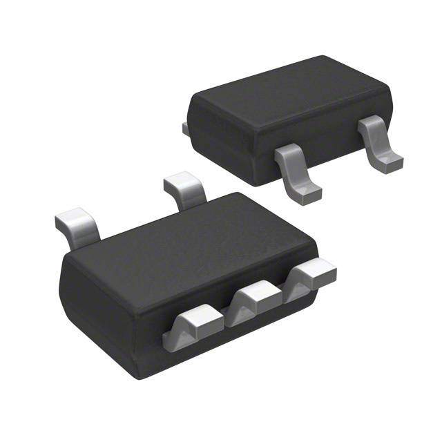
| 产品图片 |
|
| rohs | 符合RoHS无铅 / 符合限制有害物质指令(RoHS)规范要求 |
| 产品系列 | 电源管理 IC,参考电压,Diodes Incorporated ZXRE160H5TA- |
| 数据手册 | |
| 产品型号 | ZXRE160H5TA |
| RoHS指令信息 | http://diodes.com/download/4349 |
| 串联VREF—输入电压—最大值 | 18 V |
| 串联VREF—输入电压—最小值 | 2 V |
| 产品种类 | 参考电压 |
| 供应商器件封装 | SOT-353 |
| 其它名称 | ZXRE160H5TADITR |
| 包装 | 带卷 (TR) |
| 参考类型 | Shunt Adjustable Precision References |
| 商标 | Diodes Incorporated |
| 安装类型 | 表面贴装 |
| 安装风格 | SMD/SMT |
| 容差 | ±1% |
| 封装 | Reel |
| 封装/外壳 | 6-TSSOP(5 引线),SC-88A,SOT-353 |
| 封装/箱体 | SOT-353 |
| 工作温度 | -40°C ~ 125°C |
| 最大工作温度 | + 125 C |
| 最小工作温度 | - 40 C |
| 标准包装 | 3,000 |
| 温度系数 | - |
| 电压-输入 | - |
| 电压-输出 | 0.2 V ~ 18 V |
| 电流-输出 | 15mA |
| 电流-阴极 | 1mA |
| 电流-静态 | - |
| 输出电压 | 0.2 V to 18 V |
| 通道数 | 1 |

.jpg)


- 商务部:美国ITC正式对集成电路等产品启动337调查
- 曝三星4nm工艺存在良率问题 高通将骁龙8 Gen1或转产台积电
- 太阳诱电将投资9.5亿元在常州建新厂生产MLCC 预计2023年完工
- 英特尔发布欧洲新工厂建设计划 深化IDM 2.0 战略
- 台积电先进制程称霸业界 有大客户加持明年业绩稳了
- 达到5530亿美元!SIA预计今年全球半导体销售额将创下新高
- 英特尔拟将自动驾驶子公司Mobileye上市 估值或超500亿美元
- 三星加码芯片和SET,合并消费电子和移动部门,撤换高东真等 CEO
- 三星电子宣布重大人事变动 还合并消费电子和移动部门
- 海关总署:前11个月进口集成电路产品价值2.52万亿元 增长14.8%


PDF Datasheet 数据手册内容提取
A Product Line of Diodes Incorporated ZXRE160 0.6V ENHANCED ADJUSTABLE PRECISION SHUNT REGULATOR Description Pin Assignments ZXRE160_H5 (SC70/SOT353) and The ZXRE160 is a 5-terminal adjustable shunt regulator offering ZXRE160_ET5 (TSOT25) excellent temperature stability and output handling capability. This device offers an enhancement to the ZXRE060 part for use in a TToopp vviieeww comparator mode applications. T In shunt regulator mode, the ZXRE160 simplifies the design of C U isolated low voltage DC-DC regulators. With its low 0.6V FB pin, it can D control the regulation of rails as low 0.6V. This makes the part ideal O for state of the art microprocessor, DSP and PLD core voltage R P POL converters. W The device open-collector output can operate from 0.2V to 18V and ZXRE160_FT4 (X2-DFN1520-6) E regulated output voltage can be set by selection of two external N TToopp vviieeww divider resistors. Separating the input from the open collector output enables the ZXRE160 to be used to make low-cost low drop-out PPGGNNDD 11 66 IINN regulators operating at low input voltages. The ZXRE160 is available in two grades with initial tolerances of 0.5% NN//CC 22 55 GGNNDD and 1% for the A and standard grades respectively. It is available in space saving low profile 5 pin SC70/SOT353, thin TSOT25 and very OOUUTT 33 44 FFBB small DFN1520 packages. EExxppoosseedd ffllaa gg ffllooaattiinngg oorr Features ccoonnnneecctt ttoo GGNNDD • Low reference voltage (VFB = 0.6V) • -40°C to +125°C temperature range Applications • Reference voltage tolerance at +25°C • 0.5% ZXRE160A • Isolated DC-DC converters • 1% ZXRE160 • Core voltage POL • Typical temperature drift • Low Voltage Low-Dropout linear regulators • <4 mV (0°C to +70°C) • Shunt regulators • <6 mV (-40°C to +85°C) • Adjustable voltage reference • <12mV (-40°C to +125°C) • 0.2V to 18V open-collector output • High power supply rejection • (>45dB at 300kHz) • Totally Lead-Free & Fully RoHS Compliant (Notes 1 & 2) • Halogen and Antimony Free. “Green” Device (Note 3) Notes: 1. No purposely added lead. Fully EU Directive 2002/95/EC (RoHS) & 2011/65/EU (RoHS 2) compliant. 2. See http://www.diodes.com for more information about Diodes Incorporated’s definitions of Halogen- and Antimony-free, "Green" and Lead-free. 3. Halogen- and Antimony-free "Green” products are defined as those which contain <900ppm bromine, <900ppm chlorine (<1500ppm total Br + Cl) and <1000ppm antimony compounds. ZXRE160 1 of 15 June 2012 Document number: DS35688 Rev. 2 - 2 www.diodes.com © Diodes Incorporated
A Product Line of Diodes Incorporated ZXRE160 Typical Applications Circuit T C U D O R P W E N Pin Descriptions Package Name Pin Number Pin Name Function SC70/ SOT353, X2-DFN1520-6 TSOT25 Power Ground: Ground return for emitter of output transistor: Connect PGND and PGND 1 1 GND together. — — 2 No connection Output: Connect a capacitor close to device between OUT and GND for closed loop OUT 5 3 stability. See the Applications Information section. FB 4 4 Feedback Input. Threshold voltage 600mV nominal. Analog Ground: Ground return for reference and amplifier: Connect GND and PGND GND 2 5 together. IN 3 6 Supply Input: Connect a 0.1μF ceramic capacitor close to the device from IN to GND. — — Flag Floating or connect to GND ZXRE160 2 of 15 June 2012 Document number: DS35688 Rev. 2 - 2 www.diodes.com © Diodes Incorporated
A Product Line of Diodes Incorporated ZXRE160 Functional Block Diagram T C U D O R P W E N The ZXRE160 differs from most other shunt regulators in that it auxiliary rail voltage, or below the minimum VIN voltage. This has separate input and output pins and a low voltage reference. allows it to operate as a low-dropout voltage regulator for This enables it to regulate rails down to 600mV and makes the microprocessor/DSP/PLD cores. part ideal for isolated power supply applications that use As with other shunt regulators (and shunt references), the opto-couplers in the feedback loop and where the open-collector ZXRE160 compares its internal amplifier FB pin to a high output is required to operate down to voltages as low as 200mV. accuracy internal reference; if FB is below the reference then OUT The wide input voltage range of 2V to 18V and output voltage turns off, but if FB is above the reference then OUT sinks current range of 0.2V to 18V enables the ZXRE160 to be powered from – up to a maximum of 15mA. an auxiliary rail, while controlling a master rail which is above the ZXRE160 3 of 15 June 2012 Document number: DS35688 Rev. 2 - 2 www.diodes.com © Diodes Incorporated
A Product Line of Diodes Incorporated ZXRE160 Absolute Maximum Ratings (Voltages to GND, @TA = +25°C, unless otherwise specified.) Symbol Parameter Rating Unit VIN IN Voltage relative to GND 20 V VOUT OUT Voltage relative to GND 20 V VFB FB Voltage relative to GND 20 V T C PGND PGND Voltage relative to GND -0.3 to +0.3 V U IOUT OUT Pin Current 20 mA D TJ Operating Junction Temperature -40 to 150 °C O TST Storage Temperature 55 to 150 °C R P These are stress ratings only. Operation outside the absolute maximum ratings may cause device failure. Operation at the absolute maximum rating for extended periods may reduce device reliability. W Semiconductor devices are ESD sensitive and may be damaged by exposure to ESD events. E Suitable ESD precautions should be taken when handling and transporting these devices. N Package Thermal Data P DIS Package θ JA T = 25°C, T = 150°C A J SC70/SOT353 400°C/W 310mW TSOT25 250°C/W 500mW X2-DFN1520-6 TBD TBD Recommended Operating Conditions (@TA = +25°C, unless otherwise specified.) Symbol Parameter Min Max Units VIN IN Voltage Range (0 to +125°C) 2 18 VIN IN Voltage Range (-40°C to 0°C) 2.2 18 V VOUT OUT Voltage Range 0.2 18 IOUT OUT Pin Current 0.3 15 mA Operating Ambient Temperature TA -40 +125 °C Range ZXRE160 4 of 15 June 2012 Document number: DS35688 Rev. 2 - 2 www.diodes.com © Diodes Incorporated
A Product Line of Diodes Incorporated ZXRE160 Electrical Characteristics (@TA = +25°C, VDD = 3V, unless otherwise specified.) TA = +25°C, VIN = 3.3V, VOUT = VFB, IOUT = 5mA, unless otherwise specified.) (Note 4) Symbol Parameter Conditions Min Typ Max Units ZXRE160A 0.597 0.6 0.603 ZXRE160 0.594 0.6 0.606 T C ZXRE160A 0.595 0.605 U TA = 0°C to +85°C ZXRE160 0.592 0.608 D O VFB Feedback voltage ZXRE160A 0.594 0.606 V R TA = -40°C to +85°C ZXRE160 0.591 0.609 P W ZXRE160A 0.593 0.607 E TA = -40°C to +125°C N ZXRE160 0.590 0.610 Feedback pin load 3.8 6 FBLOAD IOUT = 1 to 15mA mV regulation TA = -40 to +125°C 10 Feedback pin line VIN = 2V to 18V 0.3 1 FBLINE mV regulation VIN = 2.2V to 18V TA = -40 to +125°C 1.5 VOUT = 0.2V to 18V, 1 Output voltage FBOVR IOUT = 1mA mV regulation TA = -40 to +125°C 1.5 (Ref. Figure 1) -45 IFB FB input bias current VIN = 18V TA = -40 to +125°C -200 0 nA VFB = 0.7V -50 50 VIN = 2V to 18V 0.35 0.7 IOUT = 0.3mA mA VIN = 2.2V to 18V TA = -40 to +125°C 1 IIN Input current VIN = 2V to 18V 0.48 1 IOUT = 10mA VIN = 2.2V to 18V TA = -40 to +125°C 1.5 mA VIN = 18V, IOUT = 0.3mA VFB = 0.7V 3 VIN = 18V, 0.1 IOUT(LK) OUT leakage current VOUT = 18V, µA TA = +125°C 1 VFB =0V Dynamic Output IOUT = 1 to 15mA 0.25 0.4 ZOUT Ω Impedance f < 1kHz TA = -40 to +125°C 0.6 Power supply rejection F = 300kHz PSRR >45 dB ratio VAC = 0.3VPP Amplifier Unity Gain BW Ref: Figure 2 600 kHz Frequency Amplifier G 5000 mA/V Transconductance Note: 4. Production testing of the device is performed at +25°C. Functional operation of the device and parameters specified over the operating temperature range are guaranteed by design, characterization and process control. ZXRE160 5 of 15 June 2012 Document number: DS35688 Rev. 2 - 2 www.diodes.com © Diodes Incorporated
A Product Line of Diodes Incorporated ZXRE160 Typical Characteristics T C U D O R P W E N ZXRE160 6 of 15 June 2012 Document number: DS35688 Rev. 2 - 2 www.diodes.com © Diodes Incorporated
A Product Line of Diodes Incorporated ZXRE160 Typical Operating Characteristics 220000 222255 220000 222255 CCVVOOUUTT==== 0022....6622VVuuFF CCVVOOUUTT==== 0066VV..2222uuFF OOUUTT OOUUTT 115500 118800 115500 118800 T C ODU Gain (dB)Gain (dB)1155000000 9191030355Phase (deg)Phase (deg) Gain (dB)Gain (dB)1100550000 9191030355 Phase (deg)Phase (deg) R P W 00 4455 00 4455 GGGaaaiiinnn GGGaaaiiinnn E PPPhhhaaassseee PPPhhhaaassseee N --5500 00 --5500 00 11 1100 110000 11kk 1100kk 110000kk 11MM 11 1100 110000 11kk 1100kk 110000kk 11MM FFrreeqquueenncc yy ((HHzz)) FFrreeqquu eennccyy ((HHzz)) GGaaiinn aanndd PPhhaassee vvss FFrreeqquueennccyy,, VV ==00..66VV OOUUTT GGaaiinn aanndd PPhhaassee vvssFFrreeqquueennccyy,, VV ==66VV OOUUTT Figure 2. Test Circuits for Gain and Phase Plots ZXRE160 7 of 15 June 2012 Document number: DS35688 Rev. 2 - 2 www.diodes.com © Diodes Incorporated
A Product Line of Diodes Incorporated ZXRE160 Application Information The following show some typical application examples for the ZXRE160. Figure 3 shows a typical configuration for the ZXRE160 in comparator mode. Here the comparator switches low when: T C V (R +R ) U VM ≥ FB 1 2 R D 2 O Alternative values of R1, R2 may be used to provide different threshold R voltages. R3 can also be adjusted to set the bias current for different P values of VM. R2 should be kept as low as possible to minimize errors W due to the bias current of the FB pin. E N This circuit has no hysteresis, so a small capacitor of approx.4.7nF between FB and GND is recommended to provide cleaner transitions at the output. Figure 3. 15V Supply Monitor In shunt regulator mode it is necessary to include the compensation capacitor C2 to guarantee stability. C2 may range in value from 0.1µF to 10µF depending on the application. The minimum value of C2 can be determined from the following equation (resistor values are in kΩ): R C2 ≥ 2 μF MIN R (R +R ) 3 1 2 Both C1 and C2 should be as close to the ZXRE160 as possible and connected to it with the shortest possible track. In the case of Figure 10 and Figure 11, it means the opto-coupler will have to be carefully positioned to enable this. ⎛ R1⎞ VOUT =VREF VOUT=VREF⎜⎝1+R2⎟⎠ R3= VIN−VOUT R3= VIN−VOUT I R3 IR3 Figure 4. 0.6V Shunt Regulator Figure 5. 1.0V Shunt Regulator ZXRE160 8 of 15 June 2012 Document number: DS35688 Rev. 2 - 2 www.diodes.com © Diodes Incorporated
A Product Line of Diodes Incorporated ZXRE160 Application Information (cont.) T C U D O R P W E N VOUT = VREF VOUT=VREF⎜⎝⎛1+RR21⎟⎠⎞ Figure 6. 0.6V Series LDO Regulator Figure 7. 1.0V Series LDO Regulator Design guide: 1. Determine IOUT and choose a suitable transistor taking power dissipation into consideration. I OUT(max) 2. Determine IB from IB = (h +1) FE(min) 3. Determine IR3 from IR3≥IB+IKA(min). The design of the ZXRE160 effectively means there is no IKA(min) limitation as in conventional references. There is only an output leakage current which is a maximum of 1µA. Nevertheless, it is necessary to determine an IKA(min) to ensure that the device operates within its linear range at all times. IKA(min) ≥ 10µA should be adequate for this. V −(V +V ) 4. Determine R3 from R3= IN OUT BE . I R3 Although unlikely to be a problem, ensure that IR3 ≤ 15 mA. ZXRE160 9 of 15 June 2012 Document number: DS35688 Rev. 2 - 2 www.diodes.com © Diodes Incorporated
A Product Line of Diodes Incorporated ZXRE160 Application Information (cont.) ⎛ R1⎞ V =V ⎜1+ ⎟ OUT REF ⎝ R2⎠ T V ≥0.2V+V C OUT BE U D O R3= VIN−VOUT I R R3 P W Figure 8. 1V Current-Boosted Shunt Regulator E N Design guide 1. Determine IOUT and choose a suitable transistor taking power dissipation into consideration. I 2. Determine IB from I = OUT(max) B (h +1) FE(min) 3. Determine IR3 from IR3 =IOUT(max) V −V 4. Determine R3 from R3= IN OUT I R3 5. It is best to let the ZXRE160 supply as much current as it can before bringing Q1 into conduction. Not only does this minimize the strain on Q1, it also guarantees the most stable operation. Choose a nominal value between 10mA and <15mA for this current, IR4. V Calculate R4 from R4= BE I R4 VOUT goes low and LED is lit when monitored supply ⎛ R1⎞ VM>VREF⎜1+ ⎟ ⎝ R2⎠ VIN−(VF+0.2) R3= IR3 15mA≥IR3≤IF(MAX) VF and IF are forward voltage drop and current of LED1. Figure 9. 1.15V Over-Voltage Indicator ZXRE160 10 of 15 June 2012 Document number: DS35688 Rev. 2 - 2 www.diodes.com © Diodes Incorporated
A Product Line of Diodes Incorporated ZXRE160 Application Information (cont.) T C U D O R P W ⎛ R1⎞ E VOUT =VREF VOUT =VREF⎜⎝1+R2⎟⎠ N V −(V +0.2) R3= IN I F R3= VIN−(VF+0.2) R3 I R3 15mA≥I ≤I R3 F(MAX) 15mA≥IR3 ≤IF(MAX) Figure 10. Opto-Isolated 0.6V Shunt Regulator Figure 11. Opto-Isolated 1.0V Shunt Regulator VF and IF are forward voltage drop and forward current respectively for the optocoupler LED More applications information is available in the following publications which can be found on Diodes’ web site. AN58 - Designing with Diodes’ References – Shunt Regulation AN59 - Designing with Diodes’ References – Series Regulation AN60 - Designing with Diodes’ References – Fixed Regulators and Opto-Isolation AN61 - Designing with Diodes’ References – Extending the operating voltage range AN62 - Designing with Diodes’ References – Other Applications AN63 - Designing with Diodes’ References – ZXRE060 Low Voltage Regulator ZXRE160 11 of 15 June 2012 Document number: DS35688 Rev. 2 - 2 www.diodes.com © Diodes Incorporated
A Product Line of Diodes Incorporated ZXRE160 Ordering Information T C U D O R P W Identification E Tol. Part Number Package Reel Size Tape Width Quantity/Reel Code N ZXRE160AET5TA TSOT25 R8 7”, 180mm 8mm 3000 0.5% ZXRE160AH5TA SC70/SOT353 R9 7”, 180mm 8mm 3000 ZXRE160AFT4-7 DFN1520H4-6 R8 7”, 180mm 8mm 3000 ZXRE160ET5TA TSOT25 Z8 7”, 180mm 8mm 3000 1% ZXRE160H5TA SC70/SOT353 Z9 7”, 180mm 8mm 3000 ZXRE160FT4-7 X2-DFN1520-6 Z8 7”, 180mm 8mm 3000 Marking Information 1. TSOT25, SC70/SOT353 2. X2-DFN1520-6 ZXRE160 12 of 15 June 2012 Document number: DS35688 Rev. 2 - 2 www.diodes.com © Diodes Incorporated
A Product Line of Diodes Incorporated ZXRE160 Package Outline Dimensions (All dimensions in mm.) TSOT25 TSOT25 D Dim Min Max Typ e1 A − 1.00 − A1 0.01 0.10 − T A2 0.84 0.90 − C D − − 2.90 U E1 E E − − 2.80 D E1 − − 1.60 O c L2 b 0.30 0.45 − R θ c 0.12 0.20 − L P e 4x θ1 e − − 0.95 e1 − − 1.90 W 5x b L 0.30 0.50 E L2 − − 0.25 N A A2 θ 0° 8° 4° θ1 4° 12° − A1 All Dimensions in mm SC70/SOT353 A SOT353 Dim Min Max A 0.10 0.30 B C B 1.15 1.35 C 2.00 2.20 D 0.65 Typ F 0.40 0.45 H 1.80 2.20 H J 0 0.10 K 0.90 1.00 K M L 0.25 0.40 M 0.10 0.22 J α 0° 8° D F L All Dimensions in mm X2-DFN1520-6 A3 A SEATING PLANE X2-DFN1520-6 A1 Dim Min Max Typ D A − 0.40 − e A1 0 0.05 − A3 − − 0.13 L b 0.20 0.30 − D 1.45 1.575 − D2 1.00 1.20 − e − − 0.50 E E2 E 1.95 2.075 − D2 E2 0.70 0.90 − L 0.25 0.35 − All Dimensions in mm b ZXRE160 13 of 15 June 2012 Document number: DS35688 Rev. 2 - 2 www.diodes.com © Diodes Incorporated
A Product Line of Diodes Incorporated ZXRE160 Suggested Pad Layout TSOT25 C C Dimensions Value (in mm) C 0.950 T C X 0.700 U Y1 Y 1.000 Y1 3.199 D O R Y (5x) P W X (5x) E SC70/SOT353 N C2 C2 Dimensions Value (in mm) Z 2.5 G 1.3 X 0.42 G C1 Z Y 0.6 C1 1.9 C2 0.65 Y X X2-DFN1520-6 C1 C G2 G1 Dimensions Value (in mm) Z 1.25 G1 0.45 X1 G2 0.15 X1 1.10 C 0.50 C1 0.25 G2 Z ZXRE160 14 of 15 June 2012 Document number: DS35688 Rev. 2 - 2 www.diodes.com © Diodes Incorporated
A Product Line of Diodes Incorporated ZXRE160 IMPORTANT NOTICE DIODES INCORPORATED MAKES NO WARRANTY OF ANY KIND, EXPRESS OR IMPLIED, WITH REGARDS TO THIS DOCUMENT, INCLUDING, BUT NOT LIMITED TO, THE IMPLIED WARRANTIES OF MERCHANTABILITY AND FITNESS FOR A PARTICULAR PURPOSE (AND THEIR EQUIVALENTS UNDER THE LAWS OF ANY JURISDICTION). Diodes Incorporated and its subsidiaries reserve the right to make modifications, enhancements, improvements, corrections or other changes T without further notice to this document and any product described herein. Diodes Incorporated does not assume any liability arising out of the C application or use of this document or any product described herein; neither does Diodes Incorporated convey any license under its patent or U trademark rights, nor the rights of others. Any Customer or user of this document or products described herein in such applications shall assume all risks of such use and will agree to hold Diodes Incorporated and all the companies whose products are represented on Diodes Incorporated D website, harmless against all damages. O R Diodes Incorporated does not warrant or accept any liability whatsoever in respect of any products purchased through unauthorized sales channel. P Should Customers purchase or use Diodes Incorporated products for any unintended or unauthorized application, Customers shall indemnify and hold Diodes Incorporated and its representatives harmless against all claims, damages, expenses, and attorney fees arising out of, directly or W indirectly, any claim of personal injury or death associated with such unintended or unauthorized application. E N Products described herein may be covered by one or more United States, international or foreign patents pending. Product names and markings noted herein may also be covered by one or more United States, international or foreign trademarks. LIFE SUPPORT Diodes Incorporated products are specifically not authorized for use as critical components in life support devices or systems without the express written approval of the Chief Executive Officer of Diodes Incorporated. As used herein: A. Life support devices or systems are devices or systems which: 1. are intended to implant into the body, or 2. support or sustain life and whose failure to perform when properly used in accordance with instructions for use provided in the labeling can be reasonably expected to result in significant injury to the user. B. A critical component is any component in a life support device or system whose failure to perform can be reasonably expected to cause the failure of the life support device or to affect its safety or effectiveness. Customers represent that they have all necessary expertise in the safety and regulatory ramifications of their life support devices or systems, and acknowledge and agree that they are solely responsible for all legal, regulatory and safety-related requirements concerning their products and any use of Diodes Incorporated products in such safety-critical, life support devices or systems, notwithstanding any devices- or systems-related information or support that may be provided by Diodes Incorporated. Further, Customers must fully indemnify Diodes Incorporated and its representatives against any damages arising out of the use of Diodes Incorporated products in such safety-critical, life support devices or systems. Copyright © 2012, Diodes Incorporated www.diodes.com ZXRE160 15 of 15 June 2012 Document number: DS35688 Rev. 2 - 2 www.diodes.com © Diodes Incorporated
Mouser Electronics Authorized Distributor Click to View Pricing, Inventory, Delivery & Lifecycle Information: D iodes Incorporated: ZXRE160FT4-7 ZXRE160AFT4-7 ZXRE160AET5TA ZXRE160H5TA ZXRE160ET5TA ZXRE160AH5TA