ICGOO在线商城 > 集成电路(IC) > PMIC - 电压基准 > REF2925AIDBZR
 Datasheet下载
- 型号: REF2925AIDBZR
- 制造商: Texas Instruments
- 库位|库存: xxxx|xxxx
- 要求:
| 数量阶梯 | 香港交货 | 国内含税 |
| +xxxx | $xxxx | ¥xxxx |
查看当月历史价格
查看今年历史价格
REF2925AIDBZR产品简介:
ICGOO电子元器件商城为您提供REF2925AIDBZR由Texas Instruments设计生产,在icgoo商城现货销售,并且可以通过原厂、代理商等渠道进行代购。 REF2925AIDBZR价格参考。Texas InstrumentsREF2925AIDBZR封装/规格:PMIC - 电压基准, 系列 电压基准 IC ±2% 25mA SOT-23-3。您可以下载REF2925AIDBZR参考资料、Datasheet数据手册功能说明书,资料中有REF2925AIDBZR 详细功能的应用电路图电压和使用方法及教程。
Texas Instruments(德州仪器)的REF2925AIDBZR是一款PMIC(电源管理集成电路)中的电压基准芯片,广泛应用于需要高精度、低噪声和稳定电压基准的场景。以下是其主要应用场景:

1. 精密测量与测试设备:在要求高精度电压基准的测试和测量设备中,如数字万用表、示波器等,REF2925AIDBZR可以提供稳定的参考电压,确保测量结果的准确性。

2. 数据采集系统:用于工业自动化、医疗设备和环境监测等领域中的数据采集系统,REF2925AIDBZR能够为模数转换器(ADC)和数模转换器(DAC)提供精确的参考电压,从而提高系统的测量精度和稳定性。

3. 传感器接口电路:在各种传感器应用中,如温度、压力、湿度传感器等,REF2925AIDBZR可以为传感器信号调理电路提供稳定的参考电压,确保传感器输出信号的准确性和可靠性。

4. 通信设备:在无线通信基站、路由器等通信设备中,REF2925AIDBZR可用于提供稳定的电源基准,确保通信信号的稳定传输和接收,减少干扰和误码率。

5. 电源管理系统:在便携式电子设备、电池管理系统(BMS)等应用中,REF2925AIDBZR可以为电源监控和管理电路提供精确的电压基准,帮助实现高效的电源管理和保护功能。

6. 汽车电子:在汽车电子系统中,如发动机控制单元(ECU)、车身控制系统等,REF2925AIDBZR可以为这些系统提供可靠的电压基准,确保车辆各部件的正常运行和安全性。

总之,REF2925AIDBZR凭借其高精度、低噪声和稳定性,在各种需要精确电压基准的应用场景中表现出色,广泛应用于工业、医疗、通信、消费电子和汽车电子等领域。
| 参数 | 数值 |
| 产品目录 | 集成电路 (IC)半导体 |
| 描述 | IC VREF SERIES PREC 2.5V SOT23-3参考电压 2.5V 100ppm/DegC 50uA SOT23-3 Series |
| 产品分类 | |
| 品牌 | Texas Instruments |
| 产品手册 | |
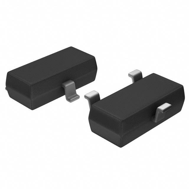
| 产品图片 |
|
| rohs | 符合RoHS无铅 / 符合限制有害物质指令(RoHS)规范要求 |
| 产品系列 | 电源管理 IC,参考电压,Texas Instruments REF2925AIDBZR- |
| 数据手册 | |
| 产品型号 | REF2925AIDBZR |
| 串联VREF—电源电流—最大值 | 50 uA |
| 串联VREF—输入电压—最大值 | 5.5 V |
| 串联VREF—输入电压—最小值 | 2.501 V |
| 产品种类 | 参考电压 |
| 供应商器件封装 | SOT-23-3 |
| 其它名称 | 296-32211-6 |
| 分流电流—最大值 | 25 mA |
| 初始准确度 | 2 % |
| 包装 | Digi-Reel® |
| 参考类型 | Series References |
| 商标 | Texas Instruments |
| 安装类型 | 表面贴装 |
| 安装风格 | SMD/SMT |
| 容差 | ±2% |
| 封装 | Reel |
| 封装/外壳 | TO-236-3,SC-59,SOT-23-3 |
| 封装/箱体 | SOT-23-3 |
| 工作温度 | -40°C ~ 125°C |
| 工厂包装数量 | 3000 |
| 平均温度系数—典型值 | 100 PPM / C |
| 最大工作温度 | + 125 C |
| 最小工作温度 | - 40 C |
| 标准包装 | 1 |
| 温度系数 | 100ppm/°C |
| 电压-输入 | 2.501 V ~ 5.5 V |
| 电压-输出 | 2.5V |
| 电流-输出 | 25mA |
| 电流-阴极 | - |
| 电流-静态 | 50µA |
| 电源电流 | 42 uA |
| 系列 | REF2925 |
| 输出电压 | 2.5 V |
| 通道数 | 1 |


- 商务部:美国ITC正式对集成电路等产品启动337调查
- 曝三星4nm工艺存在良率问题 高通将骁龙8 Gen1或转产台积电
- 太阳诱电将投资9.5亿元在常州建新厂生产MLCC 预计2023年完工
- 英特尔发布欧洲新工厂建设计划 深化IDM 2.0 战略
- 台积电先进制程称霸业界 有大客户加持明年业绩稳了
- 达到5530亿美元!SIA预计今年全球半导体销售额将创下新高
- 英特尔拟将自动驾驶子公司Mobileye上市 估值或超500亿美元
- 三星加码芯片和SET,合并消费电子和移动部门,撤换高东真等 CEO
- 三星电子宣布重大人事变动 还合并消费电子和移动部门
- 海关总署:前11个月进口集成电路产品价值2.52万亿元 增长14.8%


PDF Datasheet 数据手册内容提取
Product Sample & Technical Tools & Support & Reference Folder Buy Documents Software Community Design REF2912,REF2920,REF2925 REF2930,REF2933,REF2940 SBVS033C–JUNE2002–REVISEDJUNE2016 REF29xx 100 ppm/°C, 50 µA in 3-Pin SOT-23 CMOS Voltage Reference 1 Features 3 Description • MicroSIZEPackage:SOT-23 The REF29xx is a precision, low-power, low-voltage 1 dropout voltage reference family available in a tiny • LowDropout:1mV 3‑pinSOT-23package. • HighOutputCurrent:25mA The small size and low power consumption (50 µA • LowTemperatureDrift:Maximumof100ppm/°C maximum) of the REF29xx make it ideal for portable • HighAccuracy:2% andbattery-poweredapplications.TheREF29xxdoes • LowI :Maximumof50µA not require a load capacitor, but it is stable with any Q capacitiveload. 2 Applications Unloaded, the REF29xx can be operated with supplies within 1 mV of output voltage. All models are • Portable,Battery-PoweredEquipment specified for the wide temperature range, –40°C to • DataAcquisitionSystems 125°C. • MedicalEquipment • Hand-HeldTestEquipment DeviceInformation(1) PARTNUMBER PACKAGE BODYSIZE(NOM) REF29xx SOT-23(3) 2.92mm×1.30mm (1) For all available packages, see the orderable addendum at theendofthedatasheet. DropoutVoltagevsLoadCurrent 350 300 V) 250 m e ( ag 200 olt V ut 150 o p Dro 100 50 0 0 5 10 15 20 25 30 Load Current (mA) 1 An IMPORTANT NOTICE at the end of this data sheet addresses availability, warranty, changes, use in safety-critical applications, intellectualpropertymattersandotherimportantdisclaimers.PRODUCTIONDATA.
REF2912,REF2920,REF2925 REF2930,REF2933,REF2940 SBVS033C–JUNE2002–REVISEDJUNE2016 www.ti.com Table of Contents 1 Features.................................................................. 1 8.4 DeviceFunctionalModes........................................13 2 Applications........................................................... 1 9 ApplicationandImplementation........................ 15 3 Description............................................................. 1 9.1 ApplicationInformation............................................15 4 RevisionHistory..................................................... 2 9.2 TypicalApplication..................................................15 5 DeviceComparisonTable..................................... 3 10 PowerSupplyRecommendations..................... 18 6 PinConfigurationandFunctions......................... 3 11 Layout................................................................... 18 11.1 LayoutGuidelines.................................................18 7 Specifications......................................................... 4 11.2 LayoutExample....................................................18 7.1 AbsoluteMaximumRatings......................................4 12 DeviceandDocumentationSupport................. 19 7.2 ESDRatings..............................................................4 7.3 RecommendedOperatingConditions.......................4 12.1 RelatedLinks........................................................19 7.4 ThermalInformation..................................................4 12.2 ReceivingNotificationofDocumentationUpdates19 7.5 ElectricalCharacteristics...........................................5 12.3 CommunityResources..........................................19 7.6 TypicalCharacteristics..............................................7 12.4 Trademarks...........................................................19 12.5 ElectrostaticDischargeCaution............................19 8 DetailedDescription............................................ 11 12.6 Glossary................................................................19 8.1 Overview.................................................................11 13 Mechanical,Packaging,andOrderable 8.2 FunctionalBlockDiagram.......................................11 Information........................................................... 19 8.3 FeatureDescription.................................................11 4 Revision History ChangesfromRevisionB(February2008)toRevisionC Page • AddedESDRatingstable,ThermalInformationtable,FeatureDescriptionsection,DeviceFunctionalModes, ApplicationandImplementationsection,PowerSupplyRecommendationssection,Layoutsection,Deviceand DocumentationSupportsection,andMechanical,Packaging,andOrderableInformationsection....................................... 1 • DeletedOrderingInformationtable;seePOAattheendofthedatasheet........................................................................... 1 2 SubmitDocumentationFeedback Copyright©2002–2016,TexasInstrumentsIncorporated ProductFolderLinks:REF2912 REF2920 REF2925REF2930 REF2933 REF2940
REF2912,REF2920,REF2925 REF2930,REF2933,REF2940 www.ti.com SBVS033C–JUNE2002–REVISEDJUNE2016 5 Device Comparison Table PRODUCT VOLTAGE(V) REF2912 1.25 REF2920 2.048 REF2925 2.5 REF2930 3 REF2933 3.3 REF2940 4.096 6 Pin Configuration and Functions DBZPackage 3-PinSOT-23 TopView IN 1 REF2912 REF2920 REF2925 3 GND REF2930 REF2933 OUT 2 REF2940 PinFunctions PIN I/O DESCRIPTION NO. NAME 1 IN I Inputsupplyvoltage 2 OUT O Referenceoutputvoltage 3 GND — Ground Copyright©2002–2016,TexasInstrumentsIncorporated SubmitDocumentationFeedback 3 ProductFolderLinks:REF2912 REF2920 REF2925REF2930 REF2933 REF2940
REF2912,REF2920,REF2925 REF2930,REF2933,REF2940 SBVS033C–JUNE2002–REVISEDJUNE2016 www.ti.com 7 Specifications 7.1 Absolute Maximum Ratings overoperatingfree-airtemperaturerange(unlessotherwisenoted)(1) MIN MAX UNIT Supplyvoltage,V+toV– 7 V Outputshortcircuit(2) Continuous °C Leadtemperature(soldering,10s) 300 °C Operatingtemperature –40 125 °C Junctiontemperature 150 °C Storagetemperature,T –65 150 °C stg (1) StressesbeyondthoselistedunderAbsoluteMaximumRatingsmaycausepermanentdamagetothedevice.Thesearestressratings only,whichdonotimplyfunctionaloperationofthedeviceattheseoranyotherconditionsbeyondthoseindicatedunderRecommended OperatingConditions.Exposuretoabsolute-maximum-ratedconditionsforextendedperiodsmayaffectdevicereliability. (2) Short-circuittoground. 7.2 ESD Ratings VALUE UNIT Human-bodymodel(HBM),perANSI/ESDA/JEDECJS-001(1) ±4000 V Electrostaticdischarge V (ESD) Charged-devicemodel(CDM),perJEDECspecificationJESD22-C101(2) ±1500 (1) JEDECdocumentJEP155statesthat500-VHBMallowssafemanufacturingwithastandardESDcontrolprocess. (2) JEDECdocumentJEP157statesthat250-VCDMallowssafemanufacturingwithastandardESDcontrolprocess. 7.3 Recommended Operating Conditions overoperatingfree-airtemperaturerange(unlessotherwisenoted) MIN MAX UNIT V Inputvoltage V +0.05(1) 5.5 V IN REF I Loadcurrent 25 mA LOAD T Operatingtemperature –40 125 °C A (1) MinimumsupplyvoltagefortheREF2912is1.8V. 7.4 Thermal Information REF29xx THERMALMETRIC(1) DBZ(SOT-23) UNIT 3PINS R Junction-to-ambientthermalresistance 297.3 °C/W θJA R Junction-to-case(top)thermalresistance 128.5 °C/W θJC(top) R Junction-to-boardthermalresistance 91.7 °C/W θJB ψ Junction-to-topcharacterizationparameter 12.8 °C/W JT ψ Junction-to-boardcharacterizationparameter 90.3 °C/W JB R Junction-to-case(bottom)thermalresistance N/A °C/W θJC(bot) (1) Formoreinformationabouttraditionalandnewthermalmetrics,seetheSemiconductorandICPackageThermalMetricsapplication report. 4 SubmitDocumentationFeedback Copyright©2002–2016,TexasInstrumentsIncorporated ProductFolderLinks:REF2912 REF2920 REF2925REF2930 REF2933 REF2940
REF2912,REF2920,REF2925 REF2930,REF2933,REF2940 www.ti.com SBVS033C–JUNE2002–REVISEDJUNE2016 7.5 Electrical Characteristics Boldfacelimitsapplyoverthespecifiedtemperaturerange,T =–40°Cto125°C.AtT =25°C,I =0mA,V =5V, A A LOAD IN unlessotherwisenoted. PARAMETER TESTCONDITIONS MIN TYP MAX UNIT REF2912–1.25V V Outputvoltage 1.225 1.25 1.275 V OUT Initialaccuracy 2% Outputvoltagenoise f=0.1Hzto10Hz, 14 µV PP Voltagenoise f=10Hzto10kHz 42 µVrms Lineregulation 1.8V≤V ≤5.5V 60 190 µV/V IN REF2920 V Outputvoltage 2.007 2.048 2.089 V OUT Initialaccuracy 2% Outputvoltagenoise f=0.1Hzto10Hz, 23 µV PP Voltagenoise f=10Hzto10kHz 65 µVrms Lineregulation V +50mV≤V ≤5.5V 110 290 µV/V REF IN REF2925 V Outputvoltage 2.45 2.5 2.55 V OUT Initialaccuracy 2% Outputvoltagenoise f=0.1Hzto10Hz 28 µV PP Voltagenoise f=10Hzto10kHz 80 µVrms Lineregulation V +50mV≤V ≤5.5V 120 325 µV/V REF IN REF2930 V Outputvoltage 2.94 3 3.06 V OUT Initialaccuracy 2% Outputvoltagenoise f=0.1Hzto10Hz, 33 µV PP Voltagenoise f=10Hzto10kHz 94 µVrms Lineregulation V +50mV≤V ≤5.5V 120 375 µV/V REF IN REF2933 V Outputvoltage 3.234 3.3 3.366 V OUT Initialaccuracy 2% Outputvoltagenoise f=0.1Hzto10Hz, 36 µV PP Voltagenoise f=10Hzto10kHz 105 µVrms Lineregulation V +50mV≤V ≤5.5V 130 400 µV/V REF IN REF2940 V Outputvoltage 4.014 4.096 4.178 V OUT Initialaccuracy 2% Outputvoltagenoise f=0.1Hzto10Hz, 45 µV PP Voltagenoise f=10Hzto10kHz 128 µVrms V +50mV≤V ≤5.5V 160 410 µV/V REF IN REF2912,REF2920,REF2925,REF2930,REF2933,REF2940 dV /dT Outputvoltagetemperaturedrift(1) –40°C≤T ≤125°C 35 100 ppm/°C OUT A I Outputcurrent 25 mA LOAD 0to1000 24 H Long-termstability ppm 1000to2000 15 H dVOUT/dILOAD Loadregulation(2) 0VmA=V<ILOA+D5<0205mmVA(3,) 3 100 µV/mA IN REF (1) BoxMethodusedtodetermineovertemperaturedrift. (2) Typicalvalueofloadregulationreflectsmeasurementsusingaforceandsensecontacts,seeLoadRegulation. (3) MinimumsupplyvoltageforREF2912is1.8V. Copyright©2002–2016,TexasInstrumentsIncorporated SubmitDocumentationFeedback 5 ProductFolderLinks:REF2912 REF2920 REF2925REF2930 REF2933 REF2940
REF2912,REF2920,REF2925 REF2930,REF2933,REF2940 SBVS033C–JUNE2002–REVISEDJUNE2016 www.ti.com Electrical Characteristics (continued) Boldfacelimitsapplyoverthespecifiedtemperaturerange,T =–40°Cto125°C.AtT =25°C,I =0mA,V =5V, A A LOAD IN unlessotherwisenoted. PARAMETER TESTCONDITIONS MIN TYP MAX UNIT dT ThermalHysteresis(4) 25 100 ppm V –V Dropoutvoltage 1 50 mV IN OUT I Short-circuitcurrent 45 mA SC Turnonsettlingtime to0.1%atV =5VwithC =0 120 µs IN L POWERSUPPLY Voltage I =0 V +0.001(5) 5.5 L REF V V S Voltageovertemperature –40°C≤T ≤125°C V +0.05 5.5 A REF Quiescentcurrent 42 50 I µA Q Quiescentcurrentovertemperature –40°C≤T ≤125°C 59 A TEMPERATURERANGE Specifiedrange –40 125 °C Operatingrange –40 125 °C Storagerange –65 150 °C RθJC ThermalresistanceforSOT-23 110 °C/W R surface-mount 336 °C/W θJA (4) ThermalhysteresisprocedureisexplainedinmoredetailinThermalHysteresis. (5) ForIL>0,seeTypicalCharacteristics. 6 SubmitDocumentationFeedback Copyright©2002–2016,TexasInstrumentsIncorporated ProductFolderLinks:REF2912 REF2920 REF2925REF2930 REF2933 REF2940
REF2912,REF2920,REF2925 REF2930,REF2933,REF2940 www.ti.com SBVS033C–JUNE2002–REVISEDJUNE2016 7.6 Typical Characteristics 50 100 45 90 40 80 s 35 s 70 nit nit U 30 U 60 of of er 25 er 50 b b m 20 m 40 u u N 15 N 30 10 20 5 10 0 0 5 10 15 20 25 30 35 40 45 50 55 60 65 5 10 15 20 25 30 35 40 45 50 55 60 65 Drift (ppm/°C) Drift (ppm/°C) Figure1.TemperatureDrift(0°Cto70°C) Figure2.TemperatureDrift(–40°Cto125°C) 2.502 35 2.500 A) 30 m ge (V) 2.498 urrent ( 25 a C olt 2.496 d 20 V a Output 2.494 mum Lo 15 xi a 2.492 M 10 2.490 5 –40 –20 0 20 40 60 80 100 120 140 –40 –20 0 20 40 60 80 100 120 140 Temperature (°C) Temperature (°C) Figure3.OutputVoltagevsTemperature Figure4.MaximumLoadCurrentvsTemperature 6 60 5 50 A) m V/ 4 40 µ on ( A) ati 3 (µ 30 ul Q g I e R 2 20 d a o L 1 10 0 0 –40 –20 0 20 40 60 80 100 120 140 –40 –20 0 20 40 60 80 100 120 140 Temperature (°C) Temperature (°C) Figure5.LoadRegulationvsTemperature Figure6.QuiescentCurrentvsTemperature Copyright©2002–2016,TexasInstrumentsIncorporated SubmitDocumentationFeedback 7 ProductFolderLinks:REF2912 REF2920 REF2925REF2930 REF2933 REF2940
REF2912,REF2920,REF2925 REF2930,REF2933,REF2940 SBVS033C–JUNE2002–REVISEDJUNE2016 www.ti.com Typical Characteristics (continued) 200 100 150 µV/V) e (dB) 10 ation ( 100 edanc 1 Regul 50 ut Imp Line Outp 0.1 0 –50 0.01 –40 –20 0 20 40 60 80 100 120 140 1 10 100 1k 10k 100k Temperature (°C) Frequency (Hz) Figure7.LineRegulationvsTemperature Figure8.OutputImpedancevsFrequency 90 2.50138 80 2.50000 70 2.49862 dB) 6500 age (V) 22..4499752846 R( olt PSR 40 put V 2.49448 30 ut 2.49310 O 20 2.49172 10 2.49034 0 2.48896 1 10 100 1k 10k 100k 2.5 3 3.5 4 4.5 5 5.5 6 Frequency (Hz) Supply (V) Figure9.Power-SupplyRejectionRatiovsFrequency Figure10.OutputVoltagevsSupplyVoltage(NoLoad) 2.5008 2.50152 2.5000 2.50000 2.4992 2.49848 e (V) 2.4984 e (V) 2.49696 ag 2.4976 ag olt olt 2.49544 put V 2.4968 put V 2.49392 ut 2.4967 ut O O 2.49824 2.4952 2.4944 2.49088 2.4936 2.48936 2.5 3 3.5 4 4.5 5 5.5 6 0 5 10 15 20 25 30 Supply (V) Load Current (mA) Figure11.OutputVoltagevsSupplyVoltage(I =25mA) Figure12.OutputVoltagevsLoadCurrent LOAD 8 SubmitDocumentationFeedback Copyright©2002–2016,TexasInstrumentsIncorporated ProductFolderLinks:REF2912 REF2920 REF2925REF2930 REF2933 REF2940
REF2912,REF2920,REF2925 REF2930,REF2933,REF2940 www.ti.com SBVS033C–JUNE2002–REVISEDJUNE2016 Typical Characteristics (continued) div VIN div VIN V/ V/ 3 5 div VOUT div VOUT V/ V/ 1 1 40µs/div 10µs/div Figure13.StepResponse,C =0,3-VStart-Up Figure14.StepResponse,C =0,5-VStart-Up L L I = 1mA L v di V V/ IN I = 0mA m L 0 0 5 v di V/ V/div VOUT 20m VOUT m 0 5 10µs/div 10µs/div Figure15.LineTransientResponse Figure16.0to1-mALoadTransient(C =0) L IL= 5mA ILL= 0mA IL= 6mA IL= 0mA V/div V/div 20m VOUT 20m VOUT 10µs/div 40µs/div Figure17.0to5-mALoadTransient(CL=0) Figure18.1to6-mALoadTransient(CL=1µF) Copyright©2002–2016,TexasInstrumentsIncorporated SubmitDocumentationFeedback 9 ProductFolderLinks:REF2912 REF2920 REF2925REF2930 REF2933 REF2940
REF2912,REF2920,REF2925 REF2930,REF2933,REF2940 SBVS033C–JUNE2002–REVISEDJUNE2016 www.ti.com Typical Characteristics (continued) I = 25mA L I = 1mA L v v V/di VOUT V/di m µ 20 0 1 100µs/div 1.0s/div Figure19.1to25-mALoadTransient(CL=1µF) Figure20.0.1to10-HzNoise 80 80 Drift (ppm) 7600 Drift (ppm) 7600 Voltage 5400 Voltage 5400 Output 30 Output 30 Absolute 2100 Absolute 2100 0 0 0 100 200 300 400 500 600 700 800 900 1000 1000 1100 1200 1300 1400 1500 1600 1700 1800 1900 2000 Time (hours) Time (hours) Figure21.Long-TermStability0to1000Hours Figure22.Long-TermStability1000to2000Hours 80 m) 70 p p Drift ( 60 ge 50 a Volt 40 ut utp 30 O e 20 ut ol bs 10 A 0 0 200 400 600 800 1000 1200 1400 1600 1800 2000 Time (hours) Figure23.Long-TermStability0to2000Hours 10 SubmitDocumentationFeedback Copyright©2002–2016,TexasInstrumentsIncorporated ProductFolderLinks:REF2912 REF2920 REF2925REF2930 REF2933 REF2940
REF2912,REF2920,REF2925 REF2930,REF2933,REF2940 www.ti.com SBVS033C–JUNE2002–REVISEDJUNE2016 8 Detailed Description 8.1 Overview TheREF29xxisaseries,CMOS,precisionband-gapvoltagereference.ItsbasictopologyisshowninFunctional Block Diagram. The transistors Q and Q are biased such that the current density of Q is greater than that of 1 2 1 Q . The difference of the two base-emitter voltages, Vbe – Vbe , has a positive temperature coefficient and is 2 1 2 forced across resistor R1. This voltage is gained up and added to the base-emitter voltage of Q , which has a 2 negative coefficient. The resulting output voltage is virtually independent of temperature. The curvature of the band-gap voltage, as seen in Figure 3, is due to the slightly nonlinear temperature coefficient of the base-emitter voltageofQ . 2 8.2 Functional Block Diagram R1 + + Vbe Vbe – 1 –2 Q Q 1 2 Copyright © 2016,Texas Instruments Incorporated Figure24. SimplifiedSchematicofBand-GapReference 8.3 Feature Description 8.3.1 SupplyVoltage The REF29xx family of references features an extremely low dropout voltage. With the exception of the REF2912, which has a minimum supply requirement of 1.8 V, the REF29xx can be operated with a supply of only 1 mV above the output voltage in an unloaded condition. For loaded conditions, see Dropout Voltage vs LoadCurrent. The REF29xx features a low quiescent current, which is extremely stable over changes in both temperature and supply. The typical room temperature quiescent current is 42 µA, and the maximum quiescent current over temperature is just 59 µA. Additionally, the quiescent current typically changes less than 2.5 µA over the entire supplyrange,asshowninFigure25. 42.5 42.0 41.5 A) µ ( Q I 41.0 40.5 40.0 1 1.5 2 2.5 3 3.5 4 4.5 5 5.5 6 V (V) IN Figure25. SupplyCurrentvsSupplyVoltage Copyright©2002–2016,TexasInstrumentsIncorporated SubmitDocumentationFeedback 11 ProductFolderLinks:REF2912 REF2920 REF2925REF2930 REF2933 REF2940
REF2912,REF2920,REF2925 REF2930,REF2933,REF2940 SBVS033C–JUNE2002–REVISEDJUNE2016 www.ti.com Feature Description (continued) Supply voltages below the specified levels can cause the REF29xx to momentarily draw currents greater than the typical quiescent current. Using a power supply with a fast rising edge and low output impedance easily preventsthis. 8.3.2 ThermalHysteresis Thermal hysteresis for the REF29xx is defined as the change in output voltage after operating the device at 25°C, cycling the device through the specified temperature range, and returning to 25°C, and can be expressed asshowninEquation1. æabsV -V ö V =ç PRE POST ÷´106(ppm) HYST V è NOM ø where • V =calculatedhysteresis HYST • V =outputvoltagemeasuredat25°Cpretemperaturecycling PRE • V =outputvoltagemeasuredwhendevicehasbeenoperatedat25°C,cycledthroughspecifiedrange POST –40°Cto125°Candreturnedtooperationat25°C (1) 8.3.3 TemperatureDrift The REF29xx is designed to exhibit minimal drift error, defined as the change in output voltage over varying temperature. Using the box method of drift measurement, the REF29xx features a typical drift coefficient of 20 ppm from 0°C to 70°C— the primary temperature range of use for many applications. For industrial temperature rangesof–40°Cto125°C,theREF29xxfamilydriftincreasestoatypicalvalueof50ppm. 8.3.4 NoisePerformance The REF29xx generates noise less than 50 µV between frequencies of 0.1 Hz to 10 Hz, and can be seen in PP Figure20.ThenoisevoltageoftheREF29xxincreaseswithoutputvoltageandoperatingtemperature.Additional filteringmaybeusedtoimproveoutputnoiselevels,however,takecareensuringtheoutputimpedancedoesnot degradeACperformance. 8.3.5 Long-TermStability Long-term stability refers to the change of the output voltage of a reference over a period of months or years. This effect lessens as time progresses as is apparent by the long-term stability curves. The typical drift value for the REF29xx is 24 ppm from 0 to 1000 hours, and 15 ppm from 1000 to 2000 hours. This parameter is characterizedbymeasuring30unitsatregularintervalsforaperiodof2000hours. 8.3.6 LoadRegulation Loadregulationisdefinedasthechangeinoutputvoltageduetochangesinloadcurrent.Loadregulationforthe REF29xx is measured using force and sense contacts as pictured in Figure 26. The force and sense lines tied to the contact area of the output pin reduce the impact of contact and trace resistance, resulting in accurate measurement of the load regulation contributed solely by the REF29xx. For applications requiring improved load regulation,forceandsenselinesmustbeused. 12 SubmitDocumentationFeedback Copyright©2002–2016,TexasInstrumentsIncorporated ProductFolderLinks:REF2912 REF2920 REF2925REF2930 REF2933 REF2940
REF2912,REF2920,REF2925 REF2930,REF2933,REF2940 www.ti.com SBVS033C–JUNE2002–REVISEDJUNE2016 Feature Description (continued) Output Pin + Contactand VOUT TraceResistance – IL Sense Line Force Line Load Meter Copyright © 2016,Texas Instruments Incorporated Figure26. AccurateLoadRegulationofREF29xx 8.4 Device Functional Modes 8.4.1 NegativeReferenceVoltage For applications requiring a negative and positive reference voltage, the OPA703 and REF29xx can be used to provide a dual-supply reference from a ±5-V supply. Figure 27 shows the REF2925 used to provide a ±2.5-V supply reference voltage. The low offset voltage and low drift of the OPA703 complement the low drift performanceoftheREF29xxtoprovideanaccuratesolutionforsplit-supplyapplications. +5 V REF2925 +2.5V 10 kΩ 10 kΩ +5 V OPA703 –2.5 V –5 V Copyright © 2016,Texas Instruments Incorporated Figure27. REF2925CombinedWithOPA703toCreatePositiveandNegativeReferenceVoltages 8.4.2 DataAcquisition Often data acquisition systems require stable voltage references to maintain necessary accuracy. The REF29xx familyfeaturesstabilityandawiderangeofvoltagessuitableformostmicro-controllersanddataconverters.See Figure28forabasicdataacquisitionsystem. Copyright©2002–2016,TexasInstrumentsIncorporated SubmitDocumentationFeedback 13 ProductFolderLinks:REF2912 REF2920 REF2925REF2930 REF2933 REF2940
REF2912,REF2920,REF2925 REF2930,REF2933,REF2940 SBVS033C–JUNE2002–REVISEDJUNE2016 www.ti.com Device Functional Modes (continued) 3.3 V REF2933 V+ GND 5Ω + 1µFto 10µF ADS7822 V V V S REF CC + 0.1µF 1 µF to 10µF V +In CS Microcontroller IN –In D OUT GND DCLOCK Copyright © 2016,Texas Instruments Incorporated Figure28. BasicDataAcquisitionSystem1 14 SubmitDocumentationFeedback Copyright©2002–2016,TexasInstrumentsIncorporated ProductFolderLinks:REF2912 REF2920 REF2925REF2930 REF2933 REF2940
REF2912,REF2920,REF2925 REF2930,REF2933,REF2940 www.ti.com SBVS033C–JUNE2002–REVISEDJUNE2016 9 Application and Implementation NOTE Information in the following applications sections is not part of the TI component specification, and TI does not warrant its accuracy or completeness. TI’s customers are responsible for determining suitability of components for their purposes. Customers should validateandtesttheirdesignimplementationtoconfirmsystemfunctionality. 9.1 Application Information For normal operation, the REF29xx does not require a capacitor on the output. If a capacitive load is connected, take special care when using low equivalent series resistance (ESR) capacitors and high capacitance. This precaution is especially true for low-output voltage devices; therefore, for the REF2912 use a low-ESR capacitance of 10 µF or less. Figure 29 shows the typical connections required for operation of the REF29xx. TI alwaysrecommendsasupplybypasscapacitorof0.47µF. VIN 1 0.47µF REF29xx 3 VOUT 2 Figure29. TypicalConnectionsforOperatingREF29xx 9.2 Typical Application Figure 30 shows a low-power reference and conditioning circuit. This circuit attenuates and level-shifts a bipolar input voltage within the proper input range of a single-supply low-power 16-bit ΔΣ ADC, such as the one inside the MSP430 or other similar single-supply ADCs. Precision reference circuits are used to level-shift the input signal, provide the ADC reference voltage and to create a well-regulated supply voltage for the low-power analog circuitry.Alow-power,zero-drift,operationalamplifiercircuitisusedtoattenuateandlevel-shifttheinputsignal. Copyright©2002–2016,TexasInstrumentsIncorporated SubmitDocumentationFeedback 15 ProductFolderLinks:REF2912 REF2920 REF2925REF2930 REF2933 REF2940
REF2912,REF2920,REF2925 REF2930,REF2933,REF2940 SBVS033C–JUNE2002–REVISEDJUNE2016 www.ti.com Typical Application (continued) 3.3 V REF2930 3.0 V IN OUT 1.25 V R2 20 k(cid:13) MSP430F2013 R1 R3 Launchpad 100 k(cid:13) 20 k(cid:13) + 3.0 V VOUT 3.3 V + J1.2/A1+ VIN +– OPA317 IN+ SD_16 ±5 V J1.3/A1– IN– REF(cid:8)A-ADC V – R4 R5 100 k(cid:13) 10 k(cid:13) REF2912 3.0 V 1.25 V IN OUT J1.5/VREF R6 0.625 V 47 k(cid:13) 47 kR(cid:13)7 C2 47 µF Copyright © 2016, Texas Instruments Incorporated Figure30. Low-PowerReferenceandBipolarVoltageConditioningCircuitforLow-PowerADCs 16 SubmitDocumentationFeedback Copyright©2002–2016,TexasInstrumentsIncorporated ProductFolderLinks:REF2912 REF2920 REF2925REF2930 REF2933 REF2940
REF2912,REF2920,REF2925 REF2930,REF2933,REF2940 www.ti.com SBVS033C–JUNE2002–REVISEDJUNE2016 Typical Application (continued) 9.2.1 DesignRequirements • SupplyVoltage:3.3V • MaximumInputVoltage:±6V • SpecifiedInputVoltage: ±5V • ADCReferenceVoltage:1.25V The goal for this design is to accurately condition a ±5-V bipolar input voltage into a voltage suitable for conversion by a low-voltage ADC with a 1.25-V reference voltage, V , and an input voltage range of V / 2. REF REF The circuit should function with reduced performance over a wider input range of at least ±6 V to allow for easier protectionofovervoltageconditions. 9.2.2 DetailedDesignProcedure Figure 30 depicts a simplified schematic for this design showing the MSP430 ADC inputs and full input- conditioning circuitry. The ADC is configured for a bipolar measurement where final conversion result is the differential voltage between the voltage at the positive and negative ADC inputs. The bipolar, GND referenced inputsignalmustbelevel-shiftedandattenuatedbytheoperationalamplifiersothattheoutputisbiasedtoV / REF 2andhasadifferentialvoltagethatiswithinthe ±V /2inputrangeoftheADC. REF 9.2.3 ApplicationCurves -0.0004 2000 -0.00042 s) 1000 e -0.00044 d oltage (V) --00..0000004486 Error (# Co –10000 Error V-0-0.0.00005052 put Code –2000 Out –3000 -0.00054 -0.00056 –4000 –6 –5 –4 –3 –2 –1 0 1 2 3 4 5 6 –6 –5 –4 –3 –2 –1 0 1 2 3 4 5 6 Input Voltage (V) C001 Input Voltage (V) C002 Figure31.OPA317OutputVoltagevsInputVoltage Figure32.OPA317OutputVoltageErrorvsInputVoltage 1.25 1.00 V) ge (0.75 a olt V ut 0.50 p ut O 0.25 0.00 –6 –5 –4 –3 –2 –1 0 1 2 3 4 5 6 Input Voltage (V) C003 Figure33.OutputCodeErrorvsInputVoltage Copyright©2002–2016,TexasInstrumentsIncorporated SubmitDocumentationFeedback 17 ProductFolderLinks:REF2912 REF2920 REF2925REF2930 REF2933 REF2940
REF2912,REF2920,REF2925 REF2930,REF2933,REF2940 SBVS033C–JUNE2002–REVISEDJUNE2016 www.ti.com 10 Power Supply Recommendations The REF29xx family of references feature an extremely low-dropout voltage. These references can be operated with a supply of only 50 mV above the output voltage. For loaded reference conditions, see Dropout Voltage vs LoadCurrent.Useasupplybypasscapacitorgreaterthan0.47 µF. 11 Layout 11.1 Layout Guidelines Figure 34 illustrates an example of a printed-circuit board (PCB) layout using the REF29xx. Some key considerationsare: • Connectlow-ESR,0.1-µFceramicbypasscapacitorsatV oftheREF29xx IN • Decoupleotheractivedevicesinthesystemperthedevicespecifications • Useasolidgroundplanetohelpdistributeheatandreduceselectromagneticinterference(EMI)noisepickup • Place the external components as close to the device as possible. This configuration prevents parasitic errors (suchastheSeebeckeffect)fromoccurring • Minimize trace length between the reference and bias connections to the INA and ADC to reduce noise pickup • Do not run sensitive analog traces in parallel with digital traces. Avoid crossing digital and analog traces if possible,andonlymakeperpendicularcrossingswhenabsolutelynecessary 11.2 Layout Example To ADC OUT IN To Input Power Supply C C REF29xx GND Via to Ground Plane Figure34. REF29xxLayoutExample 18 SubmitDocumentationFeedback Copyright©2002–2016,TexasInstrumentsIncorporated ProductFolderLinks:REF2912 REF2920 REF2925REF2930 REF2933 REF2940
REF2912,REF2920,REF2925 REF2930,REF2933,REF2940 www.ti.com SBVS033C–JUNE2002–REVISEDJUNE2016 12 Device and Documentation Support 12.1 Related Links The table below lists quick access links. Categories include technical documents, support and community resources,toolsandsoftware,andquickaccesstosampleorbuy. Table1.RelatedLinks TECHNICAL TOOLS& SUPPORT& PARTS PRODUCTFOLDER SAMPLE&BUY DOCUMENTS SOFTWARE COMMUNITY REF2912 Clickhere Clickhere Clickhere Clickhere Clickhere REF2920 Clickhere Clickhere Clickhere Clickhere Clickhere REF2925 Clickhere Clickhere Clickhere Clickhere Clickhere REF2930 Clickhere Clickhere Clickhere Clickhere Clickhere REF2933 Clickhere Clickhere Clickhere Clickhere Clickhere REF2940 Clickhere Clickhere Clickhere Clickhere Clickhere 12.2 Receiving Notification of Documentation Updates To receive notification of documentation updates, navigate to the device product folder on ti.com. In the upper right corner, click on Alert me to register and receive a weekly digest of any product information that has changed.Forchangedetails,reviewtherevisionhistoryincludedinanyreviseddocument. 12.3 Community Resources The following links connect to TI community resources. Linked contents are provided "AS IS" by the respective contributors. They do not constitute TI specifications and do not necessarily reflect TI's views; see TI's Terms of Use. TIE2E™OnlineCommunity TI'sEngineer-to-Engineer(E2E)Community.Createdtofostercollaboration amongengineers.Ate2e.ti.com,youcanaskquestions,shareknowledge,exploreideasandhelp solveproblemswithfellowengineers. DesignSupport TI'sDesignSupport QuicklyfindhelpfulE2Eforumsalongwithdesignsupporttoolsand contactinformationfortechnicalsupport. 12.4 Trademarks E2EisatrademarkofTexasInstruments. Allothertrademarksarethepropertyoftheirrespectiveowners. 12.5 Electrostatic Discharge Caution This integrated circuit can be damaged by ESD. Texas Instruments recommends that all integrated circuits be handled with appropriateprecautions.Failuretoobserveproperhandlingandinstallationprocedurescancausedamage. ESDdamagecanrangefromsubtleperformancedegradationtocompletedevicefailure.Precisionintegratedcircuitsmaybemore susceptibletodamagebecauseverysmallparametricchangescouldcausethedevicenottomeetitspublishedspecifications. 12.6 Glossary SLYZ022—TIGlossary. Thisglossarylistsandexplainsterms,acronyms,anddefinitions. 13 Mechanical, Packaging, and Orderable Information The following pages include mechanical, packaging, and orderable information. This information is the most current data available for the designated devices. This data is subject to change without notice and revision of thisdocument.Forbrowser-basedversionsofthisdatasheet,refertotheleft-handnavigation. Copyright©2002–2016,TexasInstrumentsIncorporated SubmitDocumentationFeedback 19 ProductFolderLinks:REF2912 REF2920 REF2925REF2930 REF2933 REF2940
PACKAGE OPTION ADDENDUM www.ti.com 7-Mar-2019 PACKAGING INFORMATION Orderable Device Status Package Type Package Pins Package Eco Plan Lead/Ball Finish MSL Peak Temp Op Temp (°C) Device Marking Samples (1) Drawing Qty (2) (6) (3) (4/5) REF2912AIDBZR ACTIVE SOT-23 DBZ 3 3000 Green (RoHS CU NIPDAUAG Level-1-260C-UNLIM -40 to 125 R29A & no Sb/Br) REF2912AIDBZT ACTIVE SOT-23 DBZ 3 250 Green (RoHS CU NIPDAUAG Level-1-260C-UNLIM -40 to 125 R29A & no Sb/Br) REF2920AIDBZR ACTIVE SOT-23 DBZ 3 3000 Green (RoHS CU NIPDAUAG Level-1-260C-UNLIM -40 to 125 R29B & no Sb/Br) REF2920AIDBZT ACTIVE SOT-23 DBZ 3 250 Green (RoHS CU NIPDAUAG Level-1-260C-UNLIM -40 to 125 R29B & no Sb/Br) REF2925AIDBZR ACTIVE SOT-23 DBZ 3 3000 Green (RoHS CU NIPDAUAG Level-1-260C-UNLIM -40 to 125 R29C & no Sb/Br) REF2925AIDBZRG4 ACTIVE SOT-23 DBZ 3 3000 Green (RoHS CU NIPDAUAG Level-1-260C-UNLIM -40 to 125 R29C & no Sb/Br) REF2925AIDBZT ACTIVE SOT-23 DBZ 3 250 Green (RoHS CU NIPDAUAG Level-1-260C-UNLIM -40 to 125 R29C & no Sb/Br) REF2925AIDBZTG4 ACTIVE SOT-23 DBZ 3 250 Green (RoHS CU NIPDAUAG Level-1-260C-UNLIM -40 to 125 R29C & no Sb/Br) REF2930AIDBZR ACTIVE SOT-23 DBZ 3 3000 Green (RoHS CU NIPDAUAG Level-1-260C-UNLIM -40 to 125 R29D & no Sb/Br) REF2930AIDBZRG4 ACTIVE SOT-23 DBZ 3 3000 Green (RoHS CU NIPDAUAG Level-1-260C-UNLIM -40 to 125 R29D & no Sb/Br) REF2930AIDBZT ACTIVE SOT-23 DBZ 3 250 Green (RoHS CU NIPDAUAG Level-1-260C-UNLIM -40 to 125 R29D & no Sb/Br) REF2930AIDBZTG4 ACTIVE SOT-23 DBZ 3 250 Green (RoHS CU NIPDAUAG Level-1-260C-UNLIM -40 to 125 R29D & no Sb/Br) REF2933AIDBZR ACTIVE SOT-23 DBZ 3 3000 Green (RoHS CU NIPDAUAG Level-1-260C-UNLIM -40 to 125 R29E & no Sb/Br) REF2933AIDBZT ACTIVE SOT-23 DBZ 3 250 Green (RoHS CU NIPDAUAG Level-1-260C-UNLIM -40 to 125 R29E & no Sb/Br) REF2933AIDBZTG4 ACTIVE SOT-23 DBZ 3 250 Green (RoHS CU NIPDAUAG Level-1-260C-UNLIM -40 to 125 R29E & no Sb/Br) REF2940AIDBZR ACTIVE SOT-23 DBZ 3 3000 Green (RoHS CU NIPDAUAG Level-1-260C-UNLIM -40 to 125 R29F & no Sb/Br) REF2940AIDBZRG4 ACTIVE SOT-23 DBZ 3 3000 Green (RoHS CU NIPDAUAG Level-1-260C-UNLIM -40 to 125 R29F & no Sb/Br) Addendum-Page 1
PACKAGE OPTION ADDENDUM www.ti.com 7-Mar-2019 Orderable Device Status Package Type Package Pins Package Eco Plan Lead/Ball Finish MSL Peak Temp Op Temp (°C) Device Marking Samples (1) Drawing Qty (2) (6) (3) (4/5) REF2940AIDBZT ACTIVE SOT-23 DBZ 3 250 Green (RoHS CU NIPDAUAG Level-1-260C-UNLIM -40 to 125 R29F & no Sb/Br) (1) The marketing status values are defined as follows: ACTIVE: Product device recommended for new designs. LIFEBUY: TI has announced that the device will be discontinued, and a lifetime-buy period is in effect. NRND: Not recommended for new designs. Device is in production to support existing customers, but TI does not recommend using this part in a new design. PREVIEW: Device has been announced but is not in production. Samples may or may not be available. OBSOLETE: TI has discontinued the production of the device. (2) RoHS: TI defines "RoHS" to mean semiconductor products that are compliant with the current EU RoHS requirements for all 10 RoHS substances, including the requirement that RoHS substance do not exceed 0.1% by weight in homogeneous materials. Where designed to be soldered at high temperatures, "RoHS" products are suitable for use in specified lead-free processes. TI may reference these types of products as "Pb-Free". RoHS Exempt: TI defines "RoHS Exempt" to mean products that contain lead but are compliant with EU RoHS pursuant to a specific EU RoHS exemption. Green: TI defines "Green" to mean the content of Chlorine (Cl) and Bromine (Br) based flame retardants meet JS709B low halogen requirements of <=1000ppm threshold. Antimony trioxide based flame retardants must also meet the <=1000ppm threshold requirement. (3) MSL, Peak Temp. - The Moisture Sensitivity Level rating according to the JEDEC industry standard classifications, and peak solder temperature. (4) There may be additional marking, which relates to the logo, the lot trace code information, or the environmental category on the device. (5) Multiple Device Markings will be inside parentheses. Only one Device Marking contained in parentheses and separated by a "~" will appear on a device. If a line is indented then it is a continuation of the previous line and the two combined represent the entire Device Marking for that device. (6) Lead/Ball Finish - Orderable Devices may have multiple material finish options. Finish options are separated by a vertical ruled line. Lead/Ball Finish values may wrap to two lines if the finish value exceeds the maximum column width. Important Information and Disclaimer:The information provided on this page represents TI's knowledge and belief as of the date that it is provided. TI bases its knowledge and belief on information provided by third parties, and makes no representation or warranty as to the accuracy of such information. Efforts are underway to better integrate information from third parties. TI has taken and continues to take reasonable steps to provide representative and accurate information but may not have conducted destructive testing or chemical analysis on incoming materials and chemicals. TI and TI suppliers consider certain information to be proprietary, and thus CAS numbers and other limited information may not be available for release. In no event shall TI's liability arising out of such information exceed the total purchase price of the TI part(s) at issue in this document sold by TI to Customer on an annual basis. Addendum-Page 2
PACKAGE MATERIALS INFORMATION www.ti.com 3-Aug-2017 TAPE AND REEL INFORMATION *Alldimensionsarenominal Device Package Package Pins SPQ Reel Reel A0 B0 K0 P1 W Pin1 Type Drawing Diameter Width (mm) (mm) (mm) (mm) (mm) Quadrant (mm) W1(mm) REF2912AIDBZR SOT-23 DBZ 3 3000 179.0 8.4 3.15 2.95 1.22 4.0 8.0 Q3 REF2912AIDBZT SOT-23 DBZ 3 250 179.0 8.4 3.15 2.95 1.22 4.0 8.0 Q3 REF2920AIDBZR SOT-23 DBZ 3 3000 179.0 8.4 3.15 2.95 1.22 4.0 8.0 Q3 REF2920AIDBZT SOT-23 DBZ 3 250 179.0 8.4 3.15 2.95 1.22 4.0 8.0 Q3 REF2925AIDBZR SOT-23 DBZ 3 3000 179.0 8.4 3.15 2.95 1.22 4.0 8.0 Q3 REF2925AIDBZT SOT-23 DBZ 3 250 179.0 8.4 3.15 2.95 1.22 4.0 8.0 Q3 REF2930AIDBZR SOT-23 DBZ 3 3000 179.0 8.4 3.15 2.95 1.22 4.0 8.0 Q3 REF2930AIDBZT SOT-23 DBZ 3 250 179.0 8.4 3.15 2.95 1.22 4.0 8.0 Q3 REF2933AIDBZR SOT-23 DBZ 3 3000 179.0 8.4 3.15 2.95 1.22 4.0 8.0 Q3 REF2933AIDBZT SOT-23 DBZ 3 250 179.0 8.4 3.15 2.95 1.22 4.0 8.0 Q3 REF2940AIDBZR SOT-23 DBZ 3 3000 179.0 8.4 3.15 2.95 1.22 4.0 8.0 Q3 REF2940AIDBZT SOT-23 DBZ 3 250 179.0 8.4 3.15 2.95 1.22 4.0 8.0 Q3 PackMaterials-Page1
PACKAGE MATERIALS INFORMATION www.ti.com 3-Aug-2017 *Alldimensionsarenominal Device PackageType PackageDrawing Pins SPQ Length(mm) Width(mm) Height(mm) REF2912AIDBZR SOT-23 DBZ 3 3000 203.0 203.0 35.0 REF2912AIDBZT SOT-23 DBZ 3 250 203.0 203.0 35.0 REF2920AIDBZR SOT-23 DBZ 3 3000 203.0 203.0 35.0 REF2920AIDBZT SOT-23 DBZ 3 250 203.0 203.0 35.0 REF2925AIDBZR SOT-23 DBZ 3 3000 203.0 203.0 35.0 REF2925AIDBZT SOT-23 DBZ 3 250 203.0 203.0 35.0 REF2930AIDBZR SOT-23 DBZ 3 3000 203.0 203.0 35.0 REF2930AIDBZT SOT-23 DBZ 3 250 203.0 203.0 35.0 REF2933AIDBZR SOT-23 DBZ 3 3000 203.0 203.0 35.0 REF2933AIDBZT SOT-23 DBZ 3 250 203.0 203.0 35.0 REF2940AIDBZR SOT-23 DBZ 3 3000 203.0 203.0 35.0 REF2940AIDBZT SOT-23 DBZ 3 250 203.0 203.0 35.0 PackMaterials-Page2
4203227/C
PACKAGE OUTLINE DBZ0003A SOT-23 - 1.12 mm max height SCALE 4.000 SMALL OUTLINE TRANSISTOR 2.64 C 2.10 1.12 MAX 1.4 1.2 B A 0.1 C PIN 1 INDEX AREA 1 0.95 3.04 1.9 2.80 3 2 0.5 3X 0.3 0.10 0.2 C A B (0.95) TYP 0.01 0.25 GAGE PLANE 0.20 TYP 0.08 0.6 TYP 0 -8 TYP 0.2 SEATING PLANE 4214838/C 04/2017 NOTES: 1. All linear dimensions are in millimeters. Any dimensions in parenthesis are for reference only. Dimensioning and tolerancing per ASME Y14.5M. 2. This drawing is subject to change without notice. 3. Reference JEDEC registration TO-236, except minimum foot length. www.ti.com
EXAMPLE BOARD LAYOUT DBZ0003A SOT-23 - 1.12 mm max height SMALL OUTLINE TRANSISTOR PKG 3X (1.3) 1 3X (0.6) SYMM 3 2X (0.95) 2 (R0.05) TYP (2.1) LAND PATTERN EXAMPLE SCALE:15X SOLDER MASK SOLDER MASK METAL UNDER METAL OPENING OPENING SOLDER MASK 0.07 MAX 0.07 MIN ALL AROUND ALL AROUND NON SOLDER MASK SOLDER MASK DEFINED DEFINED (PREFERRED) SOLDER MASK DETAILS 4214838/C 04/2017 NOTES: (continued) 4. Publication IPC-7351 may have alternate designs. 5. Solder mask tolerances between and around signal pads can vary based on board fabrication site. www.ti.com
EXAMPLE STENCIL DESIGN DBZ0003A SOT-23 - 1.12 mm max height SMALL OUTLINE TRANSISTOR PKG 3X (1.3) 1 3X (0.6) SYMM 3 2X(0.95) 2 (R0.05) TYP (2.1) SOLDER PASTE EXAMPLE BASED ON 0.125 THICK STENCIL SCALE:15X 4214838/C 04/2017 NOTES: (continued) 6. Laser cutting apertures with trapezoidal walls and rounded corners may offer better paste release. IPC-7525 may have alternate design recommendations. 7. Board assembly site may have different recommendations for stencil design. www.ti.com
IMPORTANTNOTICEANDDISCLAIMER TIPROVIDESTECHNICALANDRELIABILITYDATA(INCLUDINGDATASHEETS),DESIGNRESOURCES(INCLUDINGREFERENCE DESIGNS),APPLICATIONOROTHERDESIGNADVICE,WEBTOOLS,SAFETYINFORMATION,ANDOTHERRESOURCES“ASIS” ANDWITHALLFAULTS,ANDDISCLAIMSALLWARRANTIES,EXPRESSANDIMPLIED,INCLUDINGWITHOUTLIMITATIONANY IMPLIEDWARRANTIESOFMERCHANTABILITY,FITNESSFORAPARTICULARPURPOSEORNON-INFRINGEMENTOFTHIRD PARTYINTELLECTUALPROPERTYRIGHTS. TheseresourcesareintendedforskilleddevelopersdesigningwithTIproducts.Youaresolelyresponsiblefor(1)selectingtheappropriate TIproductsforyourapplication,(2)designing,validatingandtestingyourapplication,and(3)ensuringyourapplicationmeetsapplicable standards,andanyothersafety,security,orotherrequirements.Theseresourcesaresubjecttochangewithoutnotice.TIgrantsyou permissiontousetheseresourcesonlyfordevelopmentofanapplicationthatusestheTIproductsdescribedintheresource.Other reproductionanddisplayoftheseresourcesisprohibited.NolicenseisgrantedtoanyotherTIintellectualpropertyrightortoanythird partyintellectualpropertyright.TIdisclaimsresponsibilityfor,andyouwillfullyindemnifyTIanditsrepresentativesagainst,anyclaims, damages,costs,losses,andliabilitiesarisingoutofyouruseoftheseresources. TI’sproductsareprovidedsubjecttoTI’sTermsofSale(www.ti.com/legal/termsofsale.html)orotherapplicabletermsavailableeitheron ti.comorprovidedinconjunctionwithsuchTIproducts.TI’sprovisionoftheseresourcesdoesnotexpandorotherwisealterTI’sapplicable warrantiesorwarrantydisclaimersforTIproducts. MailingAddress:TexasInstruments,PostOfficeBox655303,Dallas,Texas75265 Copyright©2019,TexasInstrumentsIncorporated