ICGOO在线商城 > 集成电路(IC) > PMIC - 电压基准 > LM431BCM3X/NOPB

 Datasheet下载
- 型号: LM431BCM3X/NOPB
- 制造商: Texas Instruments
- 库位|库存: xxxx|xxxx
- 要求:
| 数量阶梯 | 香港交货 | 国内含税 |
| +xxxx | $xxxx | ¥xxxx |
查看当月历史价格
查看今年历史价格
LM431BCM3X/NOPB产品简介:
ICGOO电子元器件商城为您提供LM431BCM3X/NOPB由Texas Instruments设计生产,在icgoo商城现货销售,并且可以通过原厂、代理商等渠道进行代购。 LM431BCM3X/NOPB价格参考¥1.69-¥1.69。Texas InstrumentsLM431BCM3X/NOPB封装/规格:PMIC - 电压基准, 分流器 电压基准 IC 37V ±1% 100mA SOT-23-3。您可以下载LM431BCM3X/NOPB参考资料、Datasheet数据手册功能说明书,资料中有LM431BCM3X/NOPB 详细功能的应用电路图电压和使用方法及教程。
LM431BCM3X/NOPB 是德州仪器(Texas Instruments, TI)生产的一款三端可调正电压基准,属于PMIC(电源管理集成电路)中的电压基准类别。它具有高精度、低温度系数和出色的稳定性,广泛应用于需要精确电压参考的电路中。以下是其主要应用场景:

 1. 电源管理与稳压电路
   LM431BCM3X/NOPB 常用于线性稳压器、开关电源等电源管理系统中,作为电压基准源。它可以提供稳定的参考电压,确保输出电压的精度和稳定性。例如,在线性稳压器中,LM431 可以作为反馈网络的一部分,帮助调节输出电压,确保其在负载变化或输入电压波动时保持稳定。

 2. 精密测量与传感器接口
   在精密测量设备和传感器接口电路中,LM431 提供了高精度的电压基准,确保测量结果的准确性。例如,在温度传感器、压力传感器等模拟信号处理电路中,LM431 可以为ADC(模数转换器)提供稳定的参考电压,从而提高测量精度。

 3. 电池管理系统(BMS)
   在电池管理系统中,LM431 可用于监控电池电压,确保电池在充电和放电过程中保持在安全的工作范围内。通过提供精确的电压基准,LM431 可以帮助实现过充、过放保护功能,延长电池寿命并提高系统的安全性。

 4. 通信与工业控制
   在通信设备和工业控制系统中,LM431 可用于为各种模拟电路提供稳定的电压基准。例如,在无线通信模块中,LM431 可以为功率放大器、滤波器等关键组件提供精确的偏置电压,确保信号传输的稳定性和可靠性。

 5. 消费电子
   在消费电子产品中,如音频设备、智能家居控制器等,LM431 可以为音频放大器、微控制器等提供稳定的电压基准,确保产品的性能和用户体验。

 总结
LM431BCM3X/NOPB 凭借其高精度、低功耗和广泛的温度工作范围,成为许多应用领域的理想选择。无论是电源管理、精密测量、电池管理还是通信系统,它都能提供可靠的电压基准,确保系统性能的稳定性和可靠性。
| 参数 | 数值 |
| 产品目录 | 集成电路 (IC)半导体 |
| 描述 | IC VREF SHUNT PREC ADJ SOT23-3参考电压 Adjustable Precision Zener Shunt Regulator 3-SOT-23 -40 to 85 |
| 产品分类 | |
| 品牌 | Texas Instruments |
| 产品手册 | |
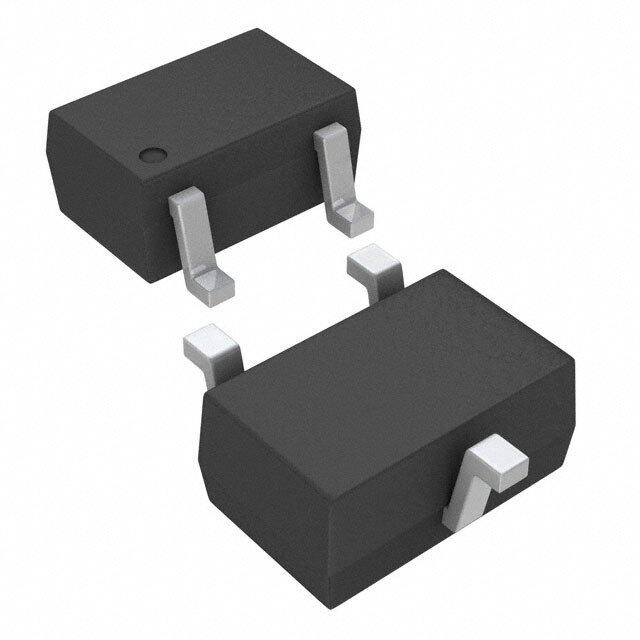
| 产品图片 |
|
| rohs | 符合RoHS无铅 / 符合限制有害物质指令(RoHS)规范要求 |
| 产品系列 | 电源管理 IC,参考电压,Texas Instruments LM431BCM3X/NOPB- |
| 数据手册 | |
| 产品型号 | LM431BCM3X/NOPB |
| RoHS指令信息 | |
| 串联VREF—输入电压—最大值 | 37 V |
| 产品种类 | 参考电压 |
| 供应商器件封装 | SOT-23-3 |
| 其它名称 | *LM431BCM3X/NOPB |
| 分流电流—最大值 | 100 mA |
| 分流电流—最小值 | 1 mA |
| 初始准确度 | 1 % |
| 包装 | 剪切带 (CT) |
| 参考类型 | Shunt Adjustable References |
| 商标 | Texas Instruments |
| 安装类型 | 表面贴装 |
| 安装风格 | SMD/SMT |
| 容差 | ±1% |
| 封装 | Reel |
| 封装/外壳 | TO-236-3,SC-59,SOT-23-3 |
| 封装/箱体 | SOT-23 |
| 工作温度 | 0°C ~ 70°C |
| 工厂包装数量 | 3000 |
| 平均温度系数—典型值 | 50 PPM/C |
| 最大工作温度 | + 70 C |
| 最小工作温度 | 0 C |
| 标准包装 | 3,000 |
| 温度系数 | 标准值 50ppm/°C |
| 电压-输入 | - |
| 电压-输出 | 2.495 V ~ 37 V |
| 电流-输出 | 100mA |
| 电流-阴极 | 1mA |
| 电流-静态 | - |
| 系列 | LM431 |
| 设计资源 | http://www.digikey.com/product-highlights/cn/zh/texas-instruments-webench-design-center/3176 |
| 输出电压 | 2.495 V to 37 V |
| 通道数 | 1 |


- 商务部:美国ITC正式对集成电路等产品启动337调查
- 曝三星4nm工艺存在良率问题 高通将骁龙8 Gen1或转产台积电
- 太阳诱电将投资9.5亿元在常州建新厂生产MLCC 预计2023年完工
- 英特尔发布欧洲新工厂建设计划 深化IDM 2.0 战略
- 台积电先进制程称霸业界 有大客户加持明年业绩稳了
- 达到5530亿美元!SIA预计今年全球半导体销售额将创下新高
- 英特尔拟将自动驾驶子公司Mobileye上市 估值或超500亿美元
- 三星加码芯片和SET,合并消费电子和移动部门,撤换高东真等 CEO
- 三星电子宣布重大人事变动 还合并消费电子和移动部门
- 海关总署:前11个月进口集成电路产品价值2.52万亿元 增长14.8%


PDF Datasheet 数据手册内容提取
Product Sample & Technical Tools & Support & Folder Buy Documents Software Community LM431 SNVS020H–MAY2000–REVISEDJANUARY2016 LM431 Adjustable Precision Zener Shunt Regulator 1 Features 3 Description • AverageTemperatureCoefficient50ppm/°C The LM431 is a 3-terminal adjustable shunt regulator 1 with ensured temperature stability over the entire • TemperatureCompensatedforOperationOver temperature range of operation. The output voltage theFullTemperatureRange may be set at any level greater than 2.5 V (V ) up REF • ProgrammableOutputVoltage to 36 V merely by selecting two external resistors that • FastTurnonResponse act as a voltage divided network. Due to the sharp turnon characteristics this device is an excellent • Low-OutputNoise replacementformanyZenerdiodeapplications. • Low-DynamicOutputImpedance The LM431 is available in space-saving SOIC-8, • AvailableinSpace-SavingSOIC-8,SOT-23,and SOT-23,andTO-92packages. TO-92Packages DeviceInformation(1) 2 Applications PARTNUMBER PACKAGE BODYSIZE(NOM) • AdjustableVoltageorCurrentLinearand SOIC(8) 4.90mm×3.91mm SwitchingPowerSupplies LM431 SOT-23(3) 2.92mm×1.30mm • VoltageMonitoring TO-92(3) 4.30mm×4.30mm • CurrentSourceandSinkCircuits (1) For all available packages, see the orderable addendum at • CircuitsRequiringPrecisionReferences theendofthedatasheet. • ZenerDiodeReplacements LM431Symbol FunctionalBlockDiagram 1 An IMPORTANT NOTICE at the end of this data sheet addresses availability, warranty, changes, use in safety-critical applications, intellectualpropertymattersandotherimportantdisclaimers.PRODUCTIONDATA.
LM431 SNVS020H–MAY2000–REVISEDJANUARY2016 www.ti.com Table of Contents 1 Features.................................................................. 1 8.3 FeatureDescription.................................................10 2 Applications........................................................... 1 8.4 DeviceFunctionalModes........................................11 3 Description............................................................. 1 9 ApplicationandImplementation........................ 12 4 RevisionHistory..................................................... 2 9.1 ApplicationInformation............................................12 9.2 TypicalApplications................................................13 5 PinConfigurationandFunctions......................... 3 10 PowerSupplyRecommendations..................... 19 6 Specifications......................................................... 4 11 Layout................................................................... 19 6.1 AbsoluteMaximumRatings......................................4 6.2 ESDRatings..............................................................4 11.1 LayoutGuidelines.................................................19 6.3 RecommendedOperatingConditions.......................4 11.2 LayoutExample....................................................19 6.4 ThermalInformation..................................................4 12 DeviceandDocumentationSupport................. 20 6.5 ElectricalCharacteristics...........................................5 12.1 CommunityResources..........................................20 6.6 TypicalCharacteristics..............................................7 12.2 Trademarks...........................................................20 7 ParameterMeasurementInformation..................7 12.3 ElectrostaticDischargeCaution............................20 12.4 Glossary................................................................20 8 DetailedDescription............................................ 10 13 Mechanical,Packaging,andOrderable 8.1 Overview.................................................................10 Information........................................................... 20 8.2 FunctionalBlockDiagram ......................................10 4 Revision History NOTE:Pagenumbersforpreviousrevisionsmaydifferfrompagenumbersinthecurrentversion. ChangesfromRevisionG(March2013)toRevisionH Page • AddedESDRatingstable,FeatureDescriptionsection,DeviceFunctionalModes,ApplicationandImplementation section,PowerSupplyRecommendationssection,Layoutsection,DeviceandDocumentationSupportsection,and Mechanical,Packaging,andOrderableInformationsection.................................................................................................. 1 ChangesfromRevisionF(April2013)toRevisionG Page • ChangedlayoutofNationalDataSheettoTIformat........................................................................................................... 18 2 SubmitDocumentationFeedback Copyright©2000–2016,TexasInstrumentsIncorporated ProductFolderLinks:LM431
LM431 www.ti.com SNVS020H–MAY2000–REVISEDJANUARY2016 5 Pin Configuration and Functions DPackage 8-PinSOIC DBZPackage TopView 3-PinSOT-23 TopView Note:NC=Notinternallyconnected. LPPackage 3-PinTO-92 TopView PinFunctions PIN I/O DESCRIPTION NAME SOIC SOT-23 TO-92 Anode 2,3,6,7 3 3 O Anodepin,normallygrounded Cathode 1 1 1 I/O Shuntcurrent/outputvoltage NC 4,5 — — — Noconnect Reference 8 2 2 I Referencepinforadjustableoutputvoltage Copyright©2000–2016,TexasInstrumentsIncorporated SubmitDocumentationFeedback 3 ProductFolderLinks:LM431
LM431 SNVS020H–MAY2000–REVISEDJANUARY2016 www.ti.com 6 Specifications 6.1 Absolute Maximum Ratings overoperatingfree-airtemperaturerange(unlessotherwisenoted)(1)(2) MIN MAX UNIT Cathodevoltage 37 V Referencevoltage –0.5 V Continuouscathodecurrent –10 150 mA Referenceinputcurrent 10 mA TO-92package 0.78 W Internalpower dissipation(3)(4) SOICpackage 0.81 W SOT-23package 0.28 W Industrial(LM431xI) –40 85 °C Operatingtemperature Commercial(LM431xC) 0 70 °C Storagetemperature –65 150 °C (1) StressesbeyondthoselistedunderAbsoluteMaximumRatingsmaycausepermanentdamagetothedevice.Thesearestressratings only,whichdonotimplyfunctionaloperationofthedeviceattheseoranyotherconditionsbeyondthoseindicatedunderRecommended OperatingConditions.Exposuretoabsolute-maximum-ratedconditionsforextendedperiodsmayaffectdevicereliability. (2) IfMilitary/Aerospacespecifieddevicesarerequired,pleasecontacttheTISalesOffice/Distributorsforavailabilityandspecifications. (3) T =150°C. JMax (4) Ratingsapplytoambienttemperatureat25°C.Abovethistemperature,deratetheTO-92at6.2mW/°C,theSOICat6.5mW/°C,the SOT-23at2.2mW/°C. 6.2 ESD Ratings VALUE UNIT V Electrostaticdischarge Human-bodymodel(HBM),perANSI/ESDA/JEDECJS-001(1) ±2500 V (ESD) (1) JEDECdocumentJEP155statesthat500-VHBMallowssafemanufacturingwithastandardESDcontrolprocess. 6.3 Recommended Operating Conditions overoperatingfree-airtemperaturerange(unlessotherwisenoted) MIN MAX UNIT Cathodevoltage V 37 V REF Cathodecurrent 1 100 mA 6.4 Thermal Information LM431 THERMALMETRIC(1) D(SOIC) DBZ(SOT-23) LP(TO-92) UNIT 8PINS 3PINS 3PINS R Junction-to-ambientthermalresistance 126.9 267.7 162.4 °C/W θJA R Junction-to-case(top)thermalresistance 72.2 138.3 85.8 °C/W θJC(top) R Junction-to-boardthermalresistance 67.5 61 — °C/W θJB ψ Junction-to-topcharacterizationparameter 21.1 21.5 29.4 °C/W JT ψ Junction-to-boardcharacterizationparameter 67 60.1 141.5 °C/W JB R Junction-to-case(bottom)thermalresistance — — — °C/W θJC(bot) (1) Formoreinformationabouttraditionalandnewthermalmetrics,seetheSemiconductorandICPackageThermalMetricsapplication report,SPRA953. 4 SubmitDocumentationFeedback Copyright©2000–2016,TexasInstrumentsIncorporated ProductFolderLinks:LM431
LM431 www.ti.com SNVS020H–MAY2000–REVISEDJANUARY2016 6.5 Electrical Characteristics T =25°Cunlessotherwisespecified A PARAMETER TESTCONDITIONS MIN TYP MAX UNIT V =V ,I =10mA Z REF I 2.44 2.495 2.55 LM431A(Figure6) V =V ,I =10mA V Referencevoltage Z REF I 2.47 2.495 2.52 V REF LM431B(Figure6) V =V ,I =10mA Z REF I 2.485 2.5 2.51 LM431C(Figure6) Deviationofreferenceinputvoltage V =V ,I =10mA, VDEV overtemperature(1) TZ=fuRllErFangIe(Figure6) 8 17 mV A ΔVREF/ Ratioofthechangeinreferencevoltagetothe IZ=10mA VZfromVREFto10V −1.4 −2.7 mV/V ΔVZ changeincathodevoltage (Figure7) VZfrom10Vto36V −1 −2 R =10kΩ,R =∞,I =10mA I Referenceinputcurrent 1 2 I 2 4 μA REF (Figure7) Deviationofreferenceinputcurrent R =10kΩ,R =∞,I =10mA, ∝I 1 2 I 0.4 1.2 μA REF overtemperature T =fullrange(Figure7) A I Minimumcathodecurrentforregulation V =V (Figure6) 0.4 1 mA Z(MIN) Z REF I OFF-statecurrent V =36V,V =0V(Figure8) 0.3 1 μA Z(OFF) Z REF (1) Deviationofreferenceinputvoltage,V ,isdefinedasthemaximumvariationofthereferenceinputvoltageoverthefulltemperature DEV range. Theaveragetemperaturecoefficientofthereferenceinputvoltage,∝V ,isdefinedas: REF Where: T –T =fulltemperaturechange(0–70°C). 2 1 V canbepositiveornegativedependingonwhethertheslopeispositiveornegative. REF Example:V =8mV,V =2495mV,T –T =70°C,slopeispositive. DEV REF 2 1 Copyright©2000–2016,TexasInstrumentsIncorporated SubmitDocumentationFeedback 5 ProductFolderLinks:LM431
LM431 SNVS020H–MAY2000–REVISEDJANUARY2016 www.ti.com Electrical Characteristics (continued) T =25°Cunlessotherwisespecified A PARAMETER TESTCONDITIONS MIN TYP MAX UNIT V =V ,LM431A, Z REF 0.75 Frequency=0Hz(Figure6) r Dynamicoutputimpedance(2) Ω Z V =V ,LM431B,LM431C Z REF 0.5 Frequency=0Hz(Figure6) (2) Thedynamicoutputimpedance,r ,isdefinedas: Z Whenthedeviceisprogrammedwithtwoexternalresistors,R1andR2,(seeFigure7),thedynamicoutputimpedanceoftheoverall circuit,r ,isdefinedas: Z 6 SubmitDocumentationFeedback Copyright©2000–2016,TexasInstrumentsIncorporated ProductFolderLinks:LM431
LM431 www.ti.com SNVS020H–MAY2000–REVISEDJANUARY2016 6.6 Typical Characteristics Note: Theareasunderthecurvesrepresentconditionsthatmay causethedevicetooscillate.ForcurvesB,C,andD,R2andV+ wereadjustedtoestablishtheinitialV andI conditionswithC =0. Z Z L V+andC werethenadjustedtodeterminetherangesofstability. L Figure1.DynamicImpedancevsFrequency Figure2.StabilityBoundaryConditions 7 Parameter Measurement Information Figure3. TestCircuitforDynamicImpedancevsFrequencyCurve Figure4. TestCircuitforCurveAAbove Copyright©2000–2016,TexasInstrumentsIncorporated SubmitDocumentationFeedback 7 ProductFolderLinks:LM431
LM431 SNVS020H–MAY2000–REVISEDJANUARY2016 www.ti.com Parameter Measurement Information (continued) Figure5. TestCircuitforCurvesB,CandDAbove Figure6. TestCircuitforV =V Z REF Note: V =V (1+R1/R2)+I ×R1 Z REF REF Figure7. TestCircuitforV >V Z REF 8 SubmitDocumentationFeedback Copyright©2000–2016,TexasInstrumentsIncorporated ProductFolderLinks:LM431
LM431 www.ti.com SNVS020H–MAY2000–REVISEDJANUARY2016 Parameter Measurement Information (continued) Figure8. TestCircuitforOFF-StateCurrent Copyright©2000–2016,TexasInstrumentsIncorporated SubmitDocumentationFeedback 9 ProductFolderLinks:LM431
LM431 SNVS020H–MAY2000–REVISEDJANUARY2016 www.ti.com 8 Detailed Description 8.1 Overview The LM431 is an adjustable precision shunt voltage regulator with ensured temperature stability over the entire temperature range. The part has three different packages available to meet small footprint requirements, and is availableinthreedifferenttolerancegrades. 8.2 Functional Block Diagram Figure9. LM431Symbol Figure10. LM431BlockDiagram 8.3 Feature Description The LM431 is a precision Zener diode. The part requires a small quiescent current for regulation, and regulates the output voltage by shunting more or less current to ground, depending on input voltage and load. The only external component requirement is a resistor between the cathode and the input voltage to set the input current. Anexternalcapacitorcanbeusedontheinputoroutput,butisnotrequired. 10 SubmitDocumentationFeedback Copyright©2000–2016,TexasInstrumentsIncorporated ProductFolderLinks:LM431
LM431 www.ti.com SNVS020H–MAY2000–REVISEDJANUARY2016 Feature Description (continued) Figure11. EquivalentCircuit 8.4 Device Functional Modes The LM431 is most commonly operated in closed-loop mode, where the reference node is tied to the output voltage via a resistor divider. The output voltage remains in regulation as long as I is between 1 mA and 100 z mA. The part can also be used in open-loop mode to act as a comparator, driving the feedback node from anothervoltagesource. Copyright©2000–2016,TexasInstrumentsIncorporated SubmitDocumentationFeedback 11 ProductFolderLinks:LM431
LM431 SNVS020H–MAY2000–REVISEDJANUARY2016 www.ti.com 9 Application and Implementation NOTE Information in the following applications sections is not part of the TI component specification, and TI does not warrant its accuracy or completeness. TI’s customers are responsible for determining suitability of components for their purposes. Customers must validateandtesttheirdesignimplementationtoconfirmsystemfunctionality. 9.1 Application Information The LM431 is an adjustable precision shunt voltage regulator with ensured temperature stability over the entire temperature range. For space critical applications, the LM431 is available in space saving SOIC-8, SOT-23 and TO-92packages.Theminimumoperatingcurrentis1mAwhilethemaximumoperatingcurrentis100mA. The typical thermal hysteresis specification is defined as the change in 25°C voltage measured after thermal cycling. The device is thermal cycled to temperature 0°C and then measured at 25°C. Next the device is thermal cycled to temperature 70°C and again measured at 25°C. The resulting VOUT delta shift between the 25°C measurements is thermal hysteresis. Thermal hysteresis is common in precision references and is induced by thermal-mechanical package stress. Changes in environmental storage temperature, operating temperature and boardmountingtemperatureareallfactorsthatcancontributetothermalhysteresis. In a conventional shunt regulator application (Figure 12), an external series resistor (R ) is connected between S the supply voltage and the LM431 cathode pin. R determines the current that flows through the load (I ) and S LOAD the LM431 (I ). Since load current and supply voltage may vary, R must be small enough to supply at least the Z S minimum acceptable I to the LM431 even when the supply voltage is at its minimum and the load current is at Z its maximum value. When the supply voltage is at its maximum and I is at its minimum, R must be large LOAD S enoughsothatthecurrentflowingthroughtheLM431islessthan100mA. R must be selected based on the supply voltage, (V+), the desired load and operating current, (I and I ), S LOAD Z andtheoutputvoltage,seeEquation1. V -V R = + O S I +I LOAD Z (1) The LM431 output voltage can be adjusted to any value in the range of 2.5 V through 37 V. It is a function of the internal reference voltage (VREF) and the ratio of the external feedback resistors as shown in Figure 12. The outputvoltageisfoundusingEquation2. V =V *(1+R /R ) O REF 1 2 where • V istheoutputvoltage(also,cathodevoltage,V ).TheactualvalueoftheinternalV isafunctionofV . (2) O Z REF Z ThecorrectedV isdeterminedbyEquation3: REF V =∆V *(∆V /∆V )+V REF Z REF Z Y where • V =2.5Vand∆V =(V –V ) Y Z Z Y • ΔV /ΔV isfoundintheElectricalCharacteristicsandistypically−1.4mV/VforV ragingfromV to10V REF Z Z REF and–1mV/VforV ragingfrom10Vto36V. (3) Z 12 SubmitDocumentationFeedback Copyright©2000–2016,TexasInstrumentsIncorporated ProductFolderLinks:LM431
LM431 www.ti.com SNVS020H–MAY2000–REVISEDJANUARY2016 9.2 Typical Applications 9.2.1 ShuntRegulator Figure12. ShuntRegulator 9.2.1.1 DesignRequirements Designashuntregulatorwiththefollowingrequirements: • V >V + O • V =5V O SelectR (aresistorbetweenV andV )suchthat:1mA< I <100mA S + O Z 9.2.1.2 DetailedDesignProcedure The resistor R must be selected such that current I remains in the operational region of the part for the entire S Z V range and load current range. The two extremes to consider are V at its minimum, and the load at its + + maximum, where R must be small enough for I to remain above 1 mA. The other extreme is V at its S Z + maximum, and the load at its minimum, where R must be large enough to maintain I < 100 mA. If unsure, try S Z using1mA≤ I ≤ 10mAasastartingpoint;justrememberthevalueofI varieswithinputvoltageandload. R Z UseEquation4andEquation5tosetR betweenR andR . S S_MIN S_MAX V -V R = +_MAX O S_MIN I +I LOAD_MIN Z_MAX (4) V -V R = +_MIN O S_MAX I +I LOAD_MAX Z_MIN (5) SetfeedbackresistorsR andR foraresistordividerbasedonEquation2andreproducedinEquation6 1 2 V =V *(1+R /R ) (6) O REF 1 2 So,fora5-Voutputvoltage,V ,andV of2.5V,simplecalculationyieldsR /R =1.Basedonthis,select O REF 1 2 R =1kΩandR2=1kΩ. 1 Copyright©2000–2016,TexasInstrumentsIncorporated SubmitDocumentationFeedback 13 ProductFolderLinks:LM431
LM431 SNVS020H–MAY2000–REVISEDJANUARY2016 www.ti.com Typical Applications (continued) 9.2.1.3 ApplicationCurves Figure13.InputCurrentvsV Figure14.ThermalInformation Z Figure15.InputCurrentvsV Z 9.2.2 OtherApplications Figure16. SingleSupplyComparatorWithTemperatureCompensatedThreshold 14 SubmitDocumentationFeedback Copyright©2000–2016,TexasInstrumentsIncorporated ProductFolderLinks:LM431
LM431 www.ti.com SNVS020H–MAY2000–REVISEDJANUARY2016 Typical Applications (continued) Figure17. SeriesRegulator Figure18. OutputControlofaThreeTerminalFixedRegulator Copyright©2000–2016,TexasInstrumentsIncorporated SubmitDocumentationFeedback 15 ProductFolderLinks:LM431
LM431 SNVS020H–MAY2000–REVISEDJANUARY2016 www.ti.com Typical Applications (continued) Figure19. HigherCurrentShuntRegulator Figure20. CrowBar 16 SubmitDocumentationFeedback Copyright©2000–2016,TexasInstrumentsIncorporated ProductFolderLinks:LM431
LM431 www.ti.com SNVS020H–MAY2000–REVISEDJANUARY2016 Typical Applications (continued) Figure21. OverVoltageandUnderVoltageProtectionCircuit Figure22. VoltageMonitor Copyright©2000–2016,TexasInstrumentsIncorporated SubmitDocumentationFeedback 17 ProductFolderLinks:LM431
LM431 SNVS020H–MAY2000–REVISEDJANUARY2016 www.ti.com Typical Applications (continued) Figure23. DelayTimer Figure24. CurrentLimiterorCurrentSource Figure25. ConstantCurrentSink 18 SubmitDocumentationFeedback Copyright©2000–2016,TexasInstrumentsIncorporated ProductFolderLinks:LM431
LM431 www.ti.com SNVS020H–MAY2000–REVISEDJANUARY2016 10 Power Supply Recommendations While a bypass capacitor is not required on the input voltage line, TI recommends reducing noise on the input whichcouldaffecttheoutput.TIrecommendsa0.1-µFceramiccapacitororlarger. 11 Layout 11.1 Layout Guidelines Place external components as close to the device as possible. Place R close to the cathode, as well as the S inputbypasscapacitor,ifused.Keepfeedbackresistorclosethedevicewheneverpossible. 11.2 Layout Example R physically close to device cathode S C physically close to device C physically close to device IN OUT Figure26. LM431LayoutRecommendation Copyright©2000–2016,TexasInstrumentsIncorporated SubmitDocumentationFeedback 19 ProductFolderLinks:LM431
LM431 SNVS020H–MAY2000–REVISEDJANUARY2016 www.ti.com 12 Device and Documentation Support 12.1 Community Resources The following links connect to TI community resources. Linked contents are provided "AS IS" by the respective contributors. They do not constitute TI specifications and do not necessarily reflect TI's views; see TI's Terms of Use. TIE2E™OnlineCommunity TI'sEngineer-to-Engineer(E2E)Community.Createdtofostercollaboration amongengineers.Ate2e.ti.com,youcanaskquestions,shareknowledge,exploreideasandhelp solveproblemswithfellowengineers. DesignSupport TI'sDesignSupport QuicklyfindhelpfulE2Eforumsalongwithdesignsupporttoolsand contactinformationfortechnicalsupport. 12.2 Trademarks E2EisatrademarkofTexasInstruments. Allothertrademarksarethepropertyoftheirrespectiveowners. 12.3 Electrostatic Discharge Caution Thesedeviceshavelimitedbuilt-inESDprotection.Theleadsshouldbeshortedtogetherorthedeviceplacedinconductivefoam duringstorageorhandlingtopreventelectrostaticdamagetotheMOSgates. 12.4 Glossary SLYZ022—TIGlossary. Thisglossarylistsandexplainsterms,acronyms,anddefinitions. 13 Mechanical, Packaging, and Orderable Information The following pages include mechanical, packaging, and orderable information. This information is the most current data available for the designated devices. This data is subject to change without notice and revision of thisdocument.Forbrowser-basedversionsofthisdatasheet,refertotheleft-handnavigation. 20 SubmitDocumentationFeedback Copyright©2000–2016,TexasInstrumentsIncorporated ProductFolderLinks:LM431
PACKAGE OPTION ADDENDUM www.ti.com 25-Jun-2016 PACKAGING INFORMATION Orderable Device Status Package Type Package Pins Package Eco Plan Lead/Ball Finish MSL Peak Temp Op Temp (°C) Device Marking Samples (1) Drawing Qty (2) (6) (3) (4/5) LM431ACM NRND SOIC D 8 95 TBD Call TI Call TI 0 to 70 LM431 ACM LM431ACM/NOPB ACTIVE SOIC D 8 95 Green (RoHS CU SN Level-1-260C-UNLIM 0 to 70 LM431 & no Sb/Br) ACM LM431ACM3/NOPB ACTIVE SOT-23 DBZ 3 1000 Green (RoHS CU SN Level-1-260C-UNLIM 0 to 70 N1F & no Sb/Br) LM431ACM3X NRND SOT-23 DBZ 3 3000 TBD Call TI Call TI 0 to 70 N1F LM431ACM3X/NOPB ACTIVE SOT-23 DBZ 3 3000 Green (RoHS CU SN Level-1-260C-UNLIM 0 to 70 N1F & no Sb/Br) LM431ACMX/NOPB ACTIVE SOIC D 8 2500 Green (RoHS CU SN Level-1-260C-UNLIM 0 to 70 LM431 & no Sb/Br) ACM LM431ACZ/LFT3 ACTIVE TO-92 LP 3 2000 Green (RoHS CU SN N / A for Pkg Type LM431 & no Sb/Br) ACZ LM431ACZ/LFT4 ACTIVE TO-92 LP 3 2000 Green (RoHS CU SN N / A for Pkg Type LM431 & no Sb/Br) ACZ LM431ACZ/NOPB ACTIVE TO-92 LP 3 1800 Green (RoHS CU SN N / A for Pkg Type 0 to 70 LM431 & no Sb/Br) ACZ LM431AIM NRND SOIC D 8 95 TBD Call TI Call TI -40 to 85 LM431 AIM LM431AIM/NOPB ACTIVE SOIC D 8 95 Green (RoHS CU SN Level-1-260C-UNLIM -40 to 85 LM431 & no Sb/Br) AIM LM431AIM3 NRND SOT-23 DBZ 3 1000 TBD Call TI Call TI -40 to 85 N1E LM431AIM3/NOPB ACTIVE SOT-23 DBZ 3 1000 Green (RoHS CU SN Level-1-260C-UNLIM -40 to 85 N1E & no Sb/Br) LM431AIM3X/NOPB ACTIVE SOT-23 DBZ 3 3000 Green (RoHS CU SN Level-1-260C-UNLIM -40 to 85 N1E & no Sb/Br) LM431AIMX/NOPB ACTIVE SOIC D 8 2500 Green (RoHS CU SN Level-1-260C-UNLIM -40 to 85 LM431 & no Sb/Br) AIM LM431AIZ/LFT1 ACTIVE TO-92 LP 3 2000 Green (RoHS CU SN N / A for Pkg Type LM431 & no Sb/Br) AIZ LM431AIZ/NOPB ACTIVE TO-92 LP 3 1800 Green (RoHS CU SN N / A for Pkg Type -40 to 85 LM431 & no Sb/Br) AIZ LM431BCM/NOPB ACTIVE SOIC D 8 95 Green (RoHS CU SN Level-1-260C-UNLIM 0 to 70 431 & no Sb/Br) BCM Addendum-Page 1
PACKAGE OPTION ADDENDUM www.ti.com 25-Jun-2016 Orderable Device Status Package Type Package Pins Package Eco Plan Lead/Ball Finish MSL Peak Temp Op Temp (°C) Device Marking Samples (1) Drawing Qty (2) (6) (3) (4/5) LM431BCM3 NRND SOT-23 DBZ 3 1000 TBD Call TI Call TI 0 to 70 N1D LM431BCM3/NOPB ACTIVE SOT-23 DBZ 3 1000 Green (RoHS CU SN Level-1-260C-UNLIM 0 to 70 N1D & no Sb/Br) LM431BCM3X/NOPB ACTIVE SOT-23 DBZ 3 3000 Green (RoHS CU SN Level-1-260C-UNLIM 0 to 70 N1D & no Sb/Br) LM431BCMX/NOPB ACTIVE SOIC D 8 2500 Green (RoHS CU SN Level-1-260C-UNLIM 0 to 70 431 & no Sb/Br) BCM LM431BCZ/NOPB ACTIVE TO-92 LP 3 1800 Green (RoHS CU SN N / A for Pkg Type 0 to 70 LM431 & no Sb/Br) BCZ LM431BIM NRND SOIC D 8 95 TBD Call TI Call TI -40 to 85 431 BIM LM431BIM/NOPB ACTIVE SOIC D 8 95 Green (RoHS CU SN Level-1-260C-UNLIM -40 to 85 431 & no Sb/Br) BIM LM431BIM3 NRND SOT-23 DBZ 3 1000 TBD Call TI Call TI -40 to 85 N1C LM431BIM3/NOPB ACTIVE SOT-23 DBZ 3 1000 Green (RoHS CU SN Level-1-260C-UNLIM -40 to 85 N1C & no Sb/Br) LM431BIM3X NRND SOT-23 DBZ 3 3000 TBD Call TI Call TI -40 to 85 N1C LM431BIM3X/NOPB ACTIVE SOT-23 DBZ 3 3000 Green (RoHS CU SN Level-1-260C-UNLIM -40 to 85 N1C & no Sb/Br) LM431BIMX/NOPB ACTIVE SOIC D 8 2500 Green (RoHS CU SN Level-1-260C-UNLIM -40 to 85 431 & no Sb/Br) BIM LM431CCM/NOPB ACTIVE SOIC D 8 95 Green (RoHS CU SN Level-1-260C-UNLIM 0 to 70 431 & no Sb/Br) CCM LM431CCM3/NOPB ACTIVE SOT-23 DBZ 3 1000 Green (RoHS CU SN Level-1-260C-UNLIM 0 to 70 N1B & no Sb/Br) LM431CCM3X NRND SOT-23 DBZ 3 3000 TBD Call TI Call TI 0 to 70 N1B LM431CCM3X/NOPB ACTIVE SOT-23 DBZ 3 3000 Green (RoHS CU SN Level-1-260C-UNLIM 0 to 70 N1B & no Sb/Br) LM431CCZ/NOPB ACTIVE TO-92 LP 3 1800 Green (RoHS CU SN N / A for Pkg Type 0 to 70 LM431 & no Sb/Br) CCZ LM431CIM NRND SOIC D 8 95 TBD Call TI Call TI -40 to 85 431 CIM LM431CIM/NOPB ACTIVE SOIC D 8 95 Green (RoHS CU SN Level-1-260C-UNLIM -40 to 85 431 & no Sb/Br) CIM LM431CIM3 NRND SOT-23 DBZ 3 1000 TBD Call TI Call TI -40 to 85 N1A Addendum-Page 2
PACKAGE OPTION ADDENDUM www.ti.com 25-Jun-2016 Orderable Device Status Package Type Package Pins Package Eco Plan Lead/Ball Finish MSL Peak Temp Op Temp (°C) Device Marking Samples (1) Drawing Qty (2) (6) (3) (4/5) LM431CIM3/NOPB ACTIVE SOT-23 DBZ 3 1000 Green (RoHS CU SN Level-1-260C-UNLIM -40 to 85 N1A & no Sb/Br) LM431CIM3X NRND SOT-23 DBZ 3 3000 TBD Call TI Call TI -40 to 85 N1A LM431CIM3X/NOPB ACTIVE SOT-23 DBZ 3 3000 Green (RoHS CU SN Level-1-260C-UNLIM -40 to 85 N1A & no Sb/Br) LM431CIZ/NOPB ACTIVE TO-92 LP 3 1800 Green (RoHS CU SN N / A for Pkg Type -40 to 85 LM431 & no Sb/Br) CIZ (1) The marketing status values are defined as follows: ACTIVE: Product device recommended for new designs. LIFEBUY: TI has announced that the device will be discontinued, and a lifetime-buy period is in effect. NRND: Not recommended for new designs. Device is in production to support existing customers, but TI does not recommend using this part in a new design. PREVIEW: Device has been announced but is not in production. Samples may or may not be available. OBSOLETE: TI has discontinued the production of the device. (2) Eco Plan - The planned eco-friendly classification: Pb-Free (RoHS), Pb-Free (RoHS Exempt), or Green (RoHS & no Sb/Br) - please check http://www.ti.com/productcontent for the latest availability information and additional product content details. TBD: The Pb-Free/Green conversion plan has not been defined. Pb-Free (RoHS): TI's terms "Lead-Free" or "Pb-Free" mean semiconductor products that are compatible with the current RoHS requirements for all 6 substances, including the requirement that lead not exceed 0.1% by weight in homogeneous materials. Where designed to be soldered at high temperatures, TI Pb-Free products are suitable for use in specified lead-free processes. Pb-Free (RoHS Exempt): This component has a RoHS exemption for either 1) lead-based flip-chip solder bumps used between the die and package, or 2) lead-based die adhesive used between the die and leadframe. The component is otherwise considered Pb-Free (RoHS compatible) as defined above. Green (RoHS & no Sb/Br): TI defines "Green" to mean Pb-Free (RoHS compatible), and free of Bromine (Br) and Antimony (Sb) based flame retardants (Br or Sb do not exceed 0.1% by weight in homogeneous material) (3) MSL, Peak Temp. - The Moisture Sensitivity Level rating according to the JEDEC industry standard classifications, and peak solder temperature. (4) There may be additional marking, which relates to the logo, the lot trace code information, or the environmental category on the device. (5) Multiple Device Markings will be inside parentheses. Only one Device Marking contained in parentheses and separated by a "~" will appear on a device. If a line is indented then it is a continuation of the previous line and the two combined represent the entire Device Marking for that device. (6) Lead/Ball Finish - Orderable Devices may have multiple material finish options. Finish options are separated by a vertical ruled line. Lead/Ball Finish values may wrap to two lines if the finish value exceeds the maximum column width. Important Information and Disclaimer:The information provided on this page represents TI's knowledge and belief as of the date that it is provided. TI bases its knowledge and belief on information provided by third parties, and makes no representation or warranty as to the accuracy of such information. Efforts are underway to better integrate information from third parties. TI has taken and Addendum-Page 3
PACKAGE OPTION ADDENDUM www.ti.com 25-Jun-2016 continues to take reasonable steps to provide representative and accurate information but may not have conducted destructive testing or chemical analysis on incoming materials and chemicals. TI and TI suppliers consider certain information to be proprietary, and thus CAS numbers and other limited information may not be available for release. In no event shall TI's liability arising out of such information exceed the total purchase price of the TI part(s) at issue in this document sold by TI to Customer on an annual basis. Addendum-Page 4
PACKAGE MATERIALS INFORMATION www.ti.com 3-Nov-2015 TAPE AND REEL INFORMATION *Alldimensionsarenominal Device Package Package Pins SPQ Reel Reel A0 B0 K0 P1 W Pin1 Type Drawing Diameter Width (mm) (mm) (mm) (mm) (mm) Quadrant (mm) W1(mm) LM431ACM3/NOPB SOT-23 DBZ 3 1000 178.0 8.4 3.3 2.9 1.22 4.0 8.0 Q3 LM431ACM3X SOT-23 DBZ 3 3000 178.0 8.4 3.3 2.9 1.22 4.0 8.0 Q3 LM431ACM3X/NOPB SOT-23 DBZ 3 3000 178.0 8.4 3.3 2.9 1.22 4.0 8.0 Q3 LM431ACMX/NOPB SOIC D 8 2500 330.0 12.4 6.5 5.4 2.0 8.0 12.0 Q1 LM431AIM3 SOT-23 DBZ 3 1000 178.0 8.4 3.3 2.9 1.22 4.0 8.0 Q3 LM431AIM3/NOPB SOT-23 DBZ 3 1000 178.0 8.4 3.3 2.9 1.22 4.0 8.0 Q3 LM431AIM3X/NOPB SOT-23 DBZ 3 3000 178.0 8.4 3.3 2.9 1.22 4.0 8.0 Q3 LM431AIMX/NOPB SOIC D 8 2500 330.0 12.4 6.5 5.4 2.0 8.0 12.0 Q1 LM431BCM3 SOT-23 DBZ 3 1000 178.0 8.4 3.3 2.9 1.22 4.0 8.0 Q3 LM431BCM3/NOPB SOT-23 DBZ 3 1000 178.0 8.4 3.3 2.9 1.22 4.0 8.0 Q3 LM431BCM3X/NOPB SOT-23 DBZ 3 3000 178.0 8.4 3.3 2.9 1.22 4.0 8.0 Q3 LM431BCMX/NOPB SOIC D 8 2500 330.0 12.4 6.5 5.4 2.0 8.0 12.0 Q1 LM431BIM3 SOT-23 DBZ 3 1000 178.0 8.4 3.3 2.9 1.22 4.0 8.0 Q3 LM431BIM3/NOPB SOT-23 DBZ 3 1000 178.0 8.4 3.3 2.9 1.22 4.0 8.0 Q3 LM431BIM3X SOT-23 DBZ 3 3000 178.0 8.4 3.3 2.9 1.22 4.0 8.0 Q3 LM431BIM3X/NOPB SOT-23 DBZ 3 3000 178.0 8.4 3.3 2.9 1.22 4.0 8.0 Q3 LM431BIMX/NOPB SOIC D 8 2500 330.0 12.4 6.5 5.4 2.0 8.0 12.0 Q1 LM431CCM3/NOPB SOT-23 DBZ 3 1000 178.0 8.4 3.3 2.9 1.22 4.0 8.0 Q3 PackMaterials-Page1
PACKAGE MATERIALS INFORMATION www.ti.com 3-Nov-2015 Device Package Package Pins SPQ Reel Reel A0 B0 K0 P1 W Pin1 Type Drawing Diameter Width (mm) (mm) (mm) (mm) (mm) Quadrant (mm) W1(mm) LM431CCM3X SOT-23 DBZ 3 3000 178.0 8.4 3.3 2.9 1.22 4.0 8.0 Q3 LM431CCM3X/NOPB SOT-23 DBZ 3 3000 178.0 8.4 3.3 2.9 1.22 4.0 8.0 Q3 LM431CIM3 SOT-23 DBZ 3 1000 178.0 8.4 3.3 2.9 1.22 4.0 8.0 Q3 LM431CIM3/NOPB SOT-23 DBZ 3 1000 178.0 8.4 3.3 2.9 1.22 4.0 8.0 Q3 LM431CIM3X SOT-23 DBZ 3 3000 178.0 8.4 3.3 2.9 1.22 4.0 8.0 Q3 LM431CIM3X/NOPB SOT-23 DBZ 3 3000 178.0 8.4 3.3 2.9 1.22 4.0 8.0 Q3 *Alldimensionsarenominal Device PackageType PackageDrawing Pins SPQ Length(mm) Width(mm) Height(mm) LM431ACM3/NOPB SOT-23 DBZ 3 1000 210.0 185.0 35.0 LM431ACM3X SOT-23 DBZ 3 3000 210.0 185.0 35.0 LM431ACM3X/NOPB SOT-23 DBZ 3 3000 210.0 185.0 35.0 LM431ACMX/NOPB SOIC D 8 2500 367.0 367.0 35.0 LM431AIM3 SOT-23 DBZ 3 1000 210.0 185.0 35.0 LM431AIM3/NOPB SOT-23 DBZ 3 1000 210.0 185.0 35.0 LM431AIM3X/NOPB SOT-23 DBZ 3 3000 210.0 185.0 35.0 LM431AIMX/NOPB SOIC D 8 2500 367.0 367.0 35.0 LM431BCM3 SOT-23 DBZ 3 1000 210.0 185.0 35.0 LM431BCM3/NOPB SOT-23 DBZ 3 1000 210.0 185.0 35.0 LM431BCM3X/NOPB SOT-23 DBZ 3 3000 210.0 185.0 35.0 PackMaterials-Page2
PACKAGE MATERIALS INFORMATION www.ti.com 3-Nov-2015 Device PackageType PackageDrawing Pins SPQ Length(mm) Width(mm) Height(mm) LM431BCMX/NOPB SOIC D 8 2500 367.0 367.0 35.0 LM431BIM3 SOT-23 DBZ 3 1000 210.0 185.0 35.0 LM431BIM3/NOPB SOT-23 DBZ 3 1000 210.0 185.0 35.0 LM431BIM3X SOT-23 DBZ 3 3000 210.0 185.0 35.0 LM431BIM3X/NOPB SOT-23 DBZ 3 3000 210.0 185.0 35.0 LM431BIMX/NOPB SOIC D 8 2500 367.0 367.0 35.0 LM431CCM3/NOPB SOT-23 DBZ 3 1000 210.0 185.0 35.0 LM431CCM3X SOT-23 DBZ 3 3000 210.0 185.0 35.0 LM431CCM3X/NOPB SOT-23 DBZ 3 3000 210.0 185.0 35.0 LM431CIM3 SOT-23 DBZ 3 1000 210.0 185.0 35.0 LM431CIM3/NOPB SOT-23 DBZ 3 1000 210.0 185.0 35.0 LM431CIM3X SOT-23 DBZ 3 3000 210.0 185.0 35.0 LM431CIM3X/NOPB SOT-23 DBZ 3 3000 210.0 185.0 35.0 PackMaterials-Page3
4203227/C
PACKAGE OUTLINE DBZ0003A SOT-23 - 1.12 mm max height SCALE 4.000 SMALL OUTLINE TRANSISTOR 2.64 C 2.10 1.12 MAX 1.4 1.2 B A 0.1 C PIN 1 INDEX AREA 1 0.95 3.04 1.9 2.80 3 2 0.5 3X 0.3 0.10 0.2 C A B (0.95) TYP 0.01 0.25 GAGE PLANE 0.20 TYP 0.08 0.6 TYP 0 -8 TYP 0.2 SEATING PLANE 4214838/C 04/2017 NOTES: 1. All linear dimensions are in millimeters. Any dimensions in parenthesis are for reference only. Dimensioning and tolerancing per ASME Y14.5M. 2. This drawing is subject to change without notice. 3. Reference JEDEC registration TO-236, except minimum foot length. www.ti.com
EXAMPLE BOARD LAYOUT DBZ0003A SOT-23 - 1.12 mm max height SMALL OUTLINE TRANSISTOR PKG 3X (1.3) 1 3X (0.6) SYMM 3 2X (0.95) 2 (R0.05) TYP (2.1) LAND PATTERN EXAMPLE SCALE:15X SOLDER MASK SOLDER MASK METAL UNDER METAL OPENING OPENING SOLDER MASK 0.07 MAX 0.07 MIN ALL AROUND ALL AROUND NON SOLDER MASK SOLDER MASK DEFINED DEFINED (PREFERRED) SOLDER MASK DETAILS 4214838/C 04/2017 NOTES: (continued) 4. Publication IPC-7351 may have alternate designs. 5. Solder mask tolerances between and around signal pads can vary based on board fabrication site. www.ti.com
EXAMPLE STENCIL DESIGN DBZ0003A SOT-23 - 1.12 mm max height SMALL OUTLINE TRANSISTOR PKG 3X (1.3) 1 3X (0.6) SYMM 3 2X(0.95) 2 (R0.05) TYP (2.1) SOLDER PASTE EXAMPLE BASED ON 0.125 THICK STENCIL SCALE:15X 4214838/C 04/2017 NOTES: (continued) 6. Laser cutting apertures with trapezoidal walls and rounded corners may offer better paste release. IPC-7525 may have alternate design recommendations. 7. Board assembly site may have different recommendations for stencil design. www.ti.com
None
None
PACKAGE OUTLINE LP0003A TO-92 - 5.34 mm max height SCALE 1.200 SCALE 1.200 TO-92 5.21 4.44 EJECTOR PIN OPTIONAL 5.34 4.32 (1.5) TYP (2.54) SEATING 2X NOTE 3 PLANE 4 MAX (0.51) TYP 6X 0.076 MAX SEATING PLANE 3X 12.7 MIN 0.43 2X 0.55 3X 3X 0.35 2.6 0.2 0.38 2X 1.27 0.13 FORMED LEAD OPTION OTHER DIMENSIONS IDENTICAL STRAIGHT LEAD OPTION TO STRAIGHT LEAD OPTION 2.67 3X 2.03 4.19 3.17 3 2 1 3.43 MIN 4215214/B 04/2017 NOTES: 1. All linear dimensions are in millimeters. Any dimensions in parenthesis are for reference only. Dimensioning and tolerancing per ASME Y14.5M. 2. This drawing is subject to change without notice. 3. Lead dimensions are not controlled within this area. 4. Reference JEDEC TO-226, variation AA. 5. Shipping method: a. Straight lead option available in bulk pack only. b. Formed lead option available in tape and reel or ammo pack. c. Specific products can be offered in limited combinations of shipping medium and lead options. d. Consult product folder for more information on available options. www.ti.com
EXAMPLE BOARD LAYOUT LP0003A TO-92 - 5.34 mm max height TO-92 FULL R TYP 0.05 MAX (1.07) ALL AROUND METAL 3X ( 0.85) HOLE TYP TYP 2X METAL (1.5) 2X (1.5) 2X SOLDER MASK OPENING 1 2 3 (R0.05) TYP 2X (1.07) (1.27) SOLDER MASK (2.54) OPENING LAND PATTERN EXAMPLE STRAIGHT LEAD OPTION NON-SOLDER MASK DEFINED SCALE:15X 0.05 MAX ( 1.4) 2X ( 1.4) ALL AROUND METAL TYP 3X ( 0.9) HOLE METAL 2X (R0.05) TYP 1 2 3 SOLDER MASK OPENING (2.6) SOLDER MASK OPENING (5.2) LAND PATTERN EXAMPLE FORMED LEAD OPTION NON-SOLDER MASK DEFINED SCALE:15X 4215214/B 04/2017 www.ti.com
TAPE SPECIFICATIONS LP0003A TO-92 - 5.34 mm max height TO-92 13.7 11.7 32 23 (2.5) TYP 0.5 MIN 16.5 15.5 11.0 9.75 8.5 8.50 19.0 17.5 2.9 6.75 3.7-4.3 TYP TYP 2.4 5.95 13.0 12.4 FOR FORMED LEAD OPTION PACKAGE 4215214/B 04/2017 www.ti.com
IMPORTANTNOTICE TexasInstrumentsIncorporated(TI)reservestherighttomakecorrections,enhancements,improvementsandotherchangestoits semiconductorproductsandservicesperJESD46,latestissue,andtodiscontinueanyproductorserviceperJESD48,latestissue.Buyers shouldobtainthelatestrelevantinformationbeforeplacingordersandshouldverifythatsuchinformationiscurrentandcomplete. TI’spublishedtermsofsaleforsemiconductorproducts(http://www.ti.com/sc/docs/stdterms.htm)applytothesaleofpackagedintegrated circuitproductsthatTIhasqualifiedandreleasedtomarket.AdditionaltermsmayapplytotheuseorsaleofothertypesofTIproductsand services. ReproductionofsignificantportionsofTIinformationinTIdatasheetsispermissibleonlyifreproductioniswithoutalterationandis accompaniedbyallassociatedwarranties,conditions,limitations,andnotices.TIisnotresponsibleorliableforsuchreproduced documentation.Informationofthirdpartiesmaybesubjecttoadditionalrestrictions.ResaleofTIproductsorserviceswithstatements differentfromorbeyondtheparametersstatedbyTIforthatproductorservicevoidsallexpressandanyimpliedwarrantiesforthe associatedTIproductorserviceandisanunfairanddeceptivebusinesspractice.TIisnotresponsibleorliableforanysuchstatements. BuyersandotherswhoaredevelopingsystemsthatincorporateTIproducts(collectively,“Designers”)understandandagreethatDesigners remainresponsibleforusingtheirindependentanalysis,evaluationandjudgmentindesigningtheirapplicationsandthatDesignershave fullandexclusiveresponsibilitytoassurethesafetyofDesigners'applicationsandcomplianceoftheirapplications(andofallTIproducts usedinorforDesigners’applications)withallapplicableregulations,lawsandotherapplicablerequirements.Designerrepresentsthat,with respecttotheirapplications,Designerhasallthenecessaryexpertisetocreateandimplementsafeguardsthat(1)anticipatedangerous consequencesoffailures,(2)monitorfailuresandtheirconsequences,and(3)lessenthelikelihoodoffailuresthatmightcauseharmand takeappropriateactions.DesigneragreesthatpriortousingordistributinganyapplicationsthatincludeTIproducts,Designerwill thoroughlytestsuchapplicationsandthefunctionalityofsuchTIproductsasusedinsuchapplications. TI’sprovisionoftechnical,applicationorotherdesignadvice,qualitycharacterization,reliabilitydataorotherservicesorinformation, including,butnotlimitedto,referencedesignsandmaterialsrelatingtoevaluationmodules,(collectively,“TIResources”)areintendedto assistdesignerswhoaredevelopingapplicationsthatincorporateTIproducts;bydownloading,accessingorusingTIResourcesinany way,Designer(individuallyor,ifDesignerisactingonbehalfofacompany,Designer’scompany)agreestouseanyparticularTIResource solelyforthispurposeandsubjecttothetermsofthisNotice. TI’sprovisionofTIResourcesdoesnotexpandorotherwisealterTI’sapplicablepublishedwarrantiesorwarrantydisclaimersforTI products,andnoadditionalobligationsorliabilitiesarisefromTIprovidingsuchTIResources.TIreservestherighttomakecorrections, enhancements,improvementsandotherchangestoitsTIResources.TIhasnotconductedanytestingotherthanthatspecifically describedinthepublisheddocumentationforaparticularTIResource. Designerisauthorizedtouse,copyandmodifyanyindividualTIResourceonlyinconnectionwiththedevelopmentofapplicationsthat includetheTIproduct(s)identifiedinsuchTIResource.NOOTHERLICENSE,EXPRESSORIMPLIED,BYESTOPPELOROTHERWISE TOANYOTHERTIINTELLECTUALPROPERTYRIGHT,ANDNOLICENSETOANYTECHNOLOGYORINTELLECTUALPROPERTY RIGHTOFTIORANYTHIRDPARTYISGRANTEDHEREIN,includingbutnotlimitedtoanypatentright,copyright,maskworkright,or otherintellectualpropertyrightrelatingtoanycombination,machine,orprocessinwhichTIproductsorservicesareused.Information regardingorreferencingthird-partyproductsorservicesdoesnotconstitutealicensetousesuchproductsorservices,orawarrantyor endorsementthereof.UseofTIResourcesmayrequirealicensefromathirdpartyunderthepatentsorotherintellectualpropertyofthe thirdparty,oralicensefromTIunderthepatentsorotherintellectualpropertyofTI. TIRESOURCESAREPROVIDED“ASIS”ANDWITHALLFAULTS.TIDISCLAIMSALLOTHERWARRANTIESOR REPRESENTATIONS,EXPRESSORIMPLIED,REGARDINGRESOURCESORUSETHEREOF,INCLUDINGBUTNOTLIMITEDTO ACCURACYORCOMPLETENESS,TITLE,ANYEPIDEMICFAILUREWARRANTYANDANYIMPLIEDWARRANTIESOF MERCHANTABILITY,FITNESSFORAPARTICULARPURPOSE,ANDNON-INFRINGEMENTOFANYTHIRDPARTYINTELLECTUAL PROPERTYRIGHTS.TISHALLNOTBELIABLEFORANDSHALLNOTDEFENDORINDEMNIFYDESIGNERAGAINSTANYCLAIM, INCLUDINGBUTNOTLIMITEDTOANYINFRINGEMENTCLAIMTHATRELATESTOORISBASEDONANYCOMBINATIONOF PRODUCTSEVENIFDESCRIBEDINTIRESOURCESOROTHERWISE.INNOEVENTSHALLTIBELIABLEFORANYACTUAL, DIRECT,SPECIAL,COLLATERAL,INDIRECT,PUNITIVE,INCIDENTAL,CONSEQUENTIALOREXEMPLARYDAMAGESIN CONNECTIONWITHORARISINGOUTOFTIRESOURCESORUSETHEREOF,ANDREGARDLESSOFWHETHERTIHASBEEN ADVISEDOFTHEPOSSIBILITYOFSUCHDAMAGES. UnlessTIhasexplicitlydesignatedanindividualproductasmeetingtherequirementsofaparticularindustrystandard(e.g.,ISO/TS16949 andISO26262),TIisnotresponsibleforanyfailuretomeetsuchindustrystandardrequirements. WhereTIspecificallypromotesproductsasfacilitatingfunctionalsafetyorascompliantwithindustryfunctionalsafetystandards,such productsareintendedtohelpenablecustomerstodesignandcreatetheirownapplicationsthatmeetapplicablefunctionalsafetystandards andrequirements.Usingproductsinanapplicationdoesnotbyitselfestablishanysafetyfeaturesintheapplication.Designersmust ensurecompliancewithsafety-relatedrequirementsandstandardsapplicabletotheirapplications.DesignermaynotuseanyTIproductsin life-criticalmedicalequipmentunlessauthorizedofficersofthepartieshaveexecutedaspecialcontractspecificallygoverningsuchuse. Life-criticalmedicalequipmentismedicalequipmentwherefailureofsuchequipmentwouldcauseseriousbodilyinjuryordeath(e.g.,life support,pacemakers,defibrillators,heartpumps,neurostimulators,andimplantables).Suchequipmentincludes,withoutlimitation,all medicaldevicesidentifiedbytheU.S.FoodandDrugAdministrationasClassIIIdevicesandequivalentclassificationsoutsidetheU.S. TImayexpresslydesignatecertainproductsascompletingaparticularqualification(e.g.,Q100,MilitaryGrade,orEnhancedProduct). Designersagreethatithasthenecessaryexpertisetoselecttheproductwiththeappropriatequalificationdesignationfortheirapplications andthatproperproductselectionisatDesigners’ownrisk.Designersaresolelyresponsibleforcompliancewithalllegalandregulatory requirementsinconnectionwithsuchselection. DesignerwillfullyindemnifyTIanditsrepresentativesagainstanydamages,costs,losses,and/orliabilitiesarisingoutofDesigner’snon- compliancewiththetermsandprovisionsofthisNotice. MailingAddress:TexasInstruments,PostOfficeBox655303,Dallas,Texas75265 Copyright©2017,TexasInstrumentsIncorporated