ICGOO在线商城 > 集成电路(IC) > 接口 - 传感器和探测器接口 > XTR117AIDRBT
 Datasheet下载
- 型号: XTR117AIDRBT
- 制造商: Texas Instruments
- 库位|库存: xxxx|xxxx
- 要求:
| 数量阶梯 | 香港交货 | 国内含税 |
| +xxxx | $xxxx | ¥xxxx |
查看当月历史价格
查看今年历史价格
XTR117AIDRBT产品简介:
ICGOO电子元器件商城为您提供XTR117AIDRBT由Texas Instruments设计生产,在icgoo商城现货销售,并且可以通过原厂、代理商等渠道进行代购。 XTR117AIDRBT价格参考。Texas InstrumentsXTR117AIDRBT封装/规格:接口 - 传感器和探测器接口, 。您可以下载XTR117AIDRBT参考资料、Datasheet数据手册功能说明书,资料中有XTR117AIDRBT 详细功能的应用电路图电压和使用方法及教程。
Texas Instruments(德州仪器)的XTR117AIDRBT是一款专门用于传感器和探测器接口的集成电路。其主要应用场景包括工业自动化、过程控制以及各种需要高精度电流信号传输的场合。

 应用场景:
1. 压力传感器接口:XTR117AIDRBT可以作为压力传感器的信号调理和传输接口,将传感器输出的微弱信号转换为标准的4-20mA电流信号,便于远距离传输和后续处理。

2. 温度传感器接口:在温度测量系统中,该芯片可用于连接热电偶、RTD(电阻温度检测器)等温度传感器,提供精确的信号放大和线性化处理。

3. 液位检测系统:用于液位传感器的数据采集与转换,能够将液位变化转化为标准化的电流信号输出,适用于化工、石油等行业。

4. 流量计配套使用:在流体流量监测设备中,配合涡街流量计或电磁流量计等,实现对流量数据的精确采集与远程传输。

5. 工业过程控制系统:作为工业自动化系统中的核心组件之一,负责将各种类型的传感器信号整合并转换成统一格式的电信号,供PLC(可编程逻辑控制器)或其他控制单元使用。

6. 气体浓度监测:可用于气体检测仪中,对接气体传感器进行信号处理,生成稳定的电流输出以反映气体浓度的变化。

总之,XTR117AIDRBT以其低功耗、高精度及良好的稳定性,广泛应用于需要可靠地将传感器信号转换为标准工业电流信号的各种领域,确保了信息传递的准确性与效率。
| 参数 | 数值 |
| 产品目录 | 集成电路 (IC)半导体 |
| 描述 | IC TX 4-20MA CURR-LOOP 8SON接口 - 专用 XTR117 4-20mA Crnt Loop Transmitter |
| 产品分类 | |
| 品牌 | Texas Instruments |
| 产品手册 | |
| 产品图片 |
|
| rohs | 符合RoHS无铅 / 符合限制有害物质指令(RoHS)规范要求 |
| 产品系列 | 接口 - 专用,Texas Instruments XTR117AIDRBT- |
| 数据手册 | |
| 产品型号 | XTR117AIDRBT |
| 产品种类 | |
| 产品类型 | Current Transmitter |
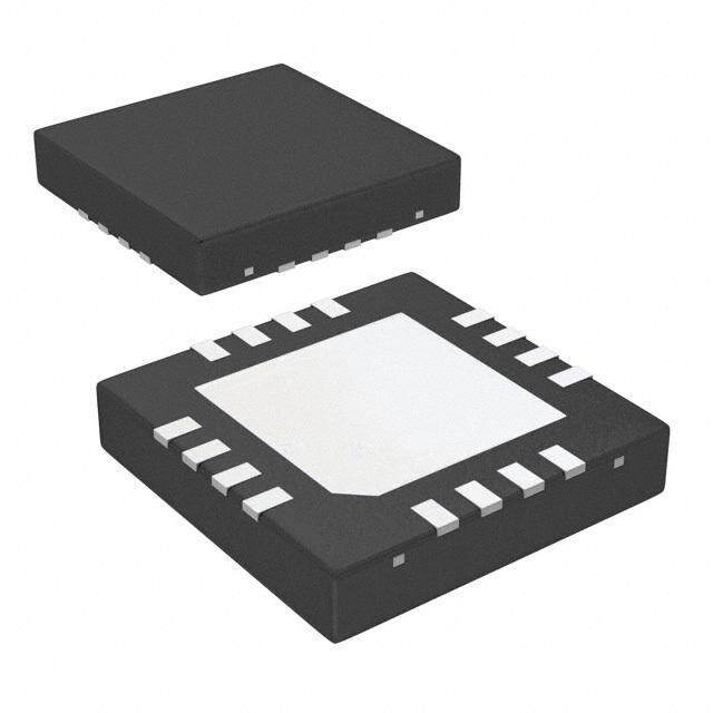
| 供应商器件封装 | 8-SON 裸露焊盘(3x3) |
| 其它名称 | 296-19487-2 |
| 包装 | 带卷 (TR) |
| 单位重量 | 24 mg |
| 商标 | Texas Instruments |
| 安装类型 | 表面贴装 |
| 安装风格 | SMD/SMT |
| 封装 | Reel |
| 封装/外壳 | 8-VDFN 裸露焊盘 |
| 封装/箱体 | VSON-8 |
| 工作电源电压 | 7.5 V to 40 V |
| 工厂包装数量 | 250 |
| 接口 | 2 线 |
| 描述/功能 | XTR117 4-20MA CURRENT LOOP TRANSMITTER |
| 最大工作温度 | + 125 C |
| 最小工作温度 | - 40 C |
| 标准包装 | 250 |
| 特色产品 | http://www.digikey.com/product-highlights/cn/zh/texas-instruments-chem-gas-sensor-solution/1191 |
| 电流-电源 | 20mA |
| 电源电压-最大 | 40 V |
| 电源电压-最小 | 7.5 V |
| 电源电流 | 130 uA |
| 类型 | 电流发送器 |
| 系列 | XTR117 |
| 输入电压 | 5 V |
| 输入类型 | 电压 |
| 输入补偿电压 | 100 uV |
| 输出电压 | 5 V |
| 输出类型 | 电压 |


- 商务部:美国ITC正式对集成电路等产品启动337调查
- 曝三星4nm工艺存在良率问题 高通将骁龙8 Gen1或转产台积电
- 太阳诱电将投资9.5亿元在常州建新厂生产MLCC 预计2023年完工
- 英特尔发布欧洲新工厂建设计划 深化IDM 2.0 战略
- 台积电先进制程称霸业界 有大客户加持明年业绩稳了
- 达到5530亿美元!SIA预计今年全球半导体销售额将创下新高
- 英特尔拟将自动驾驶子公司Mobileye上市 估值或超500亿美元
- 三星加码芯片和SET,合并消费电子和移动部门,撤换高东真等 CEO
- 三星电子宣布重大人事变动 还合并消费电子和移动部门
- 海关总署:前11个月进口集成电路产品价值2.52万亿元 增长14.8%


PDF Datasheet 数据手册内容提取
XTR117 SBOS344C − SEPTEMBER 2005 − REVISED MAY 2012 4-20mA Current-Loop Transmitter FEATURES DESCRIPTION (cid:2) LOW QUIESCENT CURRENT: 130μA The XTR117 is a precision current output converter designed (cid:2) 5V REGULATOR FOR EXTERNAL CIRCUITS to transmit analog 4-20mA signals over an industry-standard (cid:2) LOW SPAN ERROR: 0.05% current loop. It provides accurate current scaling and output (cid:2) LOW NONLINEARITY ERROR: 0.003% current limit functions. (cid:2) WIDE-LOOP SUPPLY RANGE: 7.5V to 40V The on-chip voltage regulator (5V) can be used to power (cid:2) MSOP-8 AND DFN-8 PACKAGES external circuitry. A current return pin (I ) senses any RET current used in external circuitry to assure an accurate APPLICATIONS control of the output current. (cid:2) The XTR117 is a fundamental building block of smart TWO-WIRE, 4-20mA CURRENT LOOP sensors using 4-20mA current transmission. The XTR117 is TRANSMITTER (cid:2) specified for operation over the extended industrial SMART TRANSMITTER temperature range, −40°C to +125°C. (cid:2) INDUSTRIAL PROCESS CONTROL (cid:2) TEST SYSTEMS (cid:2) CURRENT AMPLIFIER RELATED 4-20mA PRODUCTS (cid:2) VOLTAGE-TO-CURRENT AMPLIFIER XTR115 5V regulator output and 2.5V reference output XTR116 5V regulator output and 4.096V reference output NOTE: For 4-20mA complete bridge and RTO conditioner solutions, see the XTR product family website at www.ti.com. XTR117 I VREG +5V V+ O 8 Regulator 7 B Q1 6 R IN IIN VLOOP 2 A1 E V IN 5 R R L I LIM RET 3 R R IO=100VIN 1 2 2.475kΩ 25Ω RIN 4 Please be aware that an important notice concerning availability, standard warranty, and use in critical applications of TexasInstruments semiconductor products and disclaimers thereto appears at the end of this data sheet. All trademarks are the property of their respective owners. PRODUCTION DATA information is current as of publication date. Products Copyright © 2005−2006, Texas Instruments Incorporated conform to specifications per the terms of Texas Instruments standard warranty. Production processing does not necessarily include testing of all parameters. www.ti.com
XTR117 www.ti.com SBOS344C − SEPTEMBER 2005 − REVISED MAY 2012 ABSOLUTE MAXIMUM RATINGS(1) ELECTROSTATIC DISCHARGE SENSITIVITY Power Supply, V+ (referenced to I pin). . . . . . . . . . . . . . . . . +50V O This integrated circuit can be damaged by ESD. Texas Input Voltage, (referenced to I pin). . . . . . . . . . . . . . . . . 0V to V+ RET Instruments recommends that all integrated circuits be Output Current Limit . . . . . . . . . . . . . . . . . . . . . . . . . . . . Continuous handled with appropriate precautions. Failure to observe VREG, Short-Circuit . . . . . . . . . . . . . . . . . . . . . . . . . . . . . Continuous proper handling and installation procedures can cause damage. Operating Temperature Range . . . . . . . . . . . . . . . −55°C to +125°C Storage Temperature Range . . . . . . . . . . . . . . . . . −55°C to +150°C ESD damage can range from subtle performance degradation to Junction Temperature. . . . . . . . . . . . . . . . . . . . . . . . . . . . . . . +165°C complete device failure. Precision integrated circuits may be more ESD Rating (Human Body Model). . . . . . . . . . . . . . . . . . . . . . . 2000V susceptible to damage because very small parametric changes could cause the device not to meet its published specifications. (Charged Device Model) . . . . . . . . . . . . . . . . . 1000V (1) Stresses above these ratings may cause permanent damage. Exposure to absolute maximum conditions for extended periods may degrade device reliability. These are stress ratings only, and functional operation of the device at these or any other conditions beyond those specified is not implied. PACKAGE/ORDERING INFORMATION(1) PRODUCT PACKAGE-LEAD PACKAGE DESIGNATOR PACKAGE MARKING XXTTRR111177 MMSSOOPP-88 DDGGKK BBOOZZ XXTTRR111177 DDFFNN-88 DDRRBB BBOOYY (1) For the most current package and ordering information see the Package Option Addendum at the end of this document, or see the TI web site at www.ti.com. PIN ASSIGNMENTS Top View XTR117 XTR117 NC(1) 1 8 V NC(1) 1 8 V REG REG Exposed IIN 2 7 V+ IIN 2 Thermal 7 V+ DiePad IRET 3 6 B(Base) IRET 3 on 6 B(Base) Underside(2) IO 4 5 E(Emitter) IO 4 5 E(Emitter) MSOP−8 DFN−8 NOTES:(1)NC=Noconnection.LeaveunconnectedonPCB. (2)ConnectthermaldiepadtoI orleaveunconnectedonPCB. RET 2
XTR117 www.ti.com SBOS344C − SEPTEMBER 2005 − REVISED MAY 2012 ELECTRICAL CHARACTERISTICS: V+ = +24V Boldface limits apply over the temperature range, T = −40°C to +125°C. A All specifications at T = +25°C, V+ = 24V, R = 20kΩ, and TIP29C external transistor, unless otherwise noted. A IN XTR117 PARAMETER CONDITION MIN TYP MAX UNITS OUTPUT Output Current Equation IO IO = IIN x 100 Output Current, Linear Range 0.20 25 mA Over-Scale Limit ILIM 32 mA Under-Scale Limit IMIN IREG = 0 0.13 0.20 mA SPAN Span (Current Gain) S 100 A/A Error(1) IO = 200μA to 25mA ±0.05 ±0.4 % vs Temperature TA = −40°C to +125°C ±3 ±20 ppm/°C Nonlinearity IO = 200μA to 25mA ±0.003 ±0.02 % INPUT Offset Voltage (Op Amp) VOS IIN = 40μA ±100 ±500 μV vs Temperature TA = −40°C to +125°C ±0.7 ±6 μV/°C vs Supply Voltage, V+ V+ = 7.5V to 40V +0.1 +2 μV/V Bias Current IB −35 nA vs Temperature TA = −40°C to +125°C 150 pA/°C Noise: 0.1Hz to 10Hz en 0.6 μVPP DYNAMIC RESPONSE Small-Signal Bandwidth CLOOP = 0, RL = 0 380 kHz Slew Rate 3.2 mA/μs VREG(2) Voltage 5 V Voltage Accuracy IREG = 0 ±0.05 ±0.1 V vs Temperature TA = −40°C to +125°C ±0.1 mV/°C vs Supply Voltage, V+ V+ = 7.5V to 40V 1 mV/V vs Output Current See Typical Characteristics Short-Circuit Current 12 mA POWER SUPPLY Specified Voltage Range V+ +24 V Operating Voltage Range +7.5 +40 V Quiescent Current IQ 130 200 μA Over Temperature TA = −40°C to +125°C 250 μA TEMPERATURE RANGE Specified Range −40 +125 °C Operating Range −55 +125 °C Storage Range −55 +150 °C Thermal Resistance (cid:2)JA MSOP 150 °C/W DFN 53 °C/W (1) Does not include initial error or temperature coefficient of RIN. (2) Voltage measured with respect to IRET pin. 3
XTR117 www.ti.com SBOS344C − SEPTEMBER 2005 − REVISED MAY 2012 TYPICAL CHARACTERISTICS: V+ = +2.7V to +5.5V At T = +25°C, V+ = 24V, R = 20kΩ, and TIP29C external transistor, unless otherwise noted. A IN CURRENTGAINvsFREQUENCY QUIESCENTCURRENTvsTEMPERATURE 45 180 170 40 160 A) μnt( 150 V+=36V n(dB) 30 CROLU=T0=Ω0 Curre 114300 Gai ent 120 20 CROLUT==25100ΩnF Quiesc 110 V+=24V 100 V+=7.5V 90 10 80 10k 100k 1M −75 −50 −25 0 25 50 75 100 125 Frequency(Hz) Temperature((cid:3)C) OVER−SCALECURRENTvsTEMPERATURE VREGVOLTAGEvsVREGCURRENT 34 5.5 +125(cid:3)C WithExternalTransistor 33 A) −55(cid:3)C m nt( 32 (V) Curre 31 V+=36V oltage 5.0 +25(cid:3)C −55(cid:3)C ale V+=7.5V VG +25(cid:3)C −Sc 30 VRE er V+=24V v O Sinking Sourcing 29 Current Current +125(cid:3)C 28 4.5 −75 −50 −25 0 25 50 75 100 125 −1 0 1 2 3 4 Temperature((cid:3)C) IREGCurrent(mA) OFFSETVOLTAGEDISTRIBUTION SPANERRORvsTEMPERATURE 50 40 30 %) 20 n (m 10 atio nError −100 Popul a Sp −20 −30 −40 −50 000000000000000000000 −75 −50 −25 0 25 50 75 100 125 504540353025201510−5 5101520253035404550 −−−−−−−−− Temperature((cid:3)C) OffsetVoltage(μV) 4
XTR117 www.ti.com SBOS344C − SEPTEMBER 2005 − REVISED MAY 2012 APPLICATIONS INFORMATION EXTERNAL TRANSISTOR The external transistor, Q , conducts the majority of the BASIC OPERATION 1 full-scale output current. Power dissipation in this The XTR117 is a precision current output converter transistor can approach 0.8W with high loop voltage designed to transmit analog 4-20mA signals over an (40V) and 20mA output current. The XTR117 is industry-standard current loop. Figure 1 shows basic designed to use an external transistor to avoid on-chip, circuit connections with representative simplified input thermal-induced errors. Heat produced by Q will still 1 circuitry. The XTR117 is a two-wire current transmitter. cause ambient temperature changes that can influence Its input current (pin 2) controls the output current. A the XTR117 performance. To minimize these effects, portion of the output current flows into the V+ power locate Q away from sensitive analog circuitry, including 1 supply, pin 7. The remaining current flows in Q1. XTR117. Mount Q1 so that heat is conducted to the External input circuitry connected to the XTR117 can be outside of the transducer housing. powered from V . Current drawn from these REG The XTR117 is designed to use virtually any NPN terminals must be returned to I , pin 3. The I pin is RET RET transistor with sufficient voltage, current and power a local ground for input circuitry driving the XTR117. rating. Case style and thermal mounting considerations The XTR117 is a current-input device with a gain of 100. often influence the choice for any given application. A current flowing into pin 2 produces IO = 100 x IIN. The Several possible choices are listed in Figure 1. A input voltage at the IIN pin is zero (referred to the IRET MOSFET transistor will not improve the accuracy of the pin). A voltage input is converted to an input current with XTR117 and is not recommended. an external input resistor, R , as shown in Figure 1. IN Typical full-scale input voltages range from 1V and upward. Full-scale inputs greater than 0.5V are recommend to minimize the effects of offset voltage and drift of A1. Forimprovedprecisionuseanexternal voltagereference. PossiblechoicesforQ1(seetext): DEVICE VOLTAGE TYPE PACKAGE REF3140 4.096V MJE3440 SOT−32 REF3130 3.0V TIP41C TO−220 REF3125 2.5V MJD3340 D−PAK UseREF32xxforlowerdrift. (VREF) 5V IREG VREG XTR117 +5V V+ IO 8 Regulator 7 B Q1 6 Input VIN 2R0kINΩ IIN IIN VLOOP Circuitry 2 A1 COUT E 10nF 5 I RLIM RL RET 3 R R fArollmretIuRErnGcaunrdreIRnEtF 2.1475kΩ 252Ω IO 4 I=100(I ) IN Figure 1. Basic Circuit Connections 5
XTR117 www.ti.com SBOS344C − SEPTEMBER 2005 − REVISED MAY 2012 MINIMUM OUTPUT CURRENT MAXIMUM OUTPUT CURRENT The quiescent current of the XTR117 (typically 130μA) The XTR117 provides accurate, linear output up to is the lower limit of its output current. Zero input current 25mA. Internal circuitry limits the output current to (I = 0) will produce an I equal to the quiescent current. approximately 32mA to protect the transmitter and loop IN O Output current will not begin to increase until power/measurement circuitry. I > I /100. Current drawn from V will be added to IN Q REG It is possible to extend the output current range of the this minimum output current. Up to 3.8mA is available XTR117 by connecting an external resistor from pin 3 to power external circuitry while still allowing the output to pin 5, to change the current limit value. Since all current to go below 4mA. output current must flow through internal resistors, it is possible to cause internal damage with excessive current. Output currents greater than 45mA may cause OFFSETTING THE INPUT permanent damage. A low-scale output of 4mA is produced by creating a 40μA input current. This input current can be created REVERSE-VOLTAGE PROTECTION with the proper value resistor from an external reference voltage (V ) as shown in Figure 2. V REF REG The XTR117 low compliance voltage rating (minimum can be used as shown in Figure 2 but will not have the operating voltage) of 7.5V permits the use of various temperature stability of a high quality reference such as voltage protection methods without compromising the REF3125. operating range. Figure 3 shows a diode bridge circuit which allows normal operation even when the voltage connection lines are reversed. The bridge causes a two XTR117 VRE.F..(..2....5.V...)..o..r...VREG diode drop (approximately 1.4V) loss in loop supply 8 voltage. This voltage drop results in a compliance voltage of approximately 9V—satisfactory for most RIN 40μA 62.5kΩ applications. A diode can be inserted in series with the IIN loop supply voltage and the V+ pin to protect against 2 A1 reverse output connection lines with only a 0.7V loss in 0to160μA loop supply voltage. I RET 3 R 1 2.475kΩ Figure 2. Creating Low-Scale Offset XTR117 VREG +5V V+ 8 Regulator 7 MaximumV mustbeless B PS Q1 thanminimumvoltagerating 6 ofthezenerdiode. R IN I IN 2 A1 E 0.01μF D1(1) IN4148 V IN 5 I RLIM RL VLOOP RET 3 IO=100VIN R R 2.1475kΩ 252Ω RIN Thediodebridgecausesa 1.4Vlossinloopsupplyvoltage. 4 SeeReverse−VoltageProtection. NOTE:(1)Someexamplesofzenerdiodesinclude:P6KE51or1N4755A. Uselower voltagezenerdiodeswithlooppower−supply voltages <30Vforincreasedprotection.See Over−voltage Surge Protection. Figure 3. Reverse Voltage Operation and Over-Voltage Surge Protection 6
XTR117 www.ti.com SBOS344C − SEPTEMBER 2005 − REVISED MAY 2012 OVER-VOLTAGE SURGE PROTECTION protection diode is used, a series diode or diode bridge should be used for protection against reversed Remote connections to current transmitters can connections. sometimes be subjected to voltage surges. It is prudent to limit the maximum surge voltage applied to the XTR117 to as low as practical. Various zener diode and RADIO FREQUENCY INTERFERENCE surge clamping diodes are specially designed for this The long wire lengths of current loops invite radio purpose. Select a clamp diode with as low a voltage frequency (RF) interference. RF interference can be rating as possible for best protection. Absolute rectified by the input circuitry of the XTR117 or maximum power-supply rating on the XTR117 is preceding circuitry. This effect generally appears as an specified at +50V. Keep overvoltages and transients unstable output current that varies with the position of below +50V to ensure reliable operation when the loop supply or input wiring. Interference may also enter supply returns to normal (7.5V to 40V). at the input terminals. For integrated transmitter Most surge protection zener diodes have a diode assemblies with short connections to the sensor, the characteristic in the forward direction that will conduct interference more likely comes from the current loop excessive current, possibly damaging receiving-side connections. circuitry if the loop connections are reversed. If a surge V XTR117 REG 8 R VO IN IIN D/A 2 I RET 3 V XTR117 REG 8 Digital IO IIN Control D/A 2 Optical Isolation I RET 3 V XTR117 REG 8 R R CDoignittaroll μC POWuMt FILTER IN II2N Optical Isolation C FILTER I RET 3 Figure 4. Digital Control Methods 7
XTR117 www.ti.com SBOS344C − SEPTEMBER 2005 − REVISED MAY 2012 VS Nonlinear Linearization Ref 2.5V P 0psi50 TraBnrsiddguecer PGA309 Circuit LinDAC VREG XTR117 Re+g5uVlator 7V+ IO AnalogSensorLinearization 8 B MFoanuitlotr AutPoG−ZAero SOcvaeler/ULinmdieterr VLOinUeTa(1r)2R5kINΩ R12O5SIkI2NΩ A1 6 Q1 VLOOP AnalogSignalConditioning E +1−2450(cid:3)(cid:3)CC T ExtTemp DTCeiogmmitpapelernastuarteionIntTemp TAeDmCp InCtoenrftarocleRCeigrcisutietrry IRE3T R2.1475kΩ R252ΩRLIM 5IO=R10IN0VIN RL ExtTemp 4 EEPROM (SOT23−5) DigitalCalibration NOTE:(1)PGA309VOUT:0.5Vto4.5V. Figure 5. Complete 4-20mA Pressure Transducer Solution with PGA309 and XTR117 DFN PACKAGE LAYOUT GUIDELINES The XTR117 is offered in a DFN-8 package (also known The exposed leadframe die pad on the DFN package as SON). The DFN is a QFN package with lead contacts should be soldered to a thermal pad on the PCB. A on only two sides of the bottom of the package. This mechanical drawing showing an example layout is leadless package maximizes board space and attached at the end of this data sheet. Refinements to enhances thermal and electrical characteristics through this layout may be required based on assembly process an exposed pad. requirements. Mechanical drawings located at the end of this data sheet list the physical dimensions for the DFN packages are physically small, have a smaller package and pad. The five holes in the landing pattern routing area, improved thermal performance, and are optional, and are intended for use with thermal vias improved electrical parasitics. Additionally, the absence that connect the leadframe die pad to the heatsink area of external leads eliminates bent-lead issues. on the PCB. The DFN package can be easily mounted using Soldering the exposed pad significantly improves standard printed circuit board (PCB) assembly board-level reliability during temperature cycling, key techniques. See Application Note, QFN/SON PCB push, package shear, and similar board-level tests. Attachment (SLUA271) and Application Report, Quad Even with applications that have low power dissipation, Flatpack No-Lead Logic Packages (SCBA017), both the exposed pad must be soldered to the PCB to available for download at www.ti.com. provide structural integrity and long-term stability. The exposed leadframe die pad on the bottom of the package should be connected to I or left RET unconnected. 8
PACKAGE OPTION ADDENDUM www.ti.com 6-Feb-2020 PACKAGING INFORMATION Orderable Device Status Package Type Package Pins Package Eco Plan Lead/Ball Finish MSL Peak Temp Op Temp (°C) Device Marking Samples (1) Drawing Qty (2) (6) (3) (4/5) XTR117AIDGKR ACTIVE VSSOP DGK 8 2500 Green (RoHS NIPDAU | NIPDAUAG Level-3-260C-168 HR -40 to 125 BOZ & no Sb/Br) XTR117AIDGKRG4 ACTIVE VSSOP DGK 8 2500 Green (RoHS NIPDAUAG Level-3-260C-168 HR -40 to 125 BOZ & no Sb/Br) XTR117AIDGKT ACTIVE VSSOP DGK 8 250 Green (RoHS NIPDAU | NIPDAUAG Level-3-260C-168 HR -40 to 125 BOZ & no Sb/Br) XTR117AIDRBR ACTIVE SON DRB 8 3000 Green (RoHS NIPDAU Level-3-260C-168 HR -40 to 125 BOY & no Sb/Br) XTR117AIDRBT ACTIVE SON DRB 8 250 Green (RoHS NIPDAU Level-3-260C-168 HR -40 to 125 BOY & no Sb/Br) (1) The marketing status values are defined as follows: ACTIVE: Product device recommended for new designs. LIFEBUY: TI has announced that the device will be discontinued, and a lifetime-buy period is in effect. NRND: Not recommended for new designs. Device is in production to support existing customers, but TI does not recommend using this part in a new design. PREVIEW: Device has been announced but is not in production. Samples may or may not be available. OBSOLETE: TI has discontinued the production of the device. (2) RoHS: TI defines "RoHS" to mean semiconductor products that are compliant with the current EU RoHS requirements for all 10 RoHS substances, including the requirement that RoHS substance do not exceed 0.1% by weight in homogeneous materials. Where designed to be soldered at high temperatures, "RoHS" products are suitable for use in specified lead-free processes. TI may reference these types of products as "Pb-Free". RoHS Exempt: TI defines "RoHS Exempt" to mean products that contain lead but are compliant with EU RoHS pursuant to a specific EU RoHS exemption. Green: TI defines "Green" to mean the content of Chlorine (Cl) and Bromine (Br) based flame retardants meet JS709B low halogen requirements of <=1000ppm threshold. Antimony trioxide based flame retardants must also meet the <=1000ppm threshold requirement. (3) MSL, Peak Temp. - The Moisture Sensitivity Level rating according to the JEDEC industry standard classifications, and peak solder temperature. (4) There may be additional marking, which relates to the logo, the lot trace code information, or the environmental category on the device. (5) Multiple Device Markings will be inside parentheses. Only one Device Marking contained in parentheses and separated by a "~" will appear on a device. If a line is indented then it is a continuation of the previous line and the two combined represent the entire Device Marking for that device. (6) Lead/Ball Finish - Orderable Devices may have multiple material finish options. Finish options are separated by a vertical ruled line. Lead/Ball Finish values may wrap to two lines if the finish value exceeds the maximum column width. Addendum-Page 1
PACKAGE OPTION ADDENDUM www.ti.com 6-Feb-2020 Important Information and Disclaimer:The information provided on this page represents TI's knowledge and belief as of the date that it is provided. TI bases its knowledge and belief on information provided by third parties, and makes no representation or warranty as to the accuracy of such information. Efforts are underway to better integrate information from third parties. TI has taken and continues to take reasonable steps to provide representative and accurate information but may not have conducted destructive testing or chemical analysis on incoming materials and chemicals. TI and TI suppliers consider certain information to be proprietary, and thus CAS numbers and other limited information may not be available for release. In no event shall TI's liability arising out of such information exceed the total purchase price of the TI part(s) at issue in this document sold by TI to Customer on an annual basis. Addendum-Page 2
PACKAGE MATERIALS INFORMATION www.ti.com 24-Jul-2013 TAPE AND REEL INFORMATION *Alldimensionsarenominal Device Package Package Pins SPQ Reel Reel A0 B0 K0 P1 W Pin1 Type Drawing Diameter Width (mm) (mm) (mm) (mm) (mm) Quadrant (mm) W1(mm) XTR117AIDGKR VSSOP DGK 8 2500 330.0 12.4 5.3 3.4 1.4 8.0 12.0 Q1 XTR117AIDGKT VSSOP DGK 8 250 180.0 12.4 5.3 3.4 1.4 8.0 12.0 Q1 XTR117AIDRBR SON DRB 8 3000 330.0 12.4 3.3 3.3 1.1 8.0 12.0 Q2 XTR117AIDRBT SON DRB 8 250 180.0 12.4 3.3 3.3 1.1 8.0 12.0 Q2 PackMaterials-Page1
PACKAGE MATERIALS INFORMATION www.ti.com 24-Jul-2013 *Alldimensionsarenominal Device PackageType PackageDrawing Pins SPQ Length(mm) Width(mm) Height(mm) XTR117AIDGKR VSSOP DGK 8 2500 367.0 367.0 35.0 XTR117AIDGKT VSSOP DGK 8 250 210.0 185.0 35.0 XTR117AIDRBR SON DRB 8 3000 367.0 367.0 35.0 XTR117AIDRBT SON DRB 8 250 210.0 185.0 35.0 PackMaterials-Page2
None
None
None
PACKAGE OUTLINE DRB0008B VSON - 1 mm max height SCALE 4.000 PLASTIC SMALL OUTLINE - NO LEAD 3.1 B A 2.9 PIN 1 INDEX AREA 3.1 2.9 C 1 MAX SEATING PLANE 0.05 0.08 C 0.00 EXPOSED 1.65 0.05 (0.2) TYP THERMAL PAD 4 5 2X 1.95 2.4 0.05 8 1 6X 0.65 0.35 8X 0.25 PIN 1 ID 0.5 0.1 C A B (OPTIONAL) 8X 0.3 0.05 C 4218876/A 12/2017 NOTES: 1. All linear dimensions are in millimeters. Any dimensions in parenthesis are for reference only. Dimensioning and tolerancing per ASME Y14.5M. 2. This drawing is subject to change without notice. 3. The package thermal pad must be soldered to the printed circuit board for thermal and mechanical performance. www.ti.com
EXAMPLE BOARD LAYOUT DRB0008B VSON - 1 mm max height PLASTIC SMALL OUTLINE - NO LEAD (1.65) 8X (0.6) SYMM 1 8 8X (0.3) (2.4) (0.95) 6X (0.65) 4 5 (R0.05) TYP (0.575) ( 0.2) VIA (2.8) TYP LAND PATTERN EXAMPLE SCALE:20X 0.07 MAX 0.07 MIN ALL AROUND ALL AROUND SOLDER MASK METAL METAL UNDER SOLDER MASK OPENING SOLDER MASK OPENING NON SOLDER MASK SOLDER MASK DEFINED DEFINED (PREFERRED) SOLDER MASK DETAILS 4218876/A 12/2017 NOTES: (continued) 4. This package is designed to be soldered to a thermal pad on the board. For more information, see Texas Instruments literature number SLUA271 (www.ti.com/lit/slua271). 5. Vias are optional depending on application, refer to device data sheet. If any vias are implemented, refer to their locations shown on this view. It is recommended that vias under paste be filled, plugged or tented. www.ti.com
EXAMPLE STENCIL DESIGN DRB0008B VSON - 1 mm max height PLASTIC SMALL OUTLINE - NO LEAD SYMM 8X (0.6) METAL TYP 1 8X (0.3) 8 (0.63) SYMM 6X (0.65) (1.06) 5 4 (R0.05) TYP (1.47) (2.8) SOLDER PASTE EXAMPLE BASED ON 0.125 mm THICK STENCIL EXPOSED PAD 81% PRINTED SOLDER COVERAGE BY AREA SCALE:25X 4218876/A 12/2017 NOTES: (continued) 6. Laser cutting apertures with trapezoidal walls and rounded corners may offer better paste release. IPC-7525 may have alternate design recommendations. www.ti.com
IMPORTANTNOTICEANDDISCLAIMER TI PROVIDES TECHNICAL AND RELIABILITY DATA (INCLUDING DATASHEETS), DESIGN RESOURCES (INCLUDING REFERENCE DESIGNS), APPLICATION OR OTHER DESIGN ADVICE, WEB TOOLS, SAFETY INFORMATION, AND OTHER RESOURCES “AS IS” AND WITH ALL FAULTS, AND DISCLAIMS ALL WARRANTIES, EXPRESS AND IMPLIED, INCLUDING WITHOUT LIMITATION ANY IMPLIED WARRANTIES OF MERCHANTABILITY, FITNESS FOR A PARTICULAR PURPOSE OR NON-INFRINGEMENT OF THIRD PARTY INTELLECTUAL PROPERTY RIGHTS. These resources are intended for skilled developers designing with TI products. You are solely responsible for (1) selecting the appropriate TI products for your application, (2) designing, validating and testing your application, and (3) ensuring your application meets applicable standards, and any other safety, security, or other requirements. These resources are subject to change without notice. TI grants you permission to use these resources only for development of an application that uses the TI products described in the resource. Other reproduction and display of these resources is prohibited. No license is granted to any other TI intellectual property right or to any third party intellectual property right. TI disclaims responsibility for, and you will fully indemnify TI and its representatives against, any claims, damages, costs, losses, and liabilities arising out of your use of these resources. TI’s products are provided subject to TI’s Terms of Sale (www.ti.com/legal/termsofsale.html) or other applicable terms available either on ti.com or provided in conjunction with such TI products. TI’s provision of these resources does not expand or otherwise alter TI’s applicable warranties or warranty disclaimers for TI products. Mailing Address: Texas Instruments, Post Office Box 655303, Dallas, Texas 75265 Copyright © 2020, Texas Instruments Incorporated