ICGOO在线商城 > 集成电路(IC) > 接口 - UART(通用异步接收器/发送器) > XR16L580IL-F
 Datasheet下载
- 型号: XR16L580IL-F
- 制造商: Exar
- 库位|库存: xxxx|xxxx
- 要求:
| 数量阶梯 | 香港交货 | 国内含税 |
| +xxxx | $xxxx | ¥xxxx |
查看当月历史价格
查看今年历史价格
XR16L580IL-F产品简介:
ICGOO电子元器件商城为您提供XR16L580IL-F由Exar设计生产,在icgoo商城现货销售,并且可以通过原厂、代理商等渠道进行代购。 XR16L580IL-F价格参考。ExarXR16L580IL-F封装/规格:接口 - UART(通用异步接收器/发送器), 。您可以下载XR16L580IL-F参考资料、Datasheet数据手册功能说明书,资料中有XR16L580IL-F 详细功能的应用电路图电压和使用方法及教程。
MaxLinear, Inc. 的 XR16L580IL-F 是一款 UART(通用异步接收器/发送器)接口芯片,主要用于实现串口通信功能。该芯片支持高速数据传输,具备增强型寄存器集和自动流量控制功能,适用于需要稳定、高效串行通信的场景。

XR16L580IL-F 的典型应用场景包括:

1. 工业自动化设备:用于PLC、工控机等设备中,实现与传感器、执行器或上位机之间的串口通信。
2. 通信网关与路由器:在通信设备中扩展串口接口,连接不同类型的串口终端设备。
3. POS系统与自助终端:用于收银机、自动售票机等设备中,与打印机、读卡器等外设进行串口通信。
4. 嵌入式系统开发板:为嵌入式系统提供标准串口接口,便于调试与外部设备连接。
5. 医疗仪器设备:在诊断仪器或监测设备中用于数据采集与远程通信。

该芯片具有良好的兼容性和稳定性,适合对通信质量要求较高的工业及商用环境。
| 参数 | 数值 |
| 产品目录 | 集成电路 (IC)半导体 |
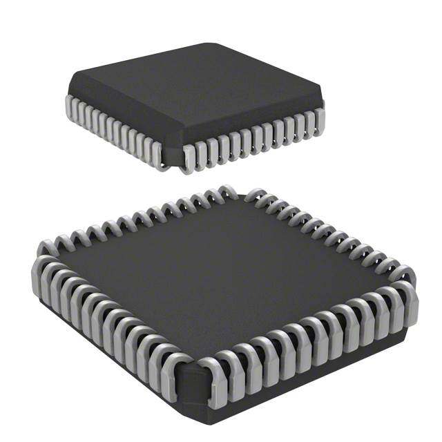
| 描述 | IC UART FIFO 16BYTE 32QFNUART 接口集成电路 UART |
| 产品分类 | |
| FIFO | 16 字节 |
| 品牌 | Exar Corporation |
| 产品手册 | |
| 产品图片 |
|
| rohs | 符合RoHS无铅 / 符合限制有害物质指令(RoHS)规范要求 |
| 产品系列 | 接口 IC,UART 接口集成电路,Exar XR16L580IL-F- |
| 数据手册 | http://www.exar.com/Common/Content/Document.ashx?id=277 |
| 产品型号 | XR16L580IL-F |
| PCN其它 | |
| 产品种类 | UART 接口集成电路 |
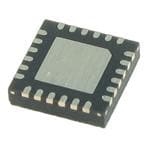
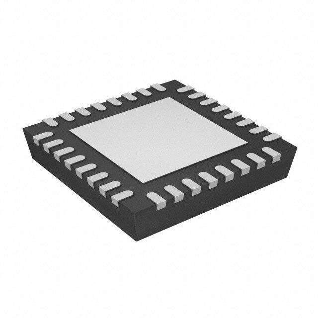
| 供应商器件封装 | 32-QFN(5x5) |
| 其它名称 | 1016-1423 |
| 包装 | 托盘 |
| 协议 | RS232,RS422 |
| 商标 | Exar |
| 安装类型 | 表面贴装 |
| 安装风格 | SMD/SMT |
| 封装/外壳 | 32-VFQFN 裸露焊盘 |
| 封装/箱体 | QFN-24 |
| 工厂包装数量 | 490 |
| 带CMOS | 是 |
| 带IrDA编码器/解码器 | 是 |
| 带假起始位检测 | 是 |
| 带并行端口 | - |
| 带自动流量控制 | 是 |
| 带调制解调器控制 | 是 |
| 数据速率 | 1 Mbps |
| 最大工作温度 | + 85 C |
| 最小工作温度 | - 40 C |
| 标准包装 | 490 |
| 特性 | - |
| 电压-电源 | 2.25 V ~ 5.5 V |
| 电源电压-最大 | 5.5 V |
| 电源电压-最小 | 2.25 V |
| 电源电流 | 3 mA |
| 通道数 | 1,UART |


- 商务部:美国ITC正式对集成电路等产品启动337调查
- 曝三星4nm工艺存在良率问题 高通将骁龙8 Gen1或转产台积电
- 太阳诱电将投资9.5亿元在常州建新厂生产MLCC 预计2023年完工
- 英特尔发布欧洲新工厂建设计划 深化IDM 2.0 战略
- 台积电先进制程称霸业界 有大客户加持明年业绩稳了
- 达到5530亿美元!SIA预计今年全球半导体销售额将创下新高
- 英特尔拟将自动驾驶子公司Mobileye上市 估值或超500亿美元
- 三星加码芯片和SET,合并消费电子和移动部门,撤换高东真等 CEO
- 三星电子宣布重大人事变动 还合并消费电子和移动部门
- 海关总署:前11个月进口集成电路产品价值2.52万亿元 增长14.8%


PDF Datasheet 数据手册内容提取
XR16L580 SMALLEST 2.25V TO 5.5V UART WITH 16-BYTE FIFO AND POWERSAVE AUGUST 2011 REV. 1.4.2 GENERAL DESCRIPTION FEATURES The XR16L580 (L580) is a 2.25 to 5.5 volt Universal • Smallest Full Featured UART Asynchronous Receiver and Transmitter (UART) with 5 volt • 2.25V to 5.5V Supply Voltage tolerant inputs and a reduced pin count. It is pin-to-pin and • 5V Tolerant Inputs (except XTAL1) software compatible to industry standard 16C450, 16C550, ST16C580, ST16C650A and XR16C850 UARTs. It has 16 • Intel/Motorola Bus Select bytes of TX and RX FIFOs and is capable of operating up to • ’0 ns’ Address Hold Time (T and T ) AH ADH serial data rate of 1 Mbps at 2.25 volt supply voltage. The • Pin and Software Compatible to industry standard internal registers is compatible to the 16C550 register set plus enhanced registers for additional features to support 16C450, 16C550, ST16C580, ST16C650A and today’s high bandwidth data communication needs. The XR16C850 in the 48-TQFP package. enhanced features include Intel or Motorola data bus • 16-byte Transmit FIFO interface to match your CPU interface, automatic hardware • 16-byte Receive FIFO with Errors Flags and software flow control to prevent data loss, selectable RX and TX trigger levels for more efficient interrupt service, • Selectable RX and TX FIFO Trigger Levels wireless infrared (IrDA) encoder/decoder for wireless • Automatic Hardware (RTS/CTS) Flow Control applications and a unique Power-Save mode to increase • Automatic Software (Xon/Xoff) Flow Control battery operating time. The device comes in the 48-TQFP and very small 32-QFN and 24-QFN packages in industrial • Up to 3.125 Mbps Data Rate at 5V and 2 Mbps at 3.3V temperature range. and 1 Mbps at 2.25V Operation with External Clock Input • Infrared (IrDA) Encoder/Decoder APPLICATIONS • Complete Modem Interface • Handheld Terminals and Tablets • Power-Save Mode to conserve battery power • Handheld Computers • Sleep Mode with Wake-up Interrupt • Wireless Portable Point-of-Sale Terminals • Small packages: 24-QFN (4x4x0.9mm) and 32-QFN • Cellular Phones DataPort (5x5x0.9mm) • GPS Devices • Compatible to standard 48-TQFP packages, without the • Personal Digital Assistants Modules following signals: IOR, IOW, CS1, CS2, TXRDY#, • Battery Operated Instruments RXRDY#, RCLK, BAUDOUT#, OP1# and OP2# • Industrial Temperature Grade(-40 to +85oC) FIGURE 1. BLOCK DIAGRAM *5 V Tolerant Inputs VCC PwrSave (Except for XTAL1) (2.25 to 5.5 V) A2:A0 GND D7:D0 UART IOR# TX, RX, IOW# (R/W#) 16 Byte TX FIFO UART RTS#, CTS#, CS# Regs DTR#, DSR#, IR TX & RX INT (IRQ#) ENDEC RI#, CD# Intel or Motorola RESET BRG 16 Byte RX FIFO (RESET#) Data Bus Interface 16/68# XTAL1 Crystal Osc/Buffer XTAL2 GNugget_BLK Exar Corporation 48720 Kato Road, Fremont CA, 94538 • (510) 668-7000 • FAX (510) 668-7017 • www.exar.com
XR16L580 SMALLEST 2.25V TO 5.5V UART WITH 16-BYTE FIFO AND POWERSAVE REV. 1.4.2 FIGURE 2. PACKAGES AND PIN OUT (24, 32-PIN QFN AND 48-TQFP PACKAGES) # et # et # Res INT A0 A1 A2 IOR Res IRQ A0 A1 A2 NC 18 17 16 15 14 13 18 17 16 15 14 13 VCC 19 12 GND VCC 19 12 GND D0 20 11 IOW# D0 20 11 R/W# 24-pin QFN in D1 21 24-pin QFN in 10 XTAL2 D1 21 10 XTAL2 Motorola Bus D2 22 Intel Bus mode 9 XTAL1 D2 22 mode 9 XTAL1 D3 23 8 PwrSv D3 23 8 PwrSv D4 24 7 CS# D4 24 7 CS# 1 2 3 4 5 6 1 2 3 4 5 6 # 5 6 7 X X # 5 6 7 X X 68 D D D R T 68 D D D R T 6/ 6/ 1 1 VCC GND # T T CTS#RESEDTR#RTS#INTA0A1A2 CTS#RESEDTR#RTS#IRQ#A0A1A2 2423222120191817 2423222120191817 DSR#25 16 NC DSR# 25 16 NC CD# 26 15 NC CD# 26 15 NC RI# 27 14IOR# RI# 27 32-pin QFN in 14 NC VCC 28 32-pin QFN in 13GND VCC 28 Motorola Bus 13 GND D0 29 Intel Bus Mode 12IOW# D0 29 Mode 12 R/W# D1 30 11XTAL2 D1 30 11 XTAL2 D2 31 10XTAL1 D2 31 10 XTAL1 D3 32 9 PwrSave D3 32 9 PwrSave 1 2 3 4 5 6 7 8 1 2 3 4 5 6 7 8 D4 6/68#D5D6D7RXTXCS# D416/68#D5D6D7RXTXCS# 1 VCC GND # T T NCRESENCDTR#RTS#NCINTNCA0A1A2NC NCRESENCDTR#RTS#NCIRQ#NCA0A1A2NC NC 3736 35 34 33 32 31 30 29 28 27 26 2524 NC NC 3736 35 34 33 32 31 30 29 28 27 26 2254 NC CTS# 38 23 NC CTS# 38 23 NC DSR# 39 22 NC DSR# 39 22 NC CD# 40 21 NC CD# 40 21 NC RI# 41 20 NC RI# 41 20 NC VCC 42 48-TQFP in 19 IOR# VCC 42 48-TQFP in 19 NC D0 43 18 GND D0 43 18 GND Intel Bus Mode Motorola Bus Mode D1 44 17 NC D1 44 17 NC D2 45 16 IOW# D2 45 16 R/W# D3 46 15 XTAL2 D3 46 15 XTAL2 D4 47 14 XTAL1 D4 47 14 XTAL1 NC 48 13 PwrSave NC 48 13 PwrSave 1 2 3 4 5 6 7 8 9 10 11 12 1 2 3 4 5 6 7 8 9 10 11 12 16/68#D5D6D7NCNCRXTXNCNCCS#NC 16/68#D5D6D7NCNCRXTXNCNCCS#NC VCC GND 2
XR16L580 REV. 1.4.2 SMALLEST 2.25V TO 5.5V UART WITH 16-BYTE FIFO AND POWERSAVE ORDERING INFORMATION OPERATING TEMPERATURE PART NUMBER PACKAGE DEVICE STATUS RANGE XR16L580IL24-F 24-Lead QFN -40°C to +85°C Active XR16L580IL24TR-F 24-Lead QFN -40°C to +85°C Active XR16L580IL-F 32-Lead QFN -40°C to +85°C Active XR16L580ILTR-F 32-Lead QFN -40°C to +85°C Active XR16L580IM-F 48-Lead TQFP -40°C to +85°C Active XR16L580IMTR-F 48-Lead TQFP -40°C to +85°C Active NOTE: TR = Tape and Reel, F = Green / RoHS 3
XR16L580 SMALLEST 2.25V TO 5.5V UART WITH 16-BYTE FIFO AND POWERSAVE REV. 1.4.2 PIN DESCRIPTIONS Pin Descriptions 48- 24-QFN 32-QFN NAME TQFP TYPE DESCRIPTION PIN# PIN# PIN# DATA BUS INTERFACE A2 14 17 26 I Address data lines [2:0]. These 3 address lines select one of the internal A1 15 18 27 registers in UART channel A/B during a data bus transaction. A0 16 19 28 D7 4 5 4 I/O Data bus lines [7:0] (bidirectional). D6 3 4 3 D5 2 3 2 D4 24 1 47 D3 23 32 46 D2 22 31 45 D1 21 30 44 D0 20 29 43 IOR# 13 14 19 I When 16/68# pin is at logic 1, the Intel bus interface is selected and this (NC) input becomes read strobe (active low). The falling edge instigates an internal read cycle and retrieves the data byte from an internal register pointed by the address lines [A2:A0], puts the data byte on the data bus to allow the host processor to read it on the rising edge. When 16/68# pin is at logic 0, the Motorola bus interface is selected and this input is not used. IOW# 11 12 16 I When 16/68# pin is at logic 1, it selects Intel bus interface and this input (R/W#) becomes write strobe (active low). The falling edge instigates the internal write cycle and the rising edge transfers the data byte on the data bus to an internal register pointed by the address lines. When 16/68# pin is at logic 0, the Motorola bus interface is selected and this input becomes read (logic 1) and write (logic 0) signal. CS# 7 8 11 I This input is chip select (active low) to enable the device. INT 17 20 30 O When 16/68# pin is at logic 1 for Intel bus interface, this output become (IRQ#) (OD) the active high device interrupt output. The output state is defined by the user through the software setting of MCR[3]. INT is set to the active mode when MCR[3] is set to a logic 1. INT is set to the three state mode when MCR[3] is set to a logic 0. See MCR[3]. When 16/68# pin is at logic 0 for Motorola bus interface, this output becomes the active low device interrupt output (open drain). An external pull-up resistor is required for proper operation. MODEM OR SERIAL I/O INTERFACE TX 6 7 8 O UART Transmit Data or infrared encoder data. Standard transmit and receive interface is enabled when MCR[6] = 0. In this mode, the TX signal will be a logic 1 during reset or idle (no data). Infrared IrDA transmit and receive interface is enabled when MCR[6] = 1. In the Infrared mode, the inactive state (no data) for the Infrared encoder/decoder interface is a logic 0. If it is not used, leave it unconnected. RX 5 6 7 I UART Receive Data or infrared receive data. Normal receive data input must idle at logic 1 condition. The infrared receiver idles at logic 0. 4
XR16L580 REV. 1.4.2 SMALLEST 2.25V TO 5.5V UART WITH 16-BYTE FIFO AND POWERSAVE Pin Descriptions 48- 24-QFN 32-QFN NAME TQFP TYPE DESCRIPTION PIN# PIN# PIN# RTS# - 21 32 O UART Request-to-Send (active low) or general purpose output. This out- put must be asserted prior to using auto RTS flow control, see EFR[6], MCR[1] and IER[6]. This pin is not available in the 24-QFN package. CTS# - 24 38 I UART Clear-to-Send (active low) or general purpose input. It can be used for auto CTS flow control, see EFR[7], MSR[4] and IER[7]. This input should be connected to VCC when not used. This pin is not avail- able in the 24-QFN package. DTR# - 22 33 O UART Data-Terminal-Ready (active low) or general purpose output. This pin is not available in the 24-QFN package. DSR# - 25 39 I UART Data-Set-Ready (active low) or general purpose input. This input should be connected to VCC when not used. This input has no effect on the UART. This pin is not available in the 24-QFN package. CD# - 26 40 I UART Carrier-Detect (active low) or general purpose input. This input should be connected to VCC when not used. This input has no effect on the UART. This pin is not available in the 24-QFN package. RI# - 27 41 I UART Ring-Indicator (active low) or general purpose input. This input should be connected to VCC when not used. This input has no effect on the UART. This pin is not available in the 24-QFN package. ANCILLARY SIGNALS XTAL1 9 10 14 I Crystal or external clock input. This input is not 5V tolerant. XTAL2 10 11 15 O Crystal or buffered clock output. This output may be use to drive a clock buffer which can drive other device(s). PwrSave 8 9 13 I Power-Save (active high). This feature isolates the L580’s data bus inter- face from the host preventing other bus activities that cause higher power drain during sleep mode. See Sleep Mode with Auto Wake-up and Power-Save Feature section for details. This pin has an internal pull- down resistor in the 48-TQFP package. The 32-QFN package does not have this pull-down resistor. 16/68# 1 2 1 I Intel or Motorola Bus Select. This pin has an internal pull-up resistor in the 48-TQFP package. The 32-QFN package does not have this resistor. When 16/68# pin is at logic 1, 16 or Intel Mode, the device will operate in the Intel bus type of interface. When 16/68# pin is at logic 0, 68 or Motorola mode, the device will oper- ate in the Motorola bus type of interface. RESET 18 23 35 I When 16/68# pin is at logic 1 for Intel bus interface, this input becomes (RESET#) RESET (active high). When 16/68# pin is at logic 0 for Motorola bus inter- face, this input becomes RESET# (active low). A 40 ns minimum active pulse on this pin will reset the internal registers and all outputs of the UART. The UART transmitter output will be held at logic 1, the receiver input will be ignored and outputs are reset during reset period (see UART Reset Conditions). VCC 19 28 42 Pwr 2.25V to 5.5V power supply. All input pins, except XTAL1, are 5V tolerant. GND 12 13 18 Pwr Power supply common, ground. 5
XR16L580 SMALLEST 2.25V TO 5.5V UART WITH 16-BYTE FIFO AND POWERSAVE REV. 1.4.2 Pin Descriptions 48- 24-QFN 32-QFN NAME TQFP TYPE DESCRIPTION PIN# PIN# PIN# GND Center Center N/A Pwr The exposed pad at the bottom surface of the package is designed for Pad Pad thermal performance. Use of a center pad on the PCB is strongly recom- mended for thermal conductivity as well as to provide mechanical stability of the package on the PCB. The center pad is recommended to be solder masked defined with opening size less than or equal to the exposed ther- mal pad on the package bottom to prevent solder bridging to the outer leads of the device. Thermal vias must be connected to GND plane as the thermal pad of package is at GND potential. NC - 15, 16 5, 6, 9, No Connects. Note that in Motorola mode, the IOR# pin becomes an NC 10, 12, - pin. 17, 20- 25, 29, 31, 34, 36, 37, 48 NOTE: Pin type: I=Input, O=Output, I/O= Input/output, OD=Output Open Drain. 6
XR16L580 REV. 1.4.2 SMALLEST 2.25V TO 5.5V UART WITH 16-BYTE FIFO AND POWERSAVE 1.0 PRODUCT DESCRIPTION The XR16L580 (L580) is an enhanced 16C550 Universal Asynchronous Receiver and Transmitter (UART). Its features set is compatible to the ST16C580 device and additionally offers Intel or Motorola data bus interface and Power-Save to isolate the data bus interface during Sleep mode. Hence, the L580 adds 2 more inputs: 16/ 68# and PwrSave pins. The XR16L580 can operate from 2.25V to 5.5V with 5 volt tolerant inputs. The configuration registers set is 16550 UART compatible for control, status and data transfer. Also, the L580 has 16-bytes of transmit and receive FIFOs, automatic RTS/CTS hardware flow control, automatic Xon/Xoff and special character software flow control, transmit and receive FIFO trigger levels, infrared encoder and decoder (IrDA ver 1.0), programmable baud rate generator with a prescaler of divide by 1 or 4. The L580 is fabricated using an advanced CMOS process. Enhanced Features The L580 UART provides a solution that supports 16 bytes of transmit and receive FIFO memory. The L580 is designed to work with low supply voltage and high performance data communication systems, that require fast data processing time. Increased performance is realized in the L580 by the transmit and receive FIFOs, FIFO trigger level controls and automatic flow control mechanism. This allows the external processor to handle more networking tasks within a given time. This increases the service interval giving the external CPU additional time for other applications and reducing the overall UART interrupt servicing time. In addition, the L580 provides the Power-Save mode that drastically reduces the power consumption when the device is not used. The combination of the above greatly reduces the CPU’s bandwidth requirement, increases performance, and reduces power consumption. Data Bus Interface, Intel or Motorola Type The L580 provides a host interface that supports Intel or Motorola microprocessor (CPU) data bus interface. The Intel bus compatible interface allows direct interconnect to Intel compatible type of CPUs using IOR#, IOW# and CS# inputs for data bus operation. The Motorola bus compatible interface instead uses the R/W# and CS# signals for data bus transactions. See pin description section for details on all the control signals. The Intel and Motorola bus interface selection is made through the pin, 16/68#. Data Rate The L580 is capable of operation up to 3.125 Mbps at 5V, 2 Mbps at 3.3V and 1 Mbps at 2.5V supply with 16X internal sampling clock rate. The device can operate with an external 24 MHz crystal on pins XTAL1 and XTAL2, or external clock source of up to 50 MHz on XTAL1 pin. With a typical crystal of 14.7456 MHz, all standard data rates of up to 921.6 kbps can be generated. Internal Enhanced Register Sets The L580 UART has a set of enhanced registers providing control and monitoring functions. Interrupt enable/ disable and status, FIFO enable/disable, selectable TX and RX FIFO trigger levels, automatic hardware/ software flow control enable/disable, programmable baud rates, infrared encoder/decoder enable/disable, modem interface controls and status, sleep mode and Power-Save mode are all standard features. Following a power on reset or an external reset (and operating in 16 or Intel Mode), the registers defaults to the reset condition and its is compatible with previous generation of UARTs, 16C450, 16C550, 16C580, 16C650A and 16C850. 7
XR16L580 SMALLEST 2.25V TO 5.5V UART WITH 16-BYTE FIFO AND POWERSAVE REV. 1.4.2 2.0 FUNCTIONAL DESCRIPTIONS 2.1 CPU Interface The CPU interface is 8 data bits wide with 3 address lines and control signals to execute data bus read and write transactions. The L580 data interface supports the Intel compatible types of CPUs and it is compatible to the industry standard 16C550 UART. No clock (oscillator nor external clock) is required to operate a data bus transaction. Each bus cycle is asynchronous using CS#, IOR# and IOW# or R/W# inputs. A typical data bus interconnection for Intel and Motorola mode is shown in Figure 3. FIGURE 3. XR16L580 TYPICAL INTEL/MOTOROLA DATA BUS INTERCONNECTIONS D0 D0 VCC VCC D1 D1 16/68# D2 D2 D3 D3 D4 D4 TX D5 D5 D6 D6 RX D7 D7 Serial Interface of RS-232 or RS-422 DTR# A0 A0 A1 A1 RTS# A2 A2 CTS# IOR# IOR# DSR# IOW# IOW# CD# UART_CS# CS# RI# UART_INT INT PwrSave GND UART_RESET RESET Intel Data Bus Interconnections D0 D0 VCC VCC D1 D1 D2 D2 PwrSave D3 D3 D4 D4 TX D5 D5 D6 D6 RX D7 D7 Serial Interface of RS-232 or RS-422 DTR# A0 A0 A1 A1 RTS# A2 A2 CTS# VCC IOR# DSR# R/W# IOW# CD# UART_CS# CS# RI# UART_IRQ# INT 16/68# GND UART_RESET# RESET Motorola Data Bus Interconnections 8
XR16L580 REV. 1.4.2 SMALLEST 2.25V TO 5.5V UART WITH 16-BYTE FIFO AND POWERSAVE 2.2 5-Volt Tolerant Inputs The L580 can accept up to 5V inputs when operating at 3.3V or 2.5V. But note that if the L580 is operating at 2.5V, its V may not be high enough to meet the requirements of the V of a CPU or a serial transceiver that OH IH is operating at 5V. Note that the XTAL1 pin is not 5V tolerant when external clock supply is used. 2.3 Device Hardware Reset The RESET or RESET# input resets the internal registers and the serial interface outputs in both channels to their default state (see Table 11). An active pulse of longer than 40 ns duration will be required to activate the reset function in the device. 2.4 Device Identification and Revision The XR16L580 provides a Device Identification code and a Device Revision code to distinguish the part from other devices and revisions. To read the identification code from the part, it is required to set the baud rate generator registers DLL and DLM both to 0x00. Now reading the content of the DLM will provide 0x01 to indicate XR16L580 and reading the content of DLL will provide the revision of the part; for example, a reading of 0x01 means revision A. 2.5 Internal Registers The L580 has a set of enhanced registers for control, monitoring and data loading and unloading. The configuration register set is compatible to those already available in the standard 16C550. These registers function as data holding registers (THR/RHR), interrupt status and control registers (ISR/IER), a FIFO control register (FCR), receive line status and control registers, (LSR/LCR), modem status and control registers (MSR/ MCR), programmable data rate (clock) divisor registers (DLL/DLM), and an user accessible Scratchpad register (SPR). Beyond the general 16C550 features and capabilities, the L580 offers enhanced feature registers (EFR, Xon1, Xoff 1, Xon1 and Xoff2) that provide automatic RTS and CTS hardware flow control and Xon/Xoff software flow control. All the register functions are discussed in full detail later in “Section 3.0, UART INTERNAL REGISTERS” on page 22. 2.6 DMA Mode The DMA Mode (a legacy term) refers to data block transfer operation. The DMA mode affects the state of the RXRDY# and TXRDY# output pins available in the original 16C550. These pins are not available in the XR16L580. The DMA Enable bit (FCR bit-3) does not have any function in this device and can be a ’0’ or a ’1’. 2.7 INT (IRQ#) Output The interrupt output changes according to the operating mode and enhanced features setup. Table 1 and Table 2 below summarize the operating behavior for the transmitter and receiver in the Intel and Motorola modes. Also see Figures 20 through 23. TABLE 1: INT (IRQ#) PIN OPERATION FOR TRANSMITTER FCR BIT-0 = 0 (FIFO DISABLED) FCR BIT-0 = 1 (FIFO ENABLED) INT Pin 0 = one byte in THR 0 = FIFO above trigger level (16/68# = 1) 1 = THR empty 1 = FIFO below trigger level or FIFO empty IRQ# Pin 1 = one byte in THR 1 = FIFO above trigger level (16/68# = 0) 0 = THR empty 0 = FIFO below trigger level or FIFO empty 9
XR16L580 SMALLEST 2.25V TO 5.5V UART WITH 16-BYTE FIFO AND POWERSAVE REV. 1.4.2 TABLE 2: INT (IRQ#) PIN OPERATION FOR RECEIVER FCR BIT-0 = 0 FCR BIT-0 = 1 (FIFO DISABLED) (FIFO ENABLED) INT Pin 0 = no data 0 = FIFO below trigger level (16/68# = 1) 1 = 1 byte 1 = FIFO above trigger level IRQ# Pin 1 = no data 1 = FIFO below trigger level (16/68# = 0) 0 = 1 byte 0 = FIFO above trigger level 2.8 Crystal or External Clock Input The L580 includes an on-chip oscillator (XTAL1 and XTAL2) to generate a clock when a crystal is connected between the XTAL1 and XTAL2 pins of the device. Alternatively, an external clock can be supplied through the XTAL1 pin. The CPU data bus does not require this clock for bus operation. The crystal oscillator provides a system clock to the Baud Rate Generators (BRG) section. XTAL1 is the input to the oscillator or external clock input and XTAL2 pin is the bufferred output which can be used as a clock signal for other devices in the system. Please note that the input XTAL1 is not 5V tolerant and therefore, the maximum voltage at the pin should be VCC when an external clock is supplied. For programming details, see “Programmable Baud Rate Generator.” FIGURE 4. TYPICAL CRYSTAL CONNECTIONS XTAL1 XTAL2 R1 0-120 (Optional) R2 500K - 1M 1.8432 MHz Y1 to 24 MHz C1 C2 22-47pF 22-47pF The on-chip oscillator is designed to use an industry standard microprocessor crystal (parallel resonant, fundamental frequency with 10-22 pF capacitance load, ESR of 20-120 ohms and 100ppm frequency tolerance) connected externally between the XTAL1 and XTAL2 pins (see Figure 5). When VCC = 5V, the on- chip oscillator can operate with a crystal whose frequency is not greater than 24 MHz. On the other hand, the L580 can accept an external clock of up to 50MHz at XTAL1 pin, with a 2K ohms pull-up resistor on XTAL2 pin (as shown in Figure 5). This translates to a maximum of 3.125Mbps serial data rate at 5V. 10
XR16L580 REV. 1.4.2 SMALLEST 2.25V TO 5.5V UART WITH 16-BYTE FIFO AND POWERSAVE FIGURE 5. EXTERNAL CLOCK CONNECTION FOR EXTENDED DATA RATE External Clock vcc XTAL1 gnd VCC R1 2K XTAL2 For further reading on the oscillator circuit please see the Application Note DAN108 on the EXAR web site at http://www.exar.com. 2.9 Programmable Baud Rate Generator The L580 UART has its own Baud Rate Generator (BRG) with a prescaler. The prescaler is controlled by a software bit (bit-7) in the MCR register. This bit selects the prescaler to divide the input crystal or external clock by a factor of 1 or 4. The clock output of the prescaler goes to the BRG. The BRG further divides this clock by a programmable divisor (via DLL and DLM registers) between 1 and (216 -1) to obtain a 16X sampling rate clock of the serial data rate. The sampling rate clock is used by the transmitter for data bit shifting and receiver for data sampling. The BRG divisor defaults to the maximum baud rate (DLL = 0x01 and DLM = 0x00) upon power up. FIGURE 6. BAUD RATE GENERATOR AND PRESCALER DLL and DLM Registers Prescaler MCR Bit-7=0 Divide by 1 (default) 16X XTAL1 Crystal Baud Rate Sampling XTAL2 Osc/ Generator Rate Clock to Buffer Logic Transmitter Prescaler Divide by 4 MCR Bit-7=1 Programming the Baud Rate Generator Registers DLM and DLL provides the capability of selecting the operating data rate. Table 3 shows the standard data rates available with a 14.7456 MHz crystal or external clock at 16X sampling rate clock rate. When using a non-standard data rate crystal or external clock, the divisor value can be calculated for DLL/DLM with the following equation. divisor (decimal) = (XTAL1 clock frequency / prescaler) / (serial data rate x 16) 11
XR16L580 SMALLEST 2.25V TO 5.5V UART WITH 16-BYTE FIFO AND POWERSAVE REV. 1.4.2 TABLE 3: TYPICAL DATA RATES WITH A 14.7456 MHZ CRYSTAL OR EXTERNAL CLOCK OUTPUT Data Rate OUTPUT Data Rate DLM DLL DIVISOR FOR 16x DIVISOR FOR 16x DATA RATE MCR Bit-7=1 MCR Bit-7=0 PROGRAM PROGRAM Clock (Decimal) Clock (HEX) ERROR (%) (DEFAULT) VALUE (HEX) VALUE (HEX) 100 400 2304 900 09 00 0 600 2400 384 180 01 80 0 1200 4800 192 C0 00 C0 0 2400 9600 96 60 00 60 0 4800 19.2k 48 30 00 30 0 9600 38.4k 24 18 00 18 0 19.2k 76.8k 12 0C 00 0C 0 38.4k 153.6k 6 06 00 06 0 57.6k 230.4k 4 04 00 04 0 115.2k 460.8k 2 02 00 02 0 230.4k 921.6k 1 01 00 01 0 12
XR16L580 REV. 1.4.2 SMALLEST 2.25V TO 5.5V UART WITH 16-BYTE FIFO AND POWERSAVE 2.10 Transmitter The transmitter section comprises of an 8-bit Transmit Shift Register (TSR) and 16 bytes of FIFO which includes a byte-wide Transmit Holding Register (THR). TSR shifts out every data bit with the 16X internal clock. A bit time is 16 clock periods. The transmitter sends the start-bit followed by the number of data bits, inserts the proper parity-bit if enabled, and adds the stop-bit(s). The status of the FIFO and TSR are reported in the Line Status Register (LSR bit-5 and bit-6). 2.10.1 Transmit Holding Register (THR) - Write Only The transmit holding register is an 8-bit register providing a data interface to the host processor. The host writes transmit data byte to the THR to be converted into a serial data stream including start-bit, data bits, parity-bit and stop-bit(s). The least-significant-bit (Bit-0) becomes first data bit to go out. The THR is the input register to the transmit FIFO of 16 bytes when FIFO operation is enabled by FCR bit-0. Every time a write operation is made to the THR, the FIFO data pointer is automatically bumped to the next sequential data location. 2.10.2 Transmitter Operation in non-FIFO Mode The host loads transmit data to THR one character at a time. The THR empty flag (LSR bit-5) is set when the data byte is transferred to TSR. THR flag can generate a transmit empty interrupt (ISR bit-1) when it is enabled by IER bit-1. The TSR flag (LSR bit-6) is set when TSR becomes completely empty. FIGURE 7. TRANSMITTER OPERATION IN NON-FIFO MODE Data Transmit Byte Holding Register (THR) THR Interrupt (ISR bit-1) Enabled by IER bit-1 16X Clock M L Transmit Shift Register (TSR) S S B B TXNOFIFO1 2.10.3 Transmitter Operation in FIFO Mode The host may fill the transmit FIFO with up to 16 bytes of transmit data. The THR empty flag (LSR bit-5) is set whenever the FIFO is empty. The THR empty flag can generate a transmit empty interrupt (ISR bit-1) when the amount of data in the FIFO falls below its programmed trigger level. The transmit empty interrupt is enabled by IER bit-1. The Transmitter Empty Flag (LSR bit-6) is set when both the TSR and the FIFO become empty. 13
XR16L580 SMALLEST 2.25V TO 5.5V UART WITH 16-BYTE FIFO AND POWERSAVE REV. 1.4.2 FIGURE 8. TRANSMITTER OPERATION IN FIFO AND FLOW CONTROL MODE THR Interrupt (ISR bit-1): Transmit Transmit Data Byte FIFO - When the TX FIFO falls below the programmed Trigger Level, and - When the TX FIFO becomes empty. Auto CTS Flow Control (CTS# pin) FIFO is Enabled by FCR bit-0=1 Flow Control Characters (Xoff1,2 and Xon1,2 Reg.) Auto Software Flow Control 16X Clock Transmit Data Shift Register (TSR) TXFIFO1 2.11 RECEIVER The receiver section contains an 8-bit Receive Shift Register (RSR) and 16 bytes of FIFO which includes a byte-wide Receive Holding Register (RHR). The RSR uses the 16X clock for timing. On the falling edge of a start or a false start bit, an internal receiver counter starts counting at the 16X clock rate. After 8 clocks the start bit period should be at the center of the start bit. At this time the start bit is sampled and if it is still a logic 0 it is validated as a start bit. Evaluating the start bit in this manner prevents the receiver from assembling a false character. Each of the data, parity and stop bits is sampled at the middle of the bit to prevent false framing. If there were any error(s), they are reported in the LSR register bits 2-4. Upon unloading the receive data byte from RHR, the receive FIFO pointer is bumped and the error tags are immediately updated to reflect the status of the data byte in RHR register. RHR can generate a receive data ready interrupt upon receiving a character or delay until it reaches the FIFO trigger level. Furthermore, data delivery to the host is guaranteed by a receive data ready time-out interrupt when data is not received for 4 word lengths as defined by LCR[1:0] plus 12 bits time. This is equivalent to 3.7-4.6 character times. The RHR interrupt is enabled by IER bit-0. 2.11.1 Receive Holding Register (RHR) - Read-Only The Receive Holding Register is an 8-bit register that holds a receive data byte from the Receive Shift Register. It provides the receive data interface to the host processor. The RHR register is part of the receive FIFO of 16 bytes by 11-bits wide, the 3 extra bits are for the 3 error tags to be reported in LSR register. When the FIFO is enabled by FCR bit-0, the RHR contains the first data character received by the FIFO. After the RHR is read, the next character byte is loaded into the RHR and the errors associated with the current data byte are immediately updated in the LSR bits 2-4. 14
XR16L580 REV. 1.4.2 SMALLEST 2.25V TO 5.5V UART WITH 16-BYTE FIFO AND POWERSAVE FIGURE 9. RECEIVER OPERATION IN NON-FIFO MODE 16X Clock Receive Data Shift Data Bit Register (RSR) Validation Receive Data Characters Error Receive Tags in Receive Data Data Byte LSR bits Holding Register RHR Interrupt (ISR bit-2) and Errors 4:2 (RHR) RXFIFO1 FIGURE 10. RECEIVER OPERATION IN FIFO AND AUTO RTS FLOW CONTROL MODE 16X Clock Receive Data Shift Data Bit Register (RSR) Validation Receive Data Characters Example : RX FIFO trigger level selected at 8 bytes 16 bytes by 11-bit wide FIFO Data falls to RTS# re-asserts when data falls below the flow 4 control trigger level to restart remote transmitter. Enable by EFR bit-6=1, MCR bit-1. gss) Receive Error Ta(16-set Data FIFO FIFO Trigger=8 RdFeIHFsROir e Iidns t FeErInrFuaOpb tlet r(diIgS bgRye rbF liCet-v2Re) lbp.irto-0g=ra1mmed for Data fills to RTS# de-asserts when data fills above the flow 14 control trigger level to suspend remote transmitter. RByetcee aivned D Eartraors or Tags inR bits 4:2 ReDcaetiave Enable by EFR bit-6=1, MCR bit-1. ErrLS RXFIFO1 15
XR16L580 SMALLEST 2.25V TO 5.5V UART WITH 16-BYTE FIFO AND POWERSAVE REV. 1.4.2 2.12 Auto RTS (Hardware) Flow Control This feature is not available in the 24-QFN package since it does not have the RTS# pin. Automatic RTS hardware flow control is used to prevent data overrun to the local receiver FIFO. The RTS# output is used to request remote unit to suspend/resume data transmission. The auto RTS flow control features is enabled to fit specific application requirement (see Figure 11): • Enable auto RTS flow control using EFR bit-6. • The auto RTS function must be started by asserting RTS# output pin (MCR bit-1 to logic 1 after it is enabled). If using the Auto RTS interrupt: • Enable RTS interrupt through IER bit-6 (after setting EFR bit-4). The UART issues an interrupt when the RTS# pin makes a transition from low to high: ISR bit-5 will be set to logic 1. 2.13 Auto RTS Hysteresis The L580 has a new feature that provides flow control trigger hysteresis while maintaining compatibility with the ST16C550 UART. With the Auto RTS function enabled, an interrupt is generated when the receive FIFO reaches the programmed RX trigger level. The RTS# pin will not be forced to a logic 1 (RTS off), until the receive FIFO reaches one trigger level above the programmed trigger level in the trigger table (Table 8). The RTS# pin will return to a logic 0 after the RX FIFO is unloaded to one trigger level lower than the programmed trigger level. This is described in Figure 11. Under the above described conditions, the L580 will continue to accept data until the receive FIFO gets full. The Auto RTS function is initiated when the RTS# output pin is asserted to a logic 0 (RTS On). 2.14 Auto CTS Flow Control This feature is not available in the 24-QFN package since it does not have the CTS# pin. Automatic CTS flow control is used to prevent data overrun to the remote receiver FIFO. The CTS# input is monitored to suspend/restart the local transmitter. The auto CTS flow control feature is selected to fit specific application requirement (see Figure 11): • Enable auto CTS flow control using EFR bit-7. If using the Auto CTS interrupt: • Enable CTS interrupt through IER bit-7 (after setting EFR bit-4). The UART issues an interrupt when the CTS# pin is de-asserted (HIGH): ISR bit-5 will be set to 1, and UART will suspend transmission as soon as the stop bit of the character in process is shifted out. Transmission is resumed after the CTS# input is re- asserted (LOW), indicating more data may be sent. 16
XR16L580 REV. 1.4.2 SMALLEST 2.25V TO 5.5V UART WITH 16-BYTE FIFO AND POWERSAVE FIGURE 11. AUTO RTS AND CTS FLOW CONTROL OPERATION (NOT AVAILABLE IN 24-QFN PACKAGE) Local UART Remote UART UARTA UARTB Receiver FIFO RXA TXB Transmitter Trigger Reached Auto RTS RTSA# CTSB# Auto CTS Trigger Level Monitor TXA RXB Receiver FIFO Transmitter Trigger Reached Auto CTS CTSA# RTSB# Auto RTS Monitor Trigger Level Assert RTS# to Begin Transmission 1 RTSA# ON OFF 10 ON 2 7 CTSB# ON 8 OFF 11 ON 3 TXB Restart Data Starts 6 Suspend 4 9 RXA FIFO INTA RDecaetaiveTrRigXg eFrI FLOevel 5 TRhTrSe sHhioglhd TRhTrSe sLhoowld 12 TRrXig gFeIFr OLevel (RXA FIFO Interrupt) RTSCTS1 The local UART (UARTA) starts data transfer by asserting RTSA# (1). RTSA# is normally connected to CTSB# (2) of remote UART (UARTB). CTSB# allows its transmitter to send data (3). TXB data arrives and fills UARTA receive FIFO (4). When RXA data fills up to its receive FIFO trigger level, UARTA activates its RXA data ready interrupt (5) and con- tinues to receive and put data into its FIFO. If interrupt service latency is long and data is not being unloaded, UARTA monitors its receive data fill level to match the upper threshold of RTS delay and de-assert RTSA# (6). CTSB# follows (7) and request UARTB transmitter to suspend data transfer. UARTB stops or finishes sending the data bits in its trans- mit shift register (8). When receive FIFO data in UARTA is unloaded to match the lower threshold of RTS delay (9), UARTA re-asserts RTSA# (10), CTSB# recognizes the change (11) and restarts its transmitter and data flow again until next receive FIFO trigger (12). This same event applies to the reverse direction when UARTA sends data to UARTB with RTSB# and CTSA# controlling the data flow. 17
XR16L580 SMALLEST 2.25V TO 5.5V UART WITH 16-BYTE FIFO AND POWERSAVE REV. 1.4.2 2.15 Auto Xon/Xoff (Software) Flow Control When software flow control is enabled (See Table 10), the L580 compares one or two sequential receive data characters with the programmed Xon or Xoff-1,2 character value(s). If receive character(s) (RX) match the programmed values, the L580 will halt transmission (TX) as soon as the current character has completed transmission. When a match occurs, the Xoff (if enabled via IER bit-5) flag will be set and the interrupt output pin will be activated. Following a suspension due to a match of the Xoff character, the L580 will monitor the receive data stream for a match to the Xon-1,2 character. If a match is found, the L580 will resume operation and clear the flags (ISR bit-4). Reset initially sets the contents of the Xon/Xoff 8-bit flow control registers to a logic 0. Following reset the user can write any Xon/Xoff value desired for software flow control. Different conditions can be set to detect Xon/ Xoff characters (See Table 10) and suspend/resume transmissions. When double 8-bit Xon/Xoff characters are selected, the L580 compares two consecutive receive characters with two software flow control 8-bit values (Xon1, Xon2, Xoff1, Xoff2) and controls TX transmissions accordingly. Under the above described flow control mechanisms, flow control characters are not placed (stacked) in the user accessible RX data buffer or FIFO. In the event that the receive buffer is overfilling and flow control needs to be executed, the L580 automatically sends an Xoff message (when enabled) via the serial TX output to the remote modem. The L580 sends the Xoff character(s) two-character-times (= time taken to send two characters at the programmed baud rate) after the receive FIFO crosses the programmed trigger level. To clear this condition, the L580 will transmit the programmed Xon character(s) as soon as receive FIFO is less than one trigger level below the programmed trigger level (see Table 8). The table below describes this. TABLE 4: AUTO XON/XOFF (SOFTWARE) FLOW CONTROL XOFF CHARACTER(S) SENT XON CHARACTER(S) SENT RX TRIGGER LEVEL INT PIN ACTIVATION (CHARACTERS IN RX FIFO) (CHARACTERS IN RX FIFO) 1 1 1* 0 4 4 4* 1 8 8 8* 4 14 14 14* 8 * After the trigger level is reached, an xoff character is sent after a short span of time (= time required to send 2 characters); for example, after 2.083ms has elapsed for 9600 baud and 8-bit word length, no parity and 1 stop bit setting. 2.16 Special Character Detect A special character detect feature is provided to detect an 8-bit character when bit-5 is set in the Enhanced Feature Register (EFR). When this character (Xoff2) is detected, it will be placed in the FIFO along with normal incoming RX data. The L580 compares each incoming receive character with the programmed Xoff-2 data. If a match exists, the received data will be transferred to the RX FIFO and ISR bit-4 will be set to indicate detection of special character. Although the Internal Register Table shows Xon, Xoff Registers with eight bits of character information, the actual number of bits is dependent on the programmed word length. Line Control Register (LCR) bits 0-1 defines the number of character bits, i.e., either 5 bits, 6 bits, 7 bits, or 8 bits. The word length selected by LCR bits 0-1 also determines the number of bits that will be used for the special character comparison. Bit-0 in the Xon, Xoff Registers corresponds with the LSB bit for the receive character. 18
XR16L580 REV. 1.4.2 SMALLEST 2.25V TO 5.5V UART WITH 16-BYTE FIFO AND POWERSAVE 2.17 Infrared Mode The L580 UART includes the infrared encoder and decoder compatible to the IrDA (Infrared Data Association) version 1.0. The IrDA 1.0 standard that stipulates the infrared encoder sends out a 3/16 of a bit wide HIGH- pulse for each “0” bit in the transmit data stream. This signal encoding reduces the on-time of the infrared LED, hence reduces the power consumption. See Figure 12 below. The infrared encoder and decoder are enabled by setting MCR register bit-6 to a ‘1’. When the infrared feature is enabled, the transmit data output, TX, idles at logic zero level. Likewise, the RX input assumes an idle level of logic zero from a reset and power up, see Figure 12. Typically, the wireless infrared decoder receives the input pulse from the infrared sensing diode on the RX pin. Each time it senses a light pulse, it returns a logic 1 to the data bit stream. However, this is not true with some infrared modules on the market which indicate a logic 0 by a light pulse. So the L580 has a provision to invert the input polarity to accommodate this. In this case, the user can enable MCR bit-2 to invert the IR signal at the RX pin. FIGURE 12. INFRARED TRANSMIT DATA ENCODING AND RECEIVE DATA DECODING Character art Data Bits op St St TX Data 0 1 0 1 0 0 1 1 0 1 Transmit IR Pulse (TX Pin) 1/2 Bit Time Bit Time 3/16 Bit Time IrEncoder-1 Receive IR Pulse (RX pin) Bit Time 1/16 Clock Delay RX Data 0 1 0 1 0 0 1 1 0 1 art Data Bits op St St Character IRdecoder- 19
XR16L580 SMALLEST 2.25V TO 5.5V UART WITH 16-BYTE FIFO AND POWERSAVE REV. 1.4.2 2.18 Sleep Mode with Wake-Up Interrupt and Power-Save Feature The L580 supports low voltage system designs, hence, a sleep mode with wake-up interrupt and Power-Save feature is included to reduce power consumption when the device is not actively used. 2.18.1 Sleep Mode All of these conditions must be satisfied for the L580 to enter sleep mode: ■ no interrupts pending (ISR bit-0 = 1) ■ the 16-bit divisor programmed in DLM and DLL registers is a non-zero value ■ sleep mode is enabled (IER bit-4 = 1) ■ modem inputs are not toggling (MSR bits 0-3 = 0) ■ RX input pin is idling at a logic 1 The L580 stops its crystal oscillator to conserve power in the sleep mode. User can check the XTAL2 pin for no clock output as an indication that the device has entered the sleep mode. The L580 resumes normal operation by any of the following: ■ a receive data start bit transition (logic 1 to 0) at the RX input pin ■ a data byte is loaded to the transmitter, THR or FIFO ■ a change of logic state on any of the modem or general purpose serial inputs: CTS#, DSR#, CD#, RI# If the L580 is awakened by any one of the above conditions, it issues an interrupt as soon as the oscillator circuit is up and running and the device is ready to transmit/receive. This interrupt has the same encoding (bit- 0 of ISR register = 1) as "no interrupt pending" and will clear when the ISR register is read. This will show up in the ISR register only if no other interrupts are enabled. The L580 will return to the sleep mode automatically after all interrupting conditions have been serviced and cleared. If the L580 is awakened by the modem inputs, a read to the MSR is required to reset the modem inputs. In any case, the sleep mode will not be entered while an interrupt is pending. The L580 will stay in the sleep mode of operation until it is disabled by setting IER bit-4 to a logic 0. 2.18.2 Power-Save Feature If the address lines, data bus lines, IOW#, IOR#, CS# and modem input lines remain steady when the L580 is in sleep mode, the maximum current will be in the microamp range as specified in the DC Electrical Characteristics on page 38. If the input lines are floating or are toggling while the L580 is in sleep mode, the current can be up to 100 times more. If not using the Power-Save feature, an external buffer would be required to keep the address and data bus lines from toggling or floating to achieve the low current. But if the Power- Save feature is enabled (PwrSave pin connected to VCC), this will eliminate the need for an external buffer by internally isolating the address, data and control signals (see Figure 1 on page 1) from other bus activities that could cause wasteful power drain. The L580 enters Power-Save mode when this pin is connected to VCC and the L580 is in sleep mode (see Sleep Mode section above). Since Power-Save mode isolates the address, data and control signals, the device will wake-up only by: ■ a receive data start bit transition (logic 1 to 0) at the RX input pin or ■ a change of logic state on any of the modem or general purpose serial inputs: CTS#, DSR#, CD# or RI# The L580 will return to the Power-Save mode automatically after a read to the MSR (to reset the modem inputs) and all interrupting conditions have been serviced and cleared. The L580 will stay in the Power-Save mode of operation until it is disabled by setting IER bit-4 to a logic 0 and/or the Power-Save pin is connected to GND. 20
XR16L580 REV. 1.4.2 SMALLEST 2.25V TO 5.5V UART WITH 16-BYTE FIFO AND POWERSAVE 2.19 Internal Loopback The L580 UART provides an internal loopback capability for system diagnostic purposes. The internal loopback mode is enabled by setting MCR register bit-4 to logic 1. All regular UART functions operate normally including automatic hardware and software flow control. Figure 13 shows how the modem port signals are re- configured. Transmit data from the transmit shift register output is internally routed to the receive shift register input allowing the system to receive the same data that it was sending. The TX pin is held at logic 1 or mark condition while RTS# and DTR# are de-asserted, and CTS#, DSR# CD# and RI# inputs are ignored. Caution: the RX input pins must be held to a logic 1 during loopback test else upon exiting the loopback test the UART may detect and report a false “break” signal. FIGURE 13. INTERNAL LOOP BACK VCC TX Transmit Shift Register (THR/FIFO) MCR bit-4=1 als Receive Shift Register n (RHR/FIFO) g RX Si VCC ol r t n RTS# o RTS# C d c n gi a o nes rol L CTS# CTS# s Li Cont VCC Bu e DTR# ata pos DTR# D ur ernal eral P DSR# DSR# Int Gen OP1# m / RI# RI# e d OP2# o M CD# CD# 21
XR16L580 SMALLEST 2.25V TO 5.5V UART WITH 16-BYTE FIFO AND POWERSAVE REV. 1.4.2 3.0 UART INTERNAL REGISTERS The L580 has a set of configuration registers selected by address lines A0, A1 and A2 with CS# asserted. The complete register set is shown on Table 5 and Table 6. TABLE 5: UART INTERNAL REGISTERS A2,A1,A0 ADDRESSES REGISTER READ/WRITE COMMENTS 16C550 COMPATIBLE REGISTERS 0 0 0 RHR - Receive Holding Register Read-only LCR[7] = 0 THR - Transmit Holding Register Write-only 0 0 0 DLL - Div Latch Low Byte Read/Write LCR[7] = 1 0 0 1 DLM - Div Latch High Byte Read/Write 0 0 0 DREV - Device Revision Code Read-only DLL, DLM = 0x00, 0 0 1 DVID - Device Identification Code Read-only LCR[7] = 1 0 0 1 IER - Interrupt Enable Register Read/Write LCR[7] = 0 0 1 0 ISR - Interrupt Status Register Read-only LCR ≠ 0xBF FCR - FIFO Control Register Write-only 0 1 1 LCR - Line Control Register Read/Write 1 0 0 MCR - Modem Control Register Read/Write 1 0 1 LSR - Line Status Register Read-only Reserved Write-only LCR ≠ 0xBF 1 1 0 MSR - Modem Status Register Read-only Reserved Write-only 1 1 1 SPR - Scratchpad Register Read/Write LCR ≠ 0xBF ENHANCED REGISTERS 0 1 0 EFR - Enhanced Function Register Read/Write 1 0 0 Xon-1 - Xon Character 1 Read/Write 1 0 1 Xon-2 - Xon Character 2 Read/Write LCR = 0xBF 1 1 0 Xoff-1 - Xoff Character 1 Read/Write 1 1 1 Xoff-2 - Xoff Character 2 Read/Write 22
XR16L580 REV. 1.4.2 SMALLEST 2.25V TO 5.5V UART WITH 16-BYTE FIFO AND POWERSAVE . TABLE 6: INTERNAL REGISTERS DESCRIPTION. SHADED BITS ARE ENABLED WHEN EFR BIT-4=1 ADDRESS REG READ/ BIT-7 BIT-6 BIT-5 BIT-4 BIT-3 BIT-2 BIT-1 BIT-0 COMMENT A2-A0 NAME WRITE 16C550 Compatible Registers 0 0 0 RHR RD Bit-7 Bit-6 Bit-5 Bit-4 Bit-3 Bit-2 Bit-1 Bit-0 0 0 0 THR WR Bit-7 Bit-6 Bit-5 Bit-4 Bit-3 Bit-2 Bit-1 Bit-0 0 0 1 IER RD/WR 0/ 0/ 0/ 0/ Modem RX Line TX RX Stat. Int. Stat. Empty Data LCR[7]=0 CTS Int. RTS Int. Xoff Int. Sleep Enable Int. Int Int. Enable Enable Enable Mode Enable Enable Enable Enable 0 1 0 ISR RD FIFOs FIFOs 0/ 0/ INT INT INT INT Enabled Enabled Source Source Source Source INT INT Bit-3 Bit-2 Bit-1 Bit-0 Source Source Bit-5 Bit-4 LCR ≠ 0xBF 0 1 0 FCR WR RX FIFO RX FIFO 0/ 0/ DMA TX RX FIFOs Trigger Trigger Mode FIFO FIFO Enable TX FIFO TX FIFO Enable Reset Reset Trigger Trigger 0 1 1 LCR RD/WR Divisor Set TX Set Par- Even Parity Stop Word Word Enable Break ity Parity Enable Bits Length Length Bit-1 Bit-0 1 0 0 MCR RD/WR 0/ 0/ 0/ Internal INT Out- (OP1#) RTS# DTR# Loop- put Output Output BRG IR Mode XonAny back Enable Invert Control Control Pres- ENable Enable (OP2#) IR RX caler 1 0 1 LSR RD RX FIFO THR & THR RX RX Fram- RX RX RX LCR ≠ 0xBF Global TSR Empty Break ing Error Parity Over- Data Error Empty Error run Ready Error 1 1 0 MSR RD CD# RI# DSR# CTS# Delta Delta Delta Delta Input Input Input Input CD# RI# DSR# CTS# 1 1 1 SPR RD/WR Bit-7 Bit-6 Bit-5 Bit-4 Bit-3 Bit-2 Bit-1 Bit-0 LCR ≠ 0xBF Baud Rate Generator Divisor 0 0 0 DLL RD/WR Bit-7 Bit-6 Bit-5 Bit-4 Bit-3 Bit-2 Bit-1 Bit-0 LCR[7]=1 0 0 1 DLM RD/WR Bit-7 Bit-6 Bit-5 Bit-4 Bit-3 Bit-2 Bit-1 Bit-0 0 0 0 DREV RD Bit-7 Bit-6 Bit-5 Bit-4 Bit-3 Bit-2 Bit-1 Bit-0 LCR[7]=1 DLL=0x00 0 0 1 DVID RD 0 0 0 0 0 0 0 1 DLM=0x00 23
XR16L580 SMALLEST 2.25V TO 5.5V UART WITH 16-BYTE FIFO AND POWERSAVE REV. 1.4.2 TABLE 6: INTERNAL REGISTERS DESCRIPTION. SHADED BITS ARE ENABLED WHEN EFR BIT-4=1 ADDRESS REG READ/ BIT-7 BIT-6 BIT-5 BIT-4 BIT-3 BIT-2 BIT-1 BIT-0 COMMENT A2-A0 NAME WRITE Enhanced Registers 0 1 0 EFR RD/WR Auto Auto Special Enable Soft- Soft- Soft- Soft- CTS RTS Char IER [7:4], ware ware ware ware Enable Enable Select ISR [5:4], Flow Flow Flow Flow FCR[5:4], Cntl Cntl Cntl Cntl MCR[7:5], Bit-2 Bit-1 Bit-0 MCR[2] Bit-3 LCR=0XBF 1 0 0 XON1 WR Bit-7 Bit-6 Bit-5 Bit-4 Bit-3 Bit-2 Bit-1 Bit-0 1 0 1 XON2 WR Bit-7 Bit-6 Bit-5 Bit-4 Bit-3 Bit-2 Bit-1 Bit-0 1 1 0 XOFF1 WR Bit-7 Bit-6 Bit-5 Bit-4 Bit-3 Bit-2 Bit-1 Bit-0 1 1 1 XOFF2 WR Bit-7 Bit-6 Bit-5 Bit-4 Bit-3 Bit-2 Bit-1 Bit-0 4.0 INTERNAL REGISTER DESCRIPTIONS 4.1 Receive Holding Register (RHR) - Read- Only SEE”RECEIVER” ON PAGE 14. 4.2 Transmit Holding Register (THR) - Write-Only SEE”TRANSMITTER” ON PAGE 13. 4.3 Baud Rate Generator Divisors (DLL and DLM) - Read/Write The Baud Rate Generator (BRG) is a 16-bit counter that generates the data rate for the transmitter. The rate is programmed through registers DLL and DLM which are only accessible when LCR bit-7 is set to ‘1’. SEE”PROGRAMMABLE BAUD RATE GENERATOR” ON PAGE 11. 4.4 Interrupt Enable Register (IER) - Read/Write The Interrupt Enable Register (IER) masks the interrupts from receive data ready, transmit empty, line status and modem status registers. These interrupts are reported in the Interrupt Status Register (ISR). 4.4.1 IER versus Receive FIFO Interrupt Mode Operation When the receive FIFO (FCR BIT-0 = 1) and receive interrupts (IER BIT-0 = 1) are enabled, the RHR interrupts (see ISR bits 2 and 3) status will reflect the following: A. The receive data available interrupts are issued to the host when the FIFO has reached the programmed trigger level. It will be cleared when the FIFO drops below the programmed trigger level. B. FIFO level will be reflected in the ISR register when the FIFO trigger level is reached. Both the ISR register status bit and the interrupt will be cleared when the FIFO drops below the trigger level. C. The receive data ready bit (LSR BIT-0) is set as soon as a character is transferred from the shift register to the receive FIFO. It is reset when the FIFO is empty. 24
XR16L580 REV. 1.4.2 SMALLEST 2.25V TO 5.5V UART WITH 16-BYTE FIFO AND POWERSAVE 4.4.2 IER versus Receive/Transmit FIFO Polled Mode Operation When FCR bit-0 equals a logic 1 for FIFO enable; resetting IER bits 0-3 enables the XR16L580 in the FIFO polled mode of operation. Since the receiver and transmitter have separate bits in the LSR either or both can be used in the polled mode by selecting respective transmit or receive control bit(s). A. LSR BIT-0 indicates there is data in RHR or RX FIFO. B. LSR BIT-1 indicates an overrun error has occurred and that data in the FIFO may not be valid. C. LSR BIT 2-4 provides the type of receive data errors encountered for the data byte in RHR, if any. D. LSR BIT-5 indicates THR is empty. E. LSR BIT-6 indicates when both the transmit FIFO and TSR are empty. F. LSR BIT-7 indicates a data error in at least one character in the RX FIFO. IER[0]: RHR Interrupt Enable The receive data ready interrupt will be issued when RHR has a data character in the non-FIFO mode or when the receive FIFO has reached the programmed trigger level in the FIFO mode. • Logic 0 = Disable the receive data ready interrupt (default). • Logic 1 = Enable the receiver data ready interrupt. IER[1]: THR Interrupt Enable This bit enables the Transmit Ready interrupt which is issued whenever the THR becomes empty in the non- FIFO mode or when data in the FIFO falls below the programmed trigger level in the FIFO mode. If the THR is empty when this bit is enabled, an interrupt will be generated. • Logic 0 = Disable Transmit Ready interrupt (default). • Logic 1 = Enable Transmit Ready interrupt. IER[2]: Receive Line Status Interrupt Enable If any of the LSR register bits 1, 2, 3 or 4 is a logic 1, it will generate an interrupt to inform the host controller about the error status of the current data byte in FIFO. LSR bit-1 generates an interrupt immediately when the character has been received. LSR bits 2-4 generate an interrupt when the character with errors is read out of the FIFO. • Logic 0 = Disable the receiver line status interrupt (default). • Logic 1 = Enable the receiver line status interrupt. IER[3]: Modem Status Interrupt Enable • Logic 0 = Disable the modem status register interrupt (default). • Logic 1 = Enable the modem status register interrupt. IER[4]: Sleep Mode Enable (requires EFR bit-4 = 1) • Logic 0 = Disable Sleep Mode (default). • Logic 1 = Enable Sleep Mode. See Sleep Mode section for further details. IER[5]: Xoff Interrupt Enable (requires EFR bit-4=1) • Logic 0 = Disable the software flow control, receive Xoff interrupt. (default) • Logic 1 = Enable the software flow control, receive Xoff interrupt. See Software Flow Control section for details. 25
XR16L580 SMALLEST 2.25V TO 5.5V UART WITH 16-BYTE FIFO AND POWERSAVE REV. 1.4.2 IER[6]: RTS# Output Interrupt Enable (requires EFR bit-4=1) This bit has no functionality in the 24-QFN package. • Logic 0 = Disable the RTS# interrupt (default). • Logic 1 = Enable the RTS# interrupt. The UART issues an interrupt when the RTS# pin makes a transition from low to high. IER[7]: CTS# Input Interrupt Enable (requires EFR bit-4=1) This bit has no functionality in the 24-QFN package. • Logic 0 = Disable the CTS# interrupt (default). • Logic 1 = Enable the CTS# interrupt. The UART issues an interrupt when CTS# pin makes a transition from low to high. 4.5 Interrupt Status Register (ISR) - Read-Only The UART provides multiple levels of prioritized interrupts to minimize external software interaction. The Interrupt Status Register (ISR) provides the user with six interrupt status bits. Performing a read cycle on the ISR will give the user the current highest pending interrupt level to be serviced, others are queued up to be serviced next. No other interrupts are acknowledged until the pending interrupt is serviced. The Interrupt Source Table, Table 7, shows the data values (bit 0-5) for the interrupt priority levels and the interrupt sources associated with each of these interrupt levels. 4.5.1 Interrupt Generation: • LSR is by any of the LSR bits 1, 2, 3 and 4. • RXRDY is by RX trigger level. • RXRDY Time-out is by a 4-char plus 12 bits delay timer. • TXRDY is by TX trigger level or TX FIFO empty. • MSR is by any of the MSR bits 0, 1, 2 and 3. • Receive Xoff/Special character is by detection of a Xoff or Special character. • CTS# is when its transmitter toggles the input pin (from low to high) during auto CTS flow control enabled by EFR bit-7. • RTS# is when its receiver toggles the output pin (from low to high) during auto RTS flow control enabled by EFR bit-6. • Wake-up Interrupt is when the device wakes up from sleep mode. See Sleep Mode section for more details. 4.5.2 Interrupt Clearing: • LSR interrupt is cleared by reading the LSR register (but FIFO error bit does not clear until the character(s) that generated the interrupt(s) is (are) read from the FIFO). • RXRDY interrupt is cleared by reading data until FIFO falls below the trigger level. • RXRDY Time-out interrupt is cleared by reading the RHR register. • TXRDY interrupt is cleared by reading the ISR register or writing to the THR register. • MSR interrupt is cleared by reading the MSR register. • Xoff interrupt is cleared by reading the ISR or when Xon character(s) is received. • Special character interrupt is cleared by reading the ISR or after the next character is received. • RTS# and CTS# flow control interrupts are cleared by reading the MSR register. • Wake-up interrupt is cleared by reading the ISR register. 26
XR16L580 REV. 1.4.2 SMALLEST 2.25V TO 5.5V UART WITH 16-BYTE FIFO AND POWERSAVE ] TABLE 7: INTERRUPT SOURCE AND PRIORITY LEVEL PRIORITY ISR REGISTER STATUS BITS SOURCE OF INTERRUPT LEVEL BIT-5 BIT-4 BIT-3 BIT-2 BIT-1 BIT-0 1 0 0 0 1 1 0 LSR (Receiver Line Status Register) 2 0 0 1 1 0 0 RXRDY (Receive Data Time-out) 3 0 0 0 1 0 0 RXRDY (Received Data Ready) 4 0 0 0 0 1 0 TXRDY (Transmit Ready) 5 0 0 0 0 0 0 MSR (Modem Status Register) 6 0 1 0 0 0 0 RXRDY (Received Xoff or Special character) 7 1 0 0 0 0 0 CTS#, RTS# change of state - 0 0 0 0 0 1 None (default) or Wake-up Interrupt ISR[0]: Interrupt Status • Logic 0 = An interrupt is pending and the ISR contents may be used as a pointer to the appropriate interrupt service routine. • Logic 1 = No interrupt pending (default condition) or wake-up interrupt. The wake-up interrupt is issued when the L580 has been awakened from sleep mode. ISR[3:1]: Interrupt Status These bits indicate the source for a pending interrupt at interrupt priority levels (See Interrupt Source Table 7). ISR[5:4]: Interrupt Status These bits are enabled when EFR bit-4 is set to a logic 1. ISR bit-4 indicates that the receiver detected a data match of the Xoff character(s). Note that once set to a logic 1, the ISR bit-4 will stay a logic 1 until a Xon character is received. ISR bit-5 indicates that CTS# or RTS# has changed state. ISR[7:6]: FIFO Enable Status These bits are set to a logic 0 when the FIFOs are disabled. They are set to a logic 1 when the FIFOs are enabled. 4.6 FIFO Control Register (FCR) - Write-Only This register is used to enable the FIFOs, clear the FIFOs, set the transmit/receive FIFO trigger levels, and select the DMA mode. The DMA, and FIFO modes are defined as follows: FCR[0]: TX and RX FIFO Enable • Logic 0 = Disable the transmit and receive FIFO (default). • Logic 1 = Enable the transmit and receive FIFOs. This bit must be set to logic 1 when other FCR bits are written or they will not be programmed. FCR[1]: RX FIFO Reset This bit is only active when FCR bit-0 is a ‘1’. • Logic 0 = No receive FIFO reset (default) • Logic 1 = Reset the receive FIFO pointers and FIFO level counter logic (the receive shift register is not cleared or altered). This bit will return to a logic 0 after resetting the FIFO. 27
XR16L580 SMALLEST 2.25V TO 5.5V UART WITH 16-BYTE FIFO AND POWERSAVE REV. 1.4.2 FCR[2]: TX FIFO Reset This bit is only active when FCR bit-0 is a ‘1’. • Logic 0 = No transmit FIFO reset (default). • Logic 1 = Reset the transmit FIFO pointers and FIFO level counter logic (the transmit shift register is not cleared or altered). This bit will return to a logic 0 after resetting the FIFO. FCR[3]: DMA Mode Select (Legacy) This bit has no function and should be left at ’0’. FCR[5:4]: Transmit FIFO Trigger Select (’00’ = default, TX trigger level = 1) These 2 bits set the trigger level for the transmit FIFO. The UART will issue a transmit interrupt when the number of characters in the FIFO falls below the selected trigger level, or when it gets empty in case that the FIFO did not get filled over the trigger level on last re-load. Table 8 below shows the selections. EFR bit-4 must be set to ‘1’ before these bits can be accessed. FCR[7:6]: Receive FIFO Trigger Select (’00’ = default, RX trigger level =1) These 2 bits are used to set the trigger level for the receive FIFO. The UART will issue a receive interrupt when the number of the characters in the FIFO crosses the trigger level. Table 8 shows the selections. TABLE 8: TRANSMIT AND RECEIVE FIFO TRIGGER LEVEL SELECTION FCR FCR FCR FCR RECEIVE TRANSMIT COMPATIBILITY BIT-7 BIT-6 BIT-5 BIT-4 TRIGGER LEVELTRIGGER LEVEL 0 0 1 (default) 16C580 and 16L580 compati- 0 1 4 ble. 1 0 8 1 1 14 0 0 1 (default) 16C550, 16C580, 16C554, 0 1 4 16C2550 and 16C2552 compat- 1 0 8 ible 1 1 14 4.7 Line Control Register (LCR) - Read/Write The Line Control Register is used to specify the asynchronous data communication format. The word or character length, the number of stop bits, and the parity are selected by writing the appropriate bits in this register. LCR[1:0]: TX and RX Word Length Select These two bits specify the word length to be transmitted or received. BIT-1 BIT-0 WORD LENGTH 0 0 5 (default) 0 1 6 1 0 7 1 1 8 28
XR16L580 REV. 1.4.2 SMALLEST 2.25V TO 5.5V UART WITH 16-BYTE FIFO AND POWERSAVE LCR[2]: TX and RX Stop-bit Length Select The length of stop bit is specified by this bit in conjunction with the programmed word length. WORD STOP BIT LENGTH BIT-2 LENGTH (BIT TIME(S)) 0 5,6,7,8 1 (default) 1 5 1-1/2 1 6,7,8 2 LCR[3]: TX and RX Parity Select Parity or no parity can be selected via this bit. The parity bit is a simple way used in communications for data integrity check. See Table 9 for parity selection summary below. • Logic 0 = No parity. • Logic 1 = A parity bit is generated during the transmission while the receiver checks for parity error of the data character received. LCR[4]: TX and RX Parity Select If the parity bit is enabled with LCR bit-3 set to a logic 1, LCR BIT-4 selects the even or odd parity format. • Logic 0 = ODD Parity is generated by forcing an odd number of logic 1’s in the transmitted character. The receiver must be programmed to check the same format (default). • Logic 1 = EVEN Parity is generated by forcing an even number of logic 1’s in the transmitted character. The receiver must be programmed to check the same format. LCR[5]: TX and RX Parity Select If the parity bit is enabled, LCR BIT-5 selects the forced parity format. • LCR BIT-5 = logic 0, parity is not forced (default). • LCR BIT-5 = logic 1 and LCR BIT-4 = logic 0, parity bit is forced to a logical 1 for the transmit and receive data. • LCR BIT-5 = logic 1 and LCR BIT-4 = logic 1, parity bit is forced to a logical 0 for the transmit and receive data. TABLE 9: PARITY SELECTION LCR BIT-5 LCR BIT-4 LCR BIT-3 PARITY SELECTION X X 0 No parity 0 0 1 Odd parity 0 1 1 Even parity 1 0 1 Force parity to mark, “1” 1 1 1 Forced parity to space, “0” 29
XR16L580 SMALLEST 2.25V TO 5.5V UART WITH 16-BYTE FIFO AND POWERSAVE REV. 1.4.2 LCR[6]: Transmit Break Enable When enabled, the Break control bit causes a break condition to be transmitted (the TX output is forced to a “space’, logic 0, state). This condition remains, until disabled by setting LCR bit-6 to a logic 0. • Logic 0 = No TX break condition (default). • Logic 1 = Forces the transmitter output (TX) to a “space”, logic 0, for alerting the remote receiver of a line break condition. LCR[7]: Baud Rate Divisors Enable Baud rate generator divisor (DLL/DLM) enable. • Logic 0 = Data registers are selected (default). • Logic 1 = Divisor latch registers are selected. 4.8 Modem Control Register (MCR) or General Purpose Outputs Control - Read/Write The MCR register is used for controlling the serial/modem interface signals or general purpose inputs/outputs. MCR[0]: DTR# Output The DTR# pin is a modem control output. If the modem interface is not used, this output may be used as a general purpose output. This bit has no functionality in the 24-QFN package except in internal loopback mode. • Logic 0 = Force DTR# output to a logic 1 (default). • Logic 1 = Force DTR# output to a logic 0. MCR[1]: RTS# Output The RTS# pin is a modem control output and may be used for automatic hardware flow control by enabled by EFR bit-6. If the modem interface is not used, this output may be used as a general purpose output. This bit has no functionality in the 24-QFN package except in internal loopback mode. • Logic 0 = Force RTS# output to a logic 1 (default). • Logic 1 = Force RTS# output to a logic 0. MCR[2]: Invert Infrared RX Data or OP1# (legacy term) If IrDA mode is enabled by setting MCR[6]=1 and if EFR[4] = 1, this bit acts as ’Invert Infrared RX data’ command. If EFR[4] = 0 or in internal loopback mode, this bit functions like the OP1# in the 16C550. • Logic 0 = Select RX input as active-low encoded IrDA data (if IrDA Mode is enabled by setting MCR[6] = 1 and EFR[4] = 1) (default). • Logic 1 = Select RX input as active-high encoded IrDA data (if MCR[6] = 1 and EFR[4] = 1). In this mode, this bit is write-only. In the Internal Loopback Mode, this bit controls the state of the modem input RI# bit in the MSR register as shown in Figure 13. MCR[3]: INT Output Enable or OP2# (legacy term) This bit enables and disables the operation of interrupt output, INT in the Intel mode. It has no function in the Motorola mode. • Logic 0 = INT output disabled (three state mode) (default). • Logic 1 = INT output enabled (active mode). In the Internal Loopback Mode, this bit functions like the OP2# in the 16C550 and is used to set the state of the modem input CD# bit in the MSR register. 30
XR16L580 REV. 1.4.2 SMALLEST 2.25V TO 5.5V UART WITH 16-BYTE FIFO AND POWERSAVE MCR[4]: Internal Loopback Enable • Logic 0 = Disable loopback mode (default). • Logic 1 = Enable local loopback mode, see loopback section and Figure 13. MCR[5]: Xon-Any Enable • Logic 0 = Disable Xon-Any function (for 16C550 compatibility, default). • Logic 1 = Enable Xon-Any function. In this mode, any RX character received will resume transmit operation. The RX character will be loaded into the RX FIFO, unless the RX character is an Xon or Xoff character and the L580 is programmed to use the Xon/Xoff flow control. MCR[6]: Infrared Encoder/Decoder Enable • Logic 0 = Enable the standard modem receive and transmit input/output interface (default). • Logic 1 = Enable infrared IrDA receive and transmit inputs/outputs. The TX/RX output/input are routed to the infrared encoder/decoder. The data input and output levels conform to the IrDA infrared interface requirement. While in this mode, the infrared TX output will be a logic 0 during idle data conditions. MCR[7]: BRG Clock Prescaler Select • Logic 0 = Divide by one. The input clock from the crystal or external clock is fed directly to the Programmable Baud Rate Generator without further modification, i.e., divide by one (default). • Logic 1 = Divide by four. The prescaler divides the input clock from the crystal or external clock by four and feeds it to the Programmable Baud Rate Generator, hence, data rates get reduced 4 times. 4.9 Line Status Register (LSR) - Read Only This register provides the status of data transfers between the UART and the host. LSR[0]: Receive Data Ready Indicator • Logic 0 = No data in receive holding register or FIFO (default). • Logic 1 = Data has been received and is saved in the receive holding register or FIFO. LSR[1]: Receiver Overrun Flag • Logic 0 = No overrun error (default). • Logic 1 = Overrun error. A data overrun error condition occurred in the receive shift register. This happens when additional data arrives while the FIFO is full. In this case the previous data in the receive shift register is overwritten. Note that under this condition the data byte in the receive shift register is not transferred into the FIFO, therefore the data in the FIFO is not corrupted by the error. LSR[2]: Receive Data Parity Error Flag • Logic 0 = No parity error (default). • Logic 1 = Parity error. The receive character in RHR does not have correct parity information and is suspect. This error is associated with the character available for reading in RHR. LSR[3]: Receive Data Framing Error Flag • Logic 0 = No framing error (default). • Logic 1 = Framing error. The receive character did not have a valid stop bit(s). This error is associated with the character available for reading in RHR. 31
XR16L580 SMALLEST 2.25V TO 5.5V UART WITH 16-BYTE FIFO AND POWERSAVE REV. 1.4.2 LSR[4]: Receive Break Flag • Logic 0 = No break condition (default). • Logic 1 = The receiver received a break signal (RX was a logic 0 for at least one character frame time). In the FIFO mode, only one break character is loaded into the FIFO. The break indication remains until the RX input returns to the idle condition, “mark” or logic 1. LSR[5]: Transmit Holding Register Empty Flag This bit is the Transmit Holding Register Empty indicator. The THR bit is set to a logic 1 when the last data byte is transferred from the transmit holding register to the transmit shift register. The bit is reset to logic 0 concurrently with the data loading to the transmit holding register by the host. In the FIFO mode this bit is set when the transmit FIFO is empty, it is cleared when the transmit FIFO contains at least 1 byte. LSR[6]: THR and TSR Empty Flag This bit is set to a logic 1 whenever the transmitter goes idle. It is set to logic 0 whenever either the THR or TSR contains a data character. In the FIFO mode this bit is set to a logic 1 whenever the transmit FIFO and transmit shift register are both empty. LSR[7]: Receive FIFO Data Error Flag • Logic 0 = No FIFO error (default). • Logic 1 = A global indicator for the sum of all error bits in the RX FIFO. At least one parity error, framing error or break indication is in the FIFO data. This bit clears when there is no more error(s) in any of the bytes in the RX FIFO. 4.10 Modem Status Register (MSR) - Read Only This register provides the current state of the modem interface input signals. Lower four bits of this register are used to indicate the changed information. These bits are set to a logic 1 whenever a signal from the modem changes state. These bits may be used for general purpose inputs when they are not used with modem signals. MSR[0]: Delta CTS# Input Flag • Logic 0 = No change on CTS# input (default). • Logic 1 = The CTS# input has changed state since the last time it was monitored. A modem status interrupt will be generated if MSR interrupt is enabled (IER bit-3). MSR[1]: Delta DSR# Input Flag • Logic 0 = No change on DSR# input (default). • Logic 1 = The DSR# input has changed state since the last time it was monitored. A modem status interrupt will be generated if MSR interrupt is enabled (IER bit-3). MSR[2]: Delta RI# Input Flag • Logic 0 = No change on RI# input (default). • Logic 1 = The RI# input has changed from a logic 0 to a logic 1, ending of the ringing signal. A modem status interrupt will be generated if MSR interrupt is enabled (IER bit-3). MSR[3]: Delta CD# Input Flag • Logic 0 = No change on CD# input (default). • Logic 1 = Indicates that the CD# input has changed state since the last time it was monitored. A modem status interrupt will be generated if MSR interrupt is enabled (IER bit-3). 32
XR16L580 REV. 1.4.2 SMALLEST 2.25V TO 5.5V UART WITH 16-BYTE FIFO AND POWERSAVE MSR[4]: CTS Input Status CTS# pin may function as automatic hardware flow control signal input if it is enabled and selected by Auto CTS (EFR bit-7). Auto CTS flow control allows starting and stopping of local data transmissions based on the modem CTS# signal. A logic 1 on the CTS# pin will stop UART transmitter as soon as the current character has finished transmission, and a logic 0 will resume data transmission. Normally MSR bit-4 bit is the compliment of the CTS# input. However in the loopback mode, this bit is equivalent to the RTS# bit in the MCR register. The CTS# input may be used as a general purpose input when the modem interface is not used. MSR[5]: DSR Input Status DSR# (active high, logical 1). Normally this bit is the compliment of the DSR# input. In the loopback mode, this bit is equivalent to the DTR# bit in the MCR register. The DSR# input may be used as a general purpose input when the modem interface is not used. MSR[6]: RI Input Status RI# (active high, logical 1). Normally this bit is the compliment of the RI# input. In the loopback mode this bit is equivalent to bit-2 in the MCR register. The RI# input may be used as a general purpose input when the modem interface is not used. MSR[7]: CD Input Status CD# (active high, logical 1). Normally this bit is the compliment of the CD# input. In the loopback mode this bit is equivalent to bit-3 in the MCR register. The CD# input may be used as a general purpose input when the modem interface is not used. 4.11 Scratchpad Register (SPR) - Read/Write This is a 8-bit general purpose register for the user to store temporary data. The content of this register is preserved during sleep mode but becomes 0xFF (default) after a reset or a power off-on cycle. 4.12 Baud Rate Generator Registers (DLL and DLM) - Read/Write The concatenation of the contents of DLM and DLL gives the 16-bit divisor value which is used to calculate the baud rate: • Baud Rate = (Clock Frequency / 16) / Divisor See MCR bit-7 and the baud rate table also. 4.13 Device Identification Register (DVID) - Read Only This register contains the device ID (0x01 for XR16L580). Prior to reading this register, DLL and DLM should be set to 0x00. 4.14 Device Revision Register (DREV) - Read Only This register contains the device revision information. For example, 0x01 means revision A. Prior to reading this register, DLL and DLM should be set to 0x00. 4.15 Enhanced Feature Register (EFR) Enhanced features are enabled or disabled using this register. Bit 0-3 provide single or dual consecutive character software flow control selection (see Table 10). When the Xon1 and Xon2 and Xoff1 and Xoff2 modes are selected, the double 8-bit words are concatenated into two sequential characters. Caution: note that whenever changing the TX or RX flow control bits, always reset all bits back to logic 0 (disable) before programming a new setting. EFR[3:0]: Software Flow Control Select Single character and dual sequential characters software flow control is supported. Combinations of software flow control can be selected by programming these bits. 33
XR16L580 SMALLEST 2.25V TO 5.5V UART WITH 16-BYTE FIFO AND POWERSAVE REV. 1.4.2 TABLE 10: SOFTWARE FLOW CONTROL FUNCTIONS EFR BIT-3 EFR BIT-2 EFR BIT-1 EFR BIT-0 TRANSMIT AND RECEIVE SOFTWARE FLOW CONTROL CONT-3 CONT-2 CONT-1 CONT-0 0 0 0 0 No TX and RX flow control (default and reset) 0 0 X X No transmit flow control 1 0 X X Transmit Xon1, Xoff1 0 1 X X Transmit Xon2, Xoff2 1 1 X X Transmit Xon1 and Xon2, Xoff1 and Xoff2 X X 0 0 No receive flow control X X 1 0 Receiver compares Xon1, Xoff1 X X 0 1 Receiver compares Xon2, Xoff2 1 0 1 1 Transmit Xon1, Xoff1 Receiver compares Xon1 or Xon2, Xoff1 or Xoff2 0 1 1 1 Transmit Xon2, Xoff2 Receiver compares Xon1 or Xon2, Xoff1 or Xoff2 1 1 1 1 Transmit Xon1 and Xon2, Xoff1 and Xoff2, Receiver compares Xon1 and Xon2, Xoff1 and Xoff2 0 0 1 1 No transmit flow control, Receiver compares Xon1 and Xon2, Xoff1 and Xoff2 EFR[4]: Enhanced Function Bits Enable Enhanced function control bit. This bit enables IER bits 4-7, ISR bits 4-5, FCR bits 4-5, MCR bits 2, 5, 6 and 7 to be modified. After modifying any enhanced bits, EFR bit-4 can be set to a logic 0 to latch the new values. This feature prevents legacy software from altering or overwriting the enhanced functions once set. Normally, it is recommended to leave it enabled, logic 1. • Logic 0 = modification disable/latch enhanced features. IER bits 4-7, ISR bits 4-5, FCR bits 4-5, and MCR bits 2, 5-7 are saved to retain the user settings. After a reset, the IER bits 4-7, ISR bits 4-5, FCR bits 4-5, and MCR bits 2, 5-7 are set to a logic 0 to be compatible with ST16C550 mode (default). • Logic 1 = Enables the above-mentioned register bits to be modified by the user. EFR[5]: Special Character Detect Enable • Logic 0 = Special Character Detect Disabled (default). • Logic 1 = Special Character Detect Enabled. The UART compares each incoming receive character with data in Xoff-2 register. If a match exists, the receive data will be transferred to FIFO and ISR bit-4 will be set to indicate detection of the special character. Bit-0 corresponds with the LSB bit of the receive character. If flow control is set for comparing Xon1, Xoff1 (EFR [1:0]= ‘10’) then flow control and special character work normally. However, if flow control is set for comparing Xon2, Xoff2 (EFR[1:0]= ‘01’) then flow control works normally, but Xoff2 will not go to the FIFO, and will generate an Xoff interrupt and a special character interrupt, if enabled via IER bit-5. 34
XR16L580 REV. 1.4.2 SMALLEST 2.25V TO 5.5V UART WITH 16-BYTE FIFO AND POWERSAVE EFR[6]: Auto RTS Flow Control Enable This bit has no functionality in the 24-QFN package. RTS# output may be used for hardware flow control by setting EFR bit-6 to logic 1. When Auto RTS is selected, an interrupt will be generated when the receive FIFO is filled to the programmed trigger level and RTS de-asserts to a logic 1 at one trigger level above the programmed trigger level. RTS# will return to a logic 0 when FIFO data falls below one trigger level below the programmed trigger level. The RTS# output must be asserted (logic 0) before the auto RTS can take effect. RTS# pin will function as a general purpose output when hardware flow control is disabled. • Logic 0 = Automatic RTS flow control is disabled (default). • Logic 1 = Enable Automatic RTS flow control. EFR[7]: Auto CTS Flow Control Enable This bit has no functionality in the 24-QFN package. Automatic CTS Flow Control. • Logic 0 = Automatic CTS flow control is disabled (default). • Logic 1 = Enable Automatic CTS flow control. Data transmission stops when CTS# input de-asserts to logic 1. Data transmission resumes when CTS# returns to a logic 0. 4.16 Software Flow Control Registers (XOFF1, XOFF2, XON1, XON2) - Write Only These registers are used as the programmable software flow control characters xoff1, xoff2, xon1, and xon2. For more details, refer to “Section 2.15, Auto Xon/Xoff (Software) Flow Control” on page 18. 35
XR16L580 SMALLEST 2.25V TO 5.5V UART WITH 16-BYTE FIFO AND POWERSAVE REV. 1.4.2 TABLE 11: UART RESET CONDITIONS FOR CHANNEL A AND B REGISTERS RESET STATE DLM and DLL Bits 15-0 = 0x0001. Resets upon power up only and not when only the Reset Pin is asserted. RHR Bits 7-0 = 0xXX THR Bits 7-0 = 0xXX IER Bits 7-0 = 0x00 FCR Bits 7-0 = 0x00 ISR Bits 7-0 = 0x01 LCR Bits 7-0 = 0x00 MCR Bits 7-0 = 0x00 LSR Bits 7-0 = 0x60 MSR Bits 3-0 = Logic 0 Bits 7-4 = Logic levels of the inputs inverted SPR Bits 7-0 = 0xFF EFR Bits 7-0 = 0x00 XON1 Bits 7-0 = 0x00 XON2 Bits 7-0 = 0x00 XOFF1 Bits 7-0 = 0x00 XOFF2 Bits 7-0 = 0x00 I/O SIGNALS RESET STATE TX Logic 1 RTS# Logic 1 (Not available in 24-QFN package) DTR# Logic 1 (Not available in 24-QFN package) INT Three-State Condition 36
XR16L580 REV. 1.4.2 SMALLEST 2.25V TO 5.5V UART WITH 16-BYTE FIFO AND POWERSAVE ABSOLUTE MAXIMUM RATINGS Power Supply Range 7 Volts Voltage at Any Pin GND-0.3 V to 7 V Operating Temperature -40o to +85oC Storage Temperature -65o to +150oC Package Dissipation 500 mW TYPICAL PACKAGE THERMAL RESISTANCE DATA (MARGIN OF ERROR: ± 15%) Thermal Resistance (48-TQFP) theta-ja =59oC/W, theta-jc = 16oC/W Thermal Resistance (32-QFN) theta-ja = 40oC/W, theta-jc = 13oC/W Thermal Resistance (24-QFN) theta-ja = 38oC/W, theta-jc = 26oC/W 37
XR16L580 SMALLEST 2.25V TO 5.5V UART WITH 16-BYTE FIFO AND POWERSAVE REV. 1.4.2 DC ELECTRICAL CHARACTERISTICS UNLESS OTHERWISE NOTED: TA=0O TO 70OC (-40O TO +85OC FOR INDUSTRIAL GRADE PACKAGE), VCC=2.25- 5.5V LIMITS LIMITS LIMITS SYMBOL PARAMETER 2.5V 3.3V 5.0V UNITS CONDITIONS MIN MAX MIN MAX MIN MAX V Clock Input Low Level -0.3 0.6 -0.3 0.6 -0.5 0.6 V ILCK V Clock Input High Level 1.8 VCC 2.4 VCC 3.0 VCC V IHCK V Input Low Voltage -0.3 0.5 -0.3 0.8 -0.5 0.8 V IL V Input High Voltage 1.8 5.5 2.0 5.5 2.2 5.5 V IH V Output Low Voltage 0.4 V I = 6 mA OL OL 0.4 V I = 4 mA OL 0.4 V IOL = 2 mA V Output High Voltage 2.4 V I = -6 mA OH OH 2.0 V I = -1 mA OH 1.8 V IOH = -400 uA I Input Low Leakage Current ±10 ±10 ±10 uA See Test 1A IL I Input High Leakage Current ±10 ±10 ±10 uA See Test 1B IH C Input Pin Capacitance 5 5 5 pF IN I Power Supply Current 1 2 3 mA CC I / Sleep / Power-Save Current 6 15 30 uA See Test 2 SLEEP I (16 and 68 modes, PWRSV QFN Packages) I / Sleep / Power-Save Current 65 90 150 uA See Test 2 SLEEP I (16 mode, 48-TQFP Package) PWRSV I / Sleep / Power-Save Current 130 180 300 uA See Test 2 SLEEP I (68 mode, 48-TQFP Package) PWRSV Test 1A: For 48-TQFP package only: The 16/68# pin has an internal pull-up resistor, so the input leakage current is -80uA max. Test 1B: For 48-TQFP package only: The PwrSave pin has an internal pull-down resistor, so the input leakage current is 80uA max. Test 2: The following inputs must remain steady at VCC or GND state to minimize sleep current: A0-A2, D0-D7, IOR#, IOW# (R/W#), CS# and all modem inputs. Also, RXA and RXB inputs must idle at logic 1 state while asleep. Floating inputs may result in sleep currents in the mA range. The 48-TQFP package has a higher current because of the internal pull-up and pull-down resistors on the 16/68# and PwrSave pins respectively. For Power-Save, the UART internally isolates all of these inputs (except the modem inputs, 16/68# and Reset pins) therefore eliminating any unnecessary external buffers to keep the inputs steady. SEE”POWER-SAVE FEATURE” ON PAGE 20. To achieve minimum power drain, the voltage at any of the inputs of the L580 should NOT be lower than its VCC supply. 38
XR16L580 REV. 1.4.2 SMALLEST 2.25V TO 5.5V UART WITH 16-BYTE FIFO AND POWERSAVE AC ELECTRICAL CHARACTERISTICS UNLESS OTHERWISE NOTED: TA=0O TO 70OC (-40O TO +85OC FOR INDUSTRIAL GRADE PACKAGE), VCC=2.25 - 5.5V, 50 PF LOAD WHERE APPLICABLE LIMITS LIMITS LIMITS SYMBOL PARAMETER 2.5V 3.3V 5.0V UNIT MIN MAX MIN MAX MIN MAX - Crystal Frequency 18 20 24 MHz OSC External Clock Frequency 24 33 50 MHz CLK External Clock Low/High Time 20 15 10 ns T Address Setup Time (16 Mode) 5 5 10 ns AS T Address Hold Time (16 Mode) 0 0 0 ns AH T Chip Select Width (16 Mode) 100 50 30 ns CS T IOR# Strobe Width (16 Mode) 100 50 30 ns RD T Read Cycle Delay (16 Mode) 100 50 30 ns DY T Data Access Time (16 Mode) 75 50 25 ns RDV T Data Disable Time (16 Mode) 0 30 0 20 0 20 ns DD T IOW# Strobe Width (16 Mode) 100 50 30 ns WR T Write Cycle Delay (16 Mode) 100 50 30 ns DY T Data Setup Time (16 Mode) 25 15 12 ns DS T Data Hold Time (16 Mode) 3 3 5 ns DH TADS Address Setup (68 Mode) 5 5 10 ns TADH Address Hold (68 Mode) 0 0 0 ns TRWS R/W# Setup to CS# (68 Mode) 10 10 10 ns TRDA Read Data Access (68 mode) 75 50 25 ns TRDH Read Data Disable Time (68 mode) 30 20 20 ns TWDS Write Data Setup (68 mode) 25 15 12 ns TWDH Write Data Hold (68 Mode) 3 3 5 ns TRWH CS# De-asserted to R/W# De-asserted (68 10 10 10 ns Mode) TCSL CS# Width (68 Mode) 100 50 30 ns TCSD CS# Cycle Delay (68 Mode) 100 50 30 ns T Delay From IOW# To Output 150 75 50 ns WDO T Delay To Set Interrupt From MODEM Input 150 75 50 ns MOD T Delay To Reset Interrupt From IOR# 150 75 50 ns RSI T Delay From Stop To Set Interrupt 1 1 1 Bclk SSI 39
XR16L580 SMALLEST 2.25V TO 5.5V UART WITH 16-BYTE FIFO AND POWERSAVE REV. 1.4.2 AC ELECTRICAL CHARACTERISTICS UNLESS OTHERWISE NOTED: TA=0O TO 70OC (-40O TO +85OC FOR INDUSTRIAL GRADE PACKAGE), VCC=2.25 - 5.5V, 50 PF LOAD WHERE APPLICABLE LIMITS LIMITS LIMITS SYMBOL PARAMETER 2.5V 3.3V 5.0V UNIT MIN MAX MIN MAX MIN MAX T Delay From IOR# To Reset Interrupt 150 75 50 ns RRI T Delay From Stop To Interrupt 150 75 50 ns SI T Delay From Initial INT Reset To Transmit Start 8 24 8 24 8 24 Bclk INT T Delay From IOW# To Reset Interrupt 150 75 50 ns WRI T Reset Pulse Width 40 40 40 ns RST N Baud Rate Divisor 1 216-1 1 216-1 1 216-1 - Bclk Baud Clock 16X of data rate Hz FIGURE 14. CLOCK TIMING CLK CLK EXTERNAL CLOCK OSC 40
XR16L580 REV. 1.4.2 SMALLEST 2.25V TO 5.5V UART WITH 16-BYTE FIFO AND POWERSAVE FIGURE 15. MODEM INPUT/OUTPUT TIMING IOW# T WDO RTS# Change of state Change of state DTR# CD# CTS# Change of state Change of state DSR# T T MOD MOD INT Activ Activ Activ e e e T RSI Activ Activ Activ IOR# e e e T MOD RI# Change of state FIGURE 16. 16 MODE (INTEL) DATA BUS READ TIMING A0- Valid Valid A2 Address Address T T AS T AS T T AH T AH CS CS CS# T DY T T RD RD IOR# T T T DD T DD RDV RDV Valid Valid D0-D7 Data Data RDTm 41
XR16L580 SMALLEST 2.25V TO 5.5V UART WITH 16-BYTE FIFO AND POWERSAVE REV. 1.4.2 FIGURE 17. 16 MODE (INTEL) DATA BUS WRITE TIMING A0- Valid Valid A2 Address Address T T AS T AS T T AH T AH CS CS CS# T DY T T WR WR IOW# T T T DH T DH DS DS Valid Valid D0-D7 Data Data 16Write FIGURE 18. 68 MODE (MOTOROLA) DATA BUS READ TIMING A0-A2 Valid Address Valid Address TADS TCSL TADH CS# TCSD TRWS R/W# TRWH TRDH TRDA D0-D7 Valid Data Valid Data 68Read 42
XR16L580 REV. 1.4.2 SMALLEST 2.25V TO 5.5V UART WITH 16-BYTE FIFO AND POWERSAVE FIGURE 19. 68 MODE (MOTOROLA) DATA BUS WRITE TIMING A0-A2 Valid Address Valid Address TADS TCSL TADH CS# TCSD TRWS TRWH R/W# TWDH TWDS D0-D7 Valid Data Valid Data 68Write FIGURE 20. RECEIVE READY INTERRUPT TIMING [NON-FIFO MODE] RX Start Stop D0:D7 D0:D7 D0:D7 Bit Bit T T T SSR SSR SSR 1 Byte 1 Byte 1 Byte in RHR in RHR in RHR INT T T T RR RR RR IOR# (Reading data out of RHR) RXNFM 43
XR16L580 SMALLEST 2.25V TO 5.5V UART WITH 16-BYTE FIFO AND POWERSAVE REV. 1.4.2 FIGURE 21. TRANSMIT READY INTERRUPT TIMING [NON-FIFO MODE] TX Start Stop (Unloading) D0:D7 D0:D7 D0:D7 Bit Bit IER[1] ISR is read ISR is read ISR is read enabled INT* T T T WRI WRI WRI T T T SRT SRT SRT IOW# (Loading data into THR) TXNonFIFO *INT is cleared when the ISR is read or when data is loaded into the THR. FIGURE 22. RECEIVE READY INTERRUPT TIMING [FIFO MODE] Start Bit RX S D0:D7 S D0:D7 T D0:D7 S D0:D7 T S D0:D7 T S D0:D7 T S D0:D7 T Stop RX FIFO drops T Bit SSI below RX Trigger Level INT T SSR RX FIFO fills up to RX T Trigger Level or RX Data RRI Timeout IOR# (Reading data out of RX FIFO) RXINTDMA# 44
XR16L580 REV. 1.4.2 SMALLEST 2.25V TO 5.5V UART WITH 16-BYTE FIFO AND POWERSAVE FIGURE 23. TRANSMIT READY INTERRUPT TIMING [FIFO MODE] Start Stop Last Data Byte TX FIFO Bit Bit Transmitted Empty TX S D0:D7 T S D0:D7 T S D0:D7 T T S D0:D7 T S D0:D7 T S D0:D7 T IER[1] ISR is read TSI ISR is read enabled INT* TX FIFO fills up TX FIFO drops to trigger level T below trigger level WRI IOW# (Loading data into FIFO) TX INT *INT is cleared when the ISR is read or when TX FIFO fills up to the trigger level. 45
XR16L580 SMALLEST 2.25V TO 5.5V UART WITH 16-BYTE FIFO AND POWERSAVE REV. 1.4.2 PACKAGE DIMENSIONS (48 PIN TQFP - 7 X 7 X 1 mm) D D 1 36 25 37 24 D1 D 48 13 1 1 2 B A e 2 C A Seating α Plane A 1 L Note: The control dimension is the millimeter column INCHES MILLIMETERS SYMBOL MIN MAX MIN MAX A 0.039 0.047 1.00 1.20 A1 0.002 0.006 0.05 0.15 A2 0.037 0.041 0.95 1.05 B 0.007 0.011 0.17 0.27 C 0.004 0.008 0.09 0.20 D 0.346 0.362 8.80 9.20 D1 0.272 0.280 6.90 7.10 e 0.020 BSC 0.50 BSC L 0.018 0.030 0.45 0.75 a 0× 7× 0× 7× 46
XR16L580 REV. 1.4.2 SMALLEST 2.25V TO 5.5V UART WITH 16-BYTE FIFO AND POWERSAVE PACKAGE DIMENSIONS (32 PIN QFN - 5 X 5 X 0.9 mm) Note: the actual center pad is metallic and the size (D2) is device-dependent with a typical tolerance of 0.3mm Note: The control dimension is in millimeter. INCHES MILLIMETERS SYMBOL MIN MAX MIN MAX A 0.031 0.039 0.80 1.00 A1 0.000 0.002 0.00 0.05 A3 0.006 0.010 0.15 0.25 D 0.193 0.201 4.90 5.10 D2 0.138 0.150 3.50 3.80 b 0.007 0.012 0.18 0.30 e 0.0197 BSC 0.50 BSC L 0.012 0.020 0.35 0.45 k 0.008 - 0.20 - 47
XR16L580 SMALLEST 2.25V TO 5.5V UART WITH 16-BYTE FIFO AND POWERSAVE REV. 1.4.2 PACKAGE DIMENSIONS (24 PIN QFN - 4 X 4 X 0.9 mm) Note: the actual center pad is metallic and the size (D2) is device-dependent with a typical tolerance of 0.3mm Note: The control dimension is in millimeter. INCHES MILLIMETERS SYMBOL MIN MAX MIN MAX A 0.031 0.039 0.80 1.00 A1 0.000 0.002 0.00 0.05 A3 0.006 0.010 0.15 0.25 D 0.154 0.161 3.90 4.10 D2 0.098 0.110 2.50 2.80 b 0.007 0.012 0.18 0.30 e 0.0197 BSC 0.50 BSC L 0.014 0.018 0.35 0.45 k 0.008 - 0.20 - 48
XR16L580 REV. 1.4.2 SMALLEST 2.25V TO 5.5V UART WITH 16-BYTE FIFO AND POWERSAVE REVISION HISTORY DATE REVISION DESCRIPTION November 2003 Rev 1.0.0 Final Datasheet. Updated DC and AC Electical Characteristics Tables. December 2003 Rev 1.1.0 Added missing 16 Mode (Intel) data bus read timing diagram. January 2004 Rev 1.2.0 Updated DC Electrical Characteristics to include ICC and Sleep/Power-Save current for final production devices of 48-TQFP and 32-QFN packages. October 2004 Rev 1.3.0 Corrected 32-QFN package dimension descriptions. Added GND center pad pin descrip- tion. February 2005 Rev 1.3.1 Corrected 32-QFN pinout on page 2 (pinout with 16/68# pin connected to GND is for Motorola bus mode). August 2005 Rev 1.4.0 Added 28-QFN and 24-QFN packages. The modem pins DTR#, DSR#, RI# and CD# are not available in the 28-QFN package. The modem pins RTS#, CTS#, DTR#, DSR#, RI# and CD# are not available in the 24-QFN package. May 2007 Rev 1.4.1 Updated QFN package dimensions drawing to show minimum "k" parameter. August 2011 Rev 1.4.2 Corrected electrical characteristics tables. Removed discountinued part numbers and ref- erences to 28-QFN package. NOTICE EXAR Corporation reserves the right to make changes to the products contained in this publication in order to improve design, performance or reliability. EXAR Corporation assumes no responsibility for the use of any circuits described herein, conveys no license under any patent or other right, and makes no representation that the circuits are free of patent infringement. Charts and schedules contained here in are only for illustration purposes and may vary depending upon a user’s specific application. While the information in this publication has been carefully checked; no responsibility, however, is assumed for inaccuracies. EXAR Corporation does not recommend the use of any of its products in life support applications where the failure or malfunction of the product can reasonably be expected to cause failure of the life support system or to significantly affect its safety or effectiveness. Products are not authorized for use in such applications unless EXAR Corporation receives, in writing, assurances to its satisfaction that: (a) the risk of injury or damage has been minimized; (b) the user assumes all such risks; (c) potential liability of EXAR Corporation is adequately protected under the circumstances. Copyright 2011 EXAR Corporation Datasheet August 2011. Send your UART technical inquiry with technical details to hotline: uarttechsupport@exar.com. Reproduction, in part or whole, without the prior written consent of EXAR Corporation is prohibited. 49
Mouser Electronics Authorized Distributor Click to View Pricing, Inventory, Delivery & Lifecycle Information: E xar: XR16L580IL24-F XR16L580IM-F XR16L580IL24TR-F XR16L580IL-F XR16L580IMTR-F XR16L580IL28-F XR16L580IL24 XR16L580ILTR-F XR16L580IL28 XR16L580IL24-0A-EB XR16L580IL-0B-EVB XR16L580IM-0A-EVB XR16L580IL-0A-EVB