ICGOO在线商城 > 集成电路(IC) > 嵌入式 - CPLD(复杂可编程逻辑器件) > XC95144XL-7TQG100C
 Datasheet下载
- 型号: XC95144XL-7TQG100C
- 制造商: Xilinx
- 库位|库存: xxxx|xxxx
- 要求:
| 数量阶梯 | 香港交货 | 国内含税 |
| +xxxx | $xxxx | ¥xxxx |
查看当月历史价格
查看今年历史价格
XC95144XL-7TQG100C产品简介:
ICGOO电子元器件商城为您提供XC95144XL-7TQG100C由Xilinx设计生产,在icgoo商城现货销售,并且可以通过原厂、代理商等渠道进行代购。 XC95144XL-7TQG100C价格参考¥109.31-¥123.31。XilinxXC95144XL-7TQG100C封装/规格:嵌入式 - CPLD(复杂可编程逻辑器件), 。您可以下载XC95144XL-7TQG100C参考资料、Datasheet数据手册功能说明书,资料中有XC95144XL-7TQG100C 详细功能的应用电路图电压和使用方法及教程。
Xilinx Inc.的XC95144XL-7TQG100C是一款嵌入式CPLD(复杂可编程逻辑器件),属于CoolRunner-II系列。该器件具有144个宏单元,工作速度等级为-7,采用100引脚TQFP封装,适用于商业级温度范围(0°C至70°C)。以下是其主要应用场景:

 1. 接口桥接与协议转换
   - XC95144XL可用于实现不同接口之间的桥接和协议转换,例如将并行数据转换为串行数据,或将不同通信协议(如UART、SPI、I2C)进行适配。
   - 在嵌入式系统中,它可以帮助解决处理器与外设之间的不兼容问题。

 2.  glue logic(胶合逻辑)
   - 在复杂的嵌入式系统中,XC95144XL可以作为胶合逻辑,将多个芯片或模块连接在一起。它可以替代传统的分立逻辑器件,简化设计并减少PCB面积。
   - 例如,用于同步信号、时钟分配或地址解码等功能。

 3. 实时控制与信号处理
   - 该CPLD适合用于需要快速响应和实时处理的应用场景。例如,工业自动化中的传感器信号采集与处理,或者机器人控制系统中的运动控制逻辑。
   - 它能够执行简单的算术运算、状态机设计和条件判断。

 4. 嵌入式系统的启动与配置
   - XC95144XL可以用于管理嵌入式系统的启动过程,例如配置FPGA、初始化外围设备或生成启动所需的控制信号。
   - 它还可以用作存储器接口控制器,管理闪存或其他存储设备的访问。

 5. 低功耗便携设备
   - CoolRunner-II系列以低功耗著称,因此XC95144XL非常适合应用于对功耗敏感的便携式设备,如手持终端、医疗设备或物联网节点。
   - 其静态电流较低,能够在待机模式下进一步降低功耗。

 6. 汽车电子与消费电子
   - 在汽车电子领域,XC95144XL可用于实现仪表盘控制、灯光管理或车载娱乐系统的逻辑功能。
   - 在消费电子中,它可以用于家用电器的控制面板、显示驱动或用户界面逻辑。

 7. 测试与测量设备
   - 该器件可以用于设计测试仪器中的信号发生器、波形整形电路或数据采集系统中的同步逻辑。

总结来说,XC95144XL-7TQG100C凭借其高密度逻辑资源、低功耗特性和灵活的可编程能力,广泛应用于嵌入式系统的接口设计、控制逻辑实现以及实时信号处理等领域。
| 参数 | 数值 |
| 产品目录 | 集成电路 (IC) |
| 描述 | IC CPLD 144MC 7.5NS 100TQFP |
| 产品分类 | |
| I/O数 | 81 |
| 品牌 | Xilinx Inc |
| 数据手册 | |
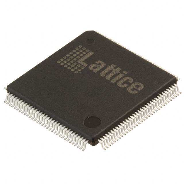
| 产品图片 |
|
| 产品型号 | XC95144XL-7TQG100C |
| rohs | 无铅 / 符合限制有害物质指令(RoHS)规范要求 |
| 产品系列 | XC9500XL |
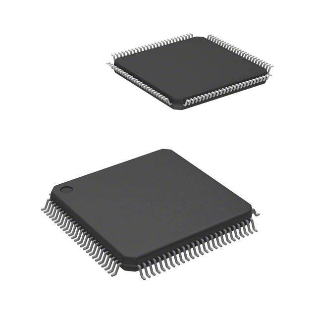
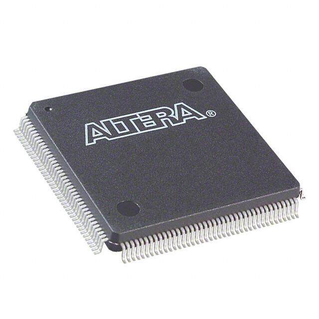
| 供应商器件封装 | 100-TQFP(14x14) |
| 其它名称 | 122-1378 |
| 包装 | 托盘 |
| 可编程类型 | 系统内可编程(最少 10,000 次编程/擦除循环) |
| 安装类型 | 表面贴装 |
| 宏单元数 | 144 |
| 封装/外壳 | 100-LQFP |
| 工作温度 | 0°C ~ 70°C |
| 延迟时间tpd(1)最大值 | 7.5ns |
| 栅极数 | 3200 |
| 标准包装 | 90 |
| 电源电压-内部 | 3 V ~ 3.6 V |
| 逻辑元件/块数 | 8 |


- 商务部:美国ITC正式对集成电路等产品启动337调查
- 曝三星4nm工艺存在良率问题 高通将骁龙8 Gen1或转产台积电
- 太阳诱电将投资9.5亿元在常州建新厂生产MLCC 预计2023年完工
- 英特尔发布欧洲新工厂建设计划 深化IDM 2.0 战略
- 台积电先进制程称霸业界 有大客户加持明年业绩稳了
- 达到5530亿美元!SIA预计今年全球半导体销售额将创下新高
- 英特尔拟将自动驾驶子公司Mobileye上市 估值或超500亿美元
- 三星加码芯片和SET,合并消费电子和移动部门,撤换高东真等 CEO
- 三星电子宣布重大人事变动 还合并消费电子和移动部门
- 海关总署:前11个月进口集成电路产品价值2.52万亿元 增长14.8%


PDF Datasheet 数据手册内容提取
0 XC95144XL High Performance R CPLD DS056 (v2.0) April 3, 2007 Product Specification 0 0 Features 54V18 Function Blocks, providing 3,200 usable gates with propagation delays of 5ns. See Figure2 for overview. • 5 ns pin-to-pin logic delays Power Estimation • System frequency up to 178 MHz • 144 macrocells with 3,200 usable gates Power dissipation in CPLDs can vary substantially depend- • Available in small footprint packages ing on the system frequency, design application and output - 100-pin TQFP (81 user I/O pins) loading. To help reduce power dissipation, each macrocell - 144-pin TQFP (117 user I/O pins) in a XC9500XL device may be configured for low-power - 144-CSP (117 user I/O pins) mode (from the default high-performance mode). In addi- - Pb-free available for all packages tion, unused product-terms and macrocells are automati- cally deactivated by the software to further conserve power. • Optimized for high-performance 3.3V systems - Low power operation For a general estimate of I , the following equation may be CC - 5V tolerant I/O pins accept 5V, 3.3V, and 2.5V used: signals I (mA) = MC (0.175*PT + 0.345) + MC (0.052*PT CC HS HS LP LP - 3.3V or 2.5V output capability + 0.272) + 0.04 * MC (MC +MC )* f TOG HS LP - Advanced 0.35 micron feature size CMOS where: FastFLASH™ technology MC = # macrocells in high-speed configuration HS • Advanced system features PT = average number of high-speed product terms HS - In-system programmable per macrocell - Superior pin-locking and routability with MC = # macrocells in low power configuration LP FastCONNECT™ II switch matrix PT = average number of low power product terms per LP - Extra wide 54-input Function Blocks macrocell - Up to 90 product-terms per macrocell with f = maximum clock frequency individual product-term allocation MCTOG = average % of flip-flops toggling per clock - Local clock inversion with three global and one (~12%) product-term clocks This calculation was derived from laboratory measurements - Individual output enable per output pin with local of an XC9500XL part filled with 16-bit counters and allowing inversion a single output (the LSB) to be enabled. The actual I - Input hysteresis on all user and boundary-scan pin CC value varies with the design application and should be veri- inputs fied during normal system operation. Figure1 shows the - Bus-hold circuitry on all user pin inputs above estimation in a graphical form. For a more detailed - Full IEEE Standard 1149.1 boundary-scan (JTAG) discussion of power consumption in this device, see Xilinx • Fast concurrent programming • Slew rate control on individual outputs • Enhanced data security features • Excellent quality and reliability - Endurance exceeding 10,000 program/erase cycles - 20 year data retention - ESD protection exceeding 2,000V • Pin-compatible with 5V-core XC95144 device in the 100-pin TQFP package WARNING: Programming temperature range of T = 0° C to +70° C A Description The XC95144XL is a 3.3V CPLD targeted for high-perfor- mance, low-voltage applications in leading-edge communi- cations and computing systems. It is comprised of eight © 1998-2007 Xilinx, Inc. All rights reserved. All Xilinx trademarks, registered trademarks, patents, and disclaimers are as listed at http://www.xilinx.com/legal.htm. All other trademarks and registered trademarks are the property of their respective owners. All specifications are subject to change without notice. DS056 (v2.0) April 3, 2007 www.xilinx.com 1 Product Specification
XC95144XL High Performance CPLD R application note XAPP114, “Understanding XC9500XL CPLD Power.” 250 178 MHz 200 High Performance A) 150 m (C 104 MHz C cal I 100 Low Power pi y T 50 0 50 100 150 200 Clock Frequency (MHz) Figure 1: Typical I vs. Frequency for XC95144XL CC 2 www.xilinx.com DS056 (v2.0) April 3, 2007 Product Specification
R XC95144XL High Performance CPLD 3 JTAG JTAG Port 1 In-System Programming Controller Controller 54 Function I/O 18 Block 1 Macrocells I/O 1 to 18 I/O I/O atrix 54 Function M 18 Block 2 h c Macrocells I/O wit 1 to 18 S Blocks T II I/O C E 54 N Function I/O N O 18 Block 3 C I/O st Macrocells a 1 to 18 F I/O 3 I/O/GCK 54 Function 1 I/O/GSR 18 Block 4 4 Macrocells I/O/GTS 1 to 18 54 Function 18 Block 8 Macrocells 1 to 18 DS056_02_101300 Figure 2: XC95144XL Architecture Function Block outputs (indicated by the bold line) drive the I/O Blocks directly. DS056 (v2.0) April 3, 2007 www.xilinx.com 3 Product Specification
XC95144XL High Performance CPLD R Absolute Maximum Ratings(2) Symbol Description Value Units V Supply voltage relative to GND –0.5 to 4.0 V CC V Input voltage relative to GND(1) –0.5 to 5.5 V IN V Voltage applied to 3-state output(1) –0.5 to 5.5 V TS T Storage temperature (ambient)(3) –65 to +150 oC STG T Junction temperature +150 oC J Notes: 1. Maximum DC undershoot below GND must be limited to either 0.5V or 10 mA, whichever is easier to achieve. During transitions, the device pins may undershoot to –2.0 V or overshoot to +7.0V, provided this over- or undershoot lasts less than 10 ns and with the forcing current being limited to 200 mA. External I/O voltage may not exceed V by 4.0V. CCINT 2. Stresses beyond those listed under Absolute Maximum Ratings may cause permanent damage to the device. These are stress ratings only, and functional operation of the device at these or any other conditions beyond those listed under Operating Conditions is not implied. Exposure to Absolute Maximum Ratings conditions for extended periods of time may affect device reliability. 3. For soldering guidelines and thermal considerations, see the Device Packaging information on the Xilinx website. For Pb-free packages, see XAPP427. Recommended Operation Conditions Symbol Parameter Min Max Units V Supply voltage for internal logic Commercial T = 0oC to 70oC 3.0 3.6 V CCINT A and input buffers Industrial T = –40oC to +85oC 3.0 3.6 V A V Supply voltage for output drivers for 3.3V operation 3.0 3.6 V CCIO Supply voltage for output drivers for 2.5V operation 2.3 2.7 V V Low-level input voltage 0 0.80 V IL V High-level input voltage 2.0 5.5 V IH V Output voltage 0 V V O CCIO Quality and Reliability Characteristics Symbol Parameter Min Max Units T Data Retention 20 - Years DR N Program/Erase Cycles (Endurance) 10,000 - Cycles PE V Electrostatic Discharge (ESD) 2,000 - Volts ESD DC Characteristic Over Recommended Operating Conditions Symbol Parameter Test Conditions Min Max Units V Output high voltage for 3.3V outputs I = –4.0 mA 2.4 - V OH OH Output high voltage for 2.5V outputs I = –500 μA 90% V - V OH CCIO V Output low voltage for 3.3V outputs I = 8.0 mA - 0.4 V OL OL Output low voltage for 2.5V outputs I = 500 μA - 0.4 V OL I Input leakage current V = Max; V = GND or V - ±10 μA IL CC IN CC I I/O high-Z leakage current V = Max; V = GND or V - ±10 μA IH CC IN CC 4 www.xilinx.com DS056 (v2.0) April 3, 2007 Product Specification
R XC95144XL High Performance CPLD Symbol Parameter Test Conditions Min Max Units I I/O high-Z leakage current V = Max; V = Max; - ±10 μA IH CC CCIO V = GND or 3.6V IN V Min < V < 5.5V - ±50 μA CC IN C I/O capacitance V = GND; f = 1.0 MHz - 10 pF IN IN I Operating supply current V = GND, No load; f = 1.0 MHz 45 (Typical) mA CC IN (low power mode, active) AC Characteristics XC95144XL-5 XC95144XL-7 XC95144XL-10 Symbol Parameter Min Max Min Max Min Max Units T I/O to output valid - 5.0 - 7.5 - 10.0 ns PD T I/O setup time before GCK 3.7 - 4.8 - 6.5 - ns SU T I/O hold time after GCK 0 - 0 - 0 - ns H T GCK to output valid - 3.5 - 4.5 - 5.8 ns CO f Multiple FB internal operating frequency - 178.6 - 125.0 - 100.0 MHz SYSTEM T I/O setup time before p-term clock input 1.7 - 1.6 - 2.1 - ns PSU T I/O hold time after p-term clock input 2.0 - 3.2 - 4.4 - ns PH T P-term clock output valid - 5.5 - 7.7 - 10.2 ns PCO T GTS to output valid - 4.0 - 5.0 - 7.0 ns OE T GTS to output disable - 4.0 - 5.0 - 7.0 ns OD T Product term OE to output enabled - 7.0 - 9.5 - 11.0 ns POE T Product term OE to output disabled - 7.0 - 9.5 - 11.0 ns POD T GSR to output valid - 10.0 - 12.0 - 14.5 ns AO T P-term S/R to output valid - 10.5 - 12.6 - 15.3 ns PAO T GCK pulse width (High or Low) 2.8 - 4.0 - 4.5 - ns WLH T Asynchronous preset/reset pulse width 5.0 - 6.5 - 7.0 - ns APRPW (High or Low) T P-term clock pulse width (High or Low) 5.0 - 6.5 - 7.0 - ns PLH VTEST R1 Output Type VCCIO VTEST R1 R2 CL Device Output 3.3V 3.3V 320 Ω 360 Ω 35 pF 2.5V 2.5V 250 Ω 660 Ω 35 pF R2 CL DS058_03_081500 Figure 3: AC Load Circuit DS056 (v2.0) April 3, 2007 www.xilinx.com 5 Product Specification
XC95144XL High Performance CPLD R Internal Timing Parameters XC95144XL-5 XC95144XL-7 XC95144XL-10 Symbol Parameter Min Max Min Max Min Max Units Buffer Delays T Input buffer delay - 1.5 - 2.3 - 3.5 ns IN T GCK buffer delay - 1.1 - 1.5 - 1.8 ns GCK T GSR buffer delay - 2.0 - 3.1 - 4.5 ns GSR T GTS buffer delay - 4.0 - 5.0 - 7.0 ns GTS T Output buffer delay - 2.0 - 2.5 - 3.0 ns OUT T Output buffer enable/disable - 0 - 0 - 0 ns EN delay Product Term Control Delays T Product term clock delay - 1.6 - 2.4 - 2.7 ns PTCK T Product term set/reset delay - 1.0 - 1.4 - 1.8 ns PTSR T Product term 3-state delay - 5.5 - 7.2 - 7.5 ns PTTS Internal Register and Combinatorial Delays T Combinatorial logic propagation delay - 0.5 - 1.3 - 1.7 ns PDI T Register setup time 2.3 - 2.6 - 3.0 - ns SUI T Register hold time 1.4 - 2.2 - 3.5 - ns HI T Register clock enable setup time 2.3 - 2.6 - 3.0 - ns ECSU T Register clock enable hold time 1.4 - 2.2 - 3.5 - ns ECHO T Register clock to output valid time - 0.4 - 0.5 - 1.0 ns COI T Register async. S/R to output delay - 6.0 - 6.4 - 7.0 ns AOI T Register async. S/R recover before clock 5.0 7.5 10.0 ns RAI T Internal logic delay - 1.0 - 1.4 - 1.8 ns LOGI T Internal low power logic delay - 5.0 - 6.4 - 7.3 ns LOGILP Feedback Delays T Fast CONNECT II feedback delay - 1.9 - 3.5 - 4.2 ns F Time Adders T Incremental product term allocator delay - 0.7 - 0.8 - 1.0 ns PTA T Slew-rate limited delay - 3.0 - 4.0 - 4.5 ns SLEW 6 www.xilinx.com DS056 (v2.0) April 3, 2007 Product Specification
R XC95144XL High Performance CPLD XC95144XL I/O Pins(2) Function Macro- BScan Function Macro- BScan Block cell TQ100 TQ144 CS144 Order Block cell TQ100 TQ144 CS144 Order 1 1 - 23 H3 429 3 1 - 39 M3 321 1 2 11 16 F1 426 3 2(1) 23(1) 32(1) L1(1) 318 1 3 12 17 G2 423 3 3 - 41 K4 315 1 4 - 25 J1 420 3 4 - 44 N4 312 1 5 13 19 G3 417 3 5 24 33 L2 309 1 6 14 20 G4 414 3 6 25 34 L3 306 1 7 - - - 411 3 7 - 46 L5 303 1 8 15 21 H1 408 3 8(1) 27(1) 38(1) N2(1) 300 1 9 16 22 H2 405 3 9 28 40 N3 297 1 10 - 31 K3 402 3 10 - 48 N5 294 1 11 17 24 H4 399 3 11 29 43 M4 291 1 12 18 26 J2 396 3 12 30 45 K5 288 1 13 - - - 393 3 13 - - - 285 1 14 19 27 J3 390 3 14 32 49 K6 282 1 15 20 28 J4 387 3 15 33 50 L6 279 1 16 - 35 M1 384 3 16 - - - 276 1 17(1) 22(1) 30(1) K2(1) 381 3 17 34 51 M6 273 1 18 - - - 378 3 18 - - - 270 2 1 - 142 C3 375 4 1 - 118 C9 267 2 2(1) 99(1) 143(1) A2(1) 372 4 2 87 126 A7 264 2 3 - - - 369 4 3 - 133 A5 261 2 4 - 4 C1 366 4 4 - - - 258 2 5(1) 1(1) 2(1) B1(1) 363 4 5 89 128 D7 255 2 6(1) 2(1) 3(1) C2(1) 360 4 6 90 129 A6 252 2 7 - - - 357 4 7 - - - 249 2 8(1) 3(1) 5(1) D4(1) 354 4 8 91 130 B6 246 2 9(1) 4(1) 6(1) D3(1) 351 4 9 92 131 C6 243 2 10 - 7 D2 348 4 10 - 135 C5 240 2 11 6 9 E4 345 4 11 93 132 D6 237 2 12 7 10 E3 342 4 12 94 134 B5 234 2 13 - 12 E1 339 4 13 - 137 A4 231 2 14 8 11 E2 336 4 14 95 136 D5 228 2 15 9 13 F4 333 4 15 96 138 B4 225 2 16 - 14 F3 330 4 16 - 139 C4 222 2 17 10 15 F2 327 4 17 97 140 A3 219 2 18 - - - 324 4 18 - - - 216 Notes: 1. Global control pin. 2. The pin-outs are the same for Pb-free versions of packages. DS056 (v2.0) April 3, 2007 www.xilinx.com 7 Product Specification
XC95144XL High Performance CPLD R XC95144XL (Continued) Function Macro- BScan Function Macro- BScan Block cell TQ100 TQ144 CS144 Order Block cell TQ100 TQ144 CS144 Order 5 1 - - - 213 7 1 - - - 105 5 2 35 52 N6 210 7 2 50 71 N12 102 5 3 - 59 L8 207 7 3 - 75 L12 99 5 4 - - - 204 7 4 - - - 96 5 5 36 53 M7 201 7 5 52 74 M13 93 5 6 37 54 N7 198 7 6 53 76 L13 90 5 7 - 66 M10 195 7 7 - 77 K10 87 5 8 39 56 K7 192 7 8 54 78 K11 84 5 9 40 57 N8 189 7 9 55 80 K13 81 5 10 –- 68 N11 186 7 10 - 79 K12 78 5 11 41 58 M8 183 7 11 56 82 J11 75 5 12 42 60 K8 180 7 12 58 85 H10 72 5 13 - 70 L11 177 7 13 - 81 J10 69 5 14 43 61 N9 174 7 14 59 86 H11 66 5 15 46 64 K9 171 7 15 60 87 H12 63 5 16 - - - 168 7 16 - 83 J12 60 5 17 49 69 M11 165 7 17 61 88 H13 57 5 18 - - - 162 7 18 - - - 54 6 1 - - - 159 8 1 - - - 51 6 2 74 106 C11 156 8 2 63 91 G11 48 6 3 - - - 153 8 3 - 95 F11 45 6 4 - 111 B11 150 8 4 - 97 E13 42 6 5 76 110 A12 147 8 5 64 92 G10 39 6 6 77 112 A11 144 8 6 65 93 F13 36 6 7 - - - 141 8 7 - - - 33 6 8 78 113 D10 138 8 8 66 94 F12 30 6 9 79 116 A10 135 8 9 67 96 F10 27 6 10 - 115 B10 132 8 10 - 101 D13 24 6 11 80 119 B9 129 8 11 68 98 E12 21 6 12 81 120 A9 126 8 12 70 100 E10 18 6 13 - - - 123 8 13 - 103 D11 15 6 14 82 121 D8 120 8 14 71 102 D12 12 6 15 85 124 A8 117 8 15 72 104 C13 9 6 16 - 117 D9 114 8 16 - 107 B13 6 6 17 86 125 B7 111 8 17 73 105 C12 3 6 18 - - - 108 8 18 - - - 0 Notes: 1. The pin-outs are the same for Pb-free versions of packages. 8 www.xilinx.com DS056 (v2.0) April 3, 2007 Product Specification
R XC95144XL High Performance CPLD XC95144XL Global, JTAG and Power Pins(1) Pin Type TQ100 TQ144 CS144 I/O/GCK1 22 30 K2 I/O/GCK2 23 32 L1 I/O/GCK3 27 38 N2 I/O/GTS1 3 5 D4 I/O/GTS2 4 6 D3 I/O/GTS3 1 2 B1 I/O/GTS4 2 3 C2 I/O/GSR 99 143 A2 TCK 48 67 L10 TDI 45 63 L9 TDO 83 122 C8 TMS 47 65 N10 V 3.3V 5, 57, 98 8, 42, 84, 141 B3, D1, J13, L4 CCINT V 2.5V/3.3V 26, 38, 51, 88 1, 37, 55, 73, 109, 127 A1, A13, C7, L7, N1, N13 CCIO GND 21, 31, 44, 62, 69, 75, 84, 100 18, 29, 36, 47, 62, 72, 89, 90, 99, B2, B8, B12, C10, E11, G1, G12, 108, 114, 123, 144 G13, K1, M2, M5, M9, M12 No Connects - – – Notes: 1. The pin-outs are the same for Pb-free versions of packages. DS056 (v2.0) April 3, 2007 www.xilinx.com 9 Product Specification
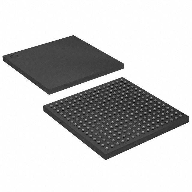
XC95144XL High Performance CPLD R Device Part Marking and Ordering Combination Information. R Device Type XC95xxxXL Package TQ144 This line not Speed 7C related to device part number Operating Range 1 Sample package with part marking. Speed Device Ordering and (pin-to-pin Pkg. No. of Operating Part Marking Number delay) Symbol Pins Package Type Range(1) XC95144XL-5TQ100C 5 ns TQ100 100-pin Thin Quad Flat Pack (TQFP) C XC95144XL-5TQ144C 5 ns TQ144 144-pin Thin Quad Flat Pack (TQFP) C XC95144XL-5CS144C 5 ns CS144 144-ball Chip Scale Package (CSP) C XC95144XL-7TQ100C 7.5 ns TQ100 100-pin Thin Quad Flat Pack (TQFP) C XC95144XL-7TQ144C 7.5 ns TQ144 144-pin Thin Quad Flat Pack (TQFP) C XC95144XL-7CS144C 7.5 ns CS144 144-ball Chip Scale Package (CSP) C XC95144XL-7TQ100I 7.5 ns TQ100 100-pin Thin Quad Flat Pack (TQFP) I XC95144XL-7TQ144I 7.5 ns TQ144 144-pin Thin Quad Flat Pack (TQFP) I XC95144XL-7CS144I 7.5 ns CS144 144-ball Chip Scale Package (CSP) I XC95144XL-10TQ100C 10 ns TQ100 100-pin Thin Quad Flat Pack (TQFP) C XC95144XL-10TQ144C 10 ns TQ144 144-pin Thin Quad Flat Pack (TQFP) C XC95144XL-10CS144C 10 ns CS144 144-ball Chip Scale Package (CSP) C XC95144XL-10TQ100I 10 ns TQ100 100-pin Thin Quad Flat Pack (TQFP) I XC95144XL-10TQ144I 10 ns TQ144 144-pin Thin Quad Flat Pack (TQFP) I XC95144XL-10CS144I 10 ns CS144 144-ball Chip Scale Package (CSP) I XC95144XL-5TQG100C 5 ns TQG100 100-pin Thin Quad Flat Pack (TQFP); Pb-free C XC95144XL-5TQG144C 5 ns TQG144 144-pin Thin Quad Flat Pack (TQFP); Pb-free C XC95144XL-5CSG144C 5 ns CSG144 144-ball Chip Scale Package (CSP); Pb-free C XC95144XL-7TQG100C 7.5 ns TQG100 100-pin Thin Quad Flat Pack (TQFP); Pb-free C XC95144XL-7TQG144C 7.5 ns TQG144 144-pin Thin Quad Flat Pack (TQFP); Pb-free C XC95144XL-7CSG144C 7.5 ns CSG144 144-ball Chip Scale Package (CSP); Pb-free C XC95144XL-7TQG100I 7.5 ns TQG100 100-pin Thin Quad Flat Pack (TQFP); Pb-free I XC95144XL-7TQG144I 7.5 ns TQG144 144-pin Thin Quad Flat Pack (TQFP); Pb-free I XC95144XL-7CSG144I 7.5 ns CSG144 144-ball Chip Scale Package (CSP); Pb-free I 10 www.xilinx.com DS056 (v2.0) April 3, 2007 Product Specification
R XC95144XL High Performance CPLD Speed Device Ordering and (pin-to-pin Pkg. No. of Operating Part Marking Number delay) Symbol Pins Package Type Range(1) XC95144XL-10TQG100C 10 ns TQG100 100-pin Thin Quad Flat Pack (TQFP); Pb-free C XC95144XL-10TQG144C 10 ns TQG144 144-pin Thin Quad Flat Pack (TQFP); Pb-free C XC95144XL-10CSG144C 10 ns CSG144 144-ball Chip Scale Package (CSP); Pb-free C XC95144XL-10TQG100I 10 ns TQG100 100-pin Thin Quad Flat Pack (TQFP); Pb-free I XC95144XL-10TQG144I 10 ns TQG144 144-pin Thin Quad Flat Pack (TQFP); Pb-free I XC95144XL-10CSG144I 10 ns CSG144 144-ball Chip Scale Package (CSP); Pb-free I Notes: 1. C = Commercial: T = 0° to +70°C; I = Industrial: T = –40° to +85°C A A Standard Example: X C 9 5 1 4 4XL - 4 TQ 144 C Pb-Free Example: X C 9 5 1 4 4XL -4 TQ G 144 C Device Device Speed Grade Speed Grade Package Type Package Type Number of Pins Pb-Free Temperature Range Number of Pins Temperature Range Warranty Disclaimer THESE PRODUCTS ARE SUBJECT TO THE TERMS OF THE XILINX LIMITED WARRANTY WHICH CAN BE VIEWED AT http://www.xilinx.com/warranty.htm. THIS LIMITED WARRANTY DOES NOT EXTEND TO ANY USE OF THE PRODUCTS IN AN APPLICATION OR ENVIRONMENT THAT IS NOT WITHIN THE SPECIFICATIONS STATED ON THE THEN-CURRENT XILINX DATA SHEET FOR THE PRODUCTS. PRODUCTS ARE NOT DESIGNED TO BE FAIL-SAFE AND ARE NOT WARRANTED FOR USE IN APPLICATIONS THAT POSE A RISK OF PHYSICAL HARM OR LOSS OF LIFE. USE OF PRODUCTS IN SUCH APPLICATIONS IS FULLY AT THE RISK OF CUSTOMER SUBJECT TO APPLICABLE LAWS AND REGULATIONS. Further Reading The following Xilinx links go to relevant XC9500XL CPLD documentation, including XAPP111, Using the XC9500XL Timing Model, and XAPP784, Bulletproof CPLD Design Practices. Simply click on the link and scroll down. Data Sheets, Application Notes, and White Papers. Packaging DS056 (v2.0) April 3, 2007 www.xilinx.com 11 Product Specification
XC95144XL High Performance CPLD R Revision History The following table shows the revision history for this document. Date Version Revision 10/30/98 1.1 Minor corrections to CS144 pinout table. 11/13/98 1.2 V1.2 minor correction in CS144 pinout table. 06/20/02 1.3 Updated I equation, page 1. Updated DC Characteristics: I to 45 (typical). Updated CC CC Component Availability chart.Added additional I test conditions and measurements to DC IH Characteristics table. 06/20/03 1.4 Updated T from 260 to 220oC. Added Part Marking and updated Ordering Information. SOL 08/21/03 1.5 Updated Package Device Marking Pin 1 orientation. 07/15/04 1.6 Added Pb-free documentation 09/15/04 1.7 Added T specification to AC Characteristics. APRPW 07/15/05 1.8 Move to Product Specification 03/22/06 1.9 Add Warranty Disclaimer. 04/03/07 2.0 Add programming temperature range warning on page 1. 12 www.xilinx.com DS056 (v2.0) April 3, 2007 Product Specification