ICGOO在线商城 > 集成电路(IC) > 嵌入式 - FPGA(现场可编程门阵列) > XC5VLX30-1FFG324C
 Datasheet下载
- 型号: XC5VLX30-1FFG324C
- 制造商: Xilinx
- 库位|库存: xxxx|xxxx
- 要求:
| 数量阶梯 | 香港交货 | 国内含税 |
| +xxxx | $xxxx | ¥xxxx |
查看当月历史价格
查看今年历史价格
XC5VLX30-1FFG324C产品简介:
ICGOO电子元器件商城为您提供XC5VLX30-1FFG324C由Xilinx设计生产,在icgoo商城现货销售,并且可以通过原厂、代理商等渠道进行代购。 XC5VLX30-1FFG324C价格参考。XilinxXC5VLX30-1FFG324C封装/规格:嵌入式 - FPGA(现场可编程门阵列), 。您可以下载XC5VLX30-1FFG324C参考资料、Datasheet数据手册功能说明书,资料中有XC5VLX30-1FFG324C 详细功能的应用电路图电压和使用方法及教程。
Xilinx Inc.的XC5VLX30-1FFG324C属于Virtex-5系列FPGA,是一款高性能、高密度的现场可编程门阵列。其应用场景主要包括以下几个方面:

 1. 通信领域
   - 无线通信:用于基带处理、信号调制解调、协议加速等任务,支持复杂的通信算法。
   - 光通信:实现高速数据传输中的帧处理、前向纠错(FEC)、时钟数据恢复等功能。
   - 网络设备:应用于路由器、交换机和防火墙中,提供灵活的数据包处理和流量管理能力。

 2. 图像与视频处理
   - 实时图像处理:支持高清视频流的编码、解码、图像增强和格式转换。
   - 嵌入式视觉系统:用于工业相机、无人机和医疗成像设备中的图像分析和目标检测。

 3. 工业自动化
   - 运动控制:通过精确的时序控制和并行处理能力,实现多轴运动协调。
   - 实时数据采集:用于传感器数据的高速采集、滤波和预处理。
   - 工业通信协议:支持以太网/IP、Profinet等工业标准协议的硬件实现。

 4. 航空航天与国防
   - 雷达信号处理:实现快速傅里叶变换(FFT)、脉冲压缩和其他复杂算法。
   - 导航与制导:用于惯性导航系统中的数据融合和轨迹计算。
   - 加密与安全:提供硬件级别的数据加密和解密功能,保障通信安全。

 5. 医疗设备
   - 医学成像:用于超声、CT和MRI设备中的信号处理和图像重建。
   - 生命体征监测:实现多通道数据采集和实时分析。

 6. 科学计算与研究
   - 高性能计算(HPC):通过并行计算加速复杂数学模型的求解。
   - 基因测序:支持大规模数据的快速比对和分析。

 7. 消费电子
   - 音频/视频编解码:用于家庭娱乐设备中的多媒体处理。
   - 游戏开发:为图形渲染和物理引擎提供硬件加速。

XC5VLX30-1FFG324C凭借其强大的逻辑资源、丰富的I/O接口以及嵌入式处理器支持,能够满足多种复杂应用场景的需求,同时具备高度灵活性和可重构性,适用于需要高性能和定制化解决方案的领域。
| 参数 | 数值 |
| 产品目录 | 集成电路 (IC) |
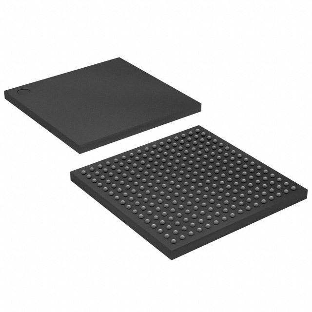
| 描述 | IC FPGA 220 I/O 324FBGA |
| 产品分类 | |
| I/O数 | 220 |
| LAB/CLB数 | 2400 |
| 品牌 | Xilinx Inc |
| 数据手册 | |
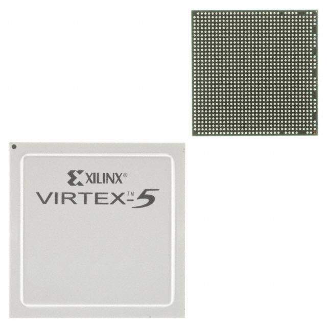
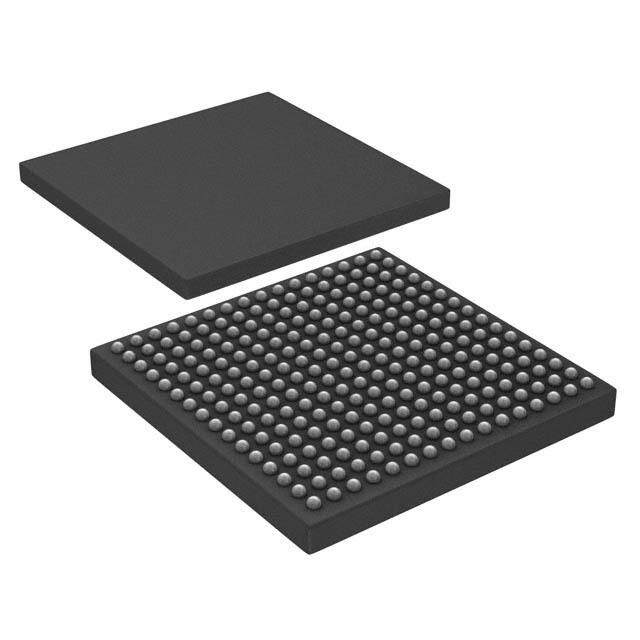
| 产品图片 |
|
| 产品型号 | XC5VLX30-1FFG324C |
| rohs | 无铅 / 符合限制有害物质指令(RoHS)规范要求 |
| 产品系列 | Virtex®-5 LX |
| 供应商器件封装 | 324-FCBGA(19x19) |
| 其它名称 | 122-1558 |
| 安装类型 | 表面贴装 |
| 封装/外壳 | 324-BBGA,FCBGA |
| 工作温度 | 0°C ~ 85°C |
| 总RAM位数 | 1179648 |
| 栅极数 | - |
| 标准包装 | 84 |
| 电压-电源 | 0.95 V ~ 1.05 V |
| 逻辑元件/单元数 | 30720 |
| 配用 | /product-detail/zh/HW-AFX-FF324-500-G/HW-AFX-FF324-500-G-ND/1769268/product-detail/zh/DAC1408D750W1%2FDB,598/568-5088-ND/2295306 |


- 商务部:美国ITC正式对集成电路等产品启动337调查
- 曝三星4nm工艺存在良率问题 高通将骁龙8 Gen1或转产台积电
- 太阳诱电将投资9.5亿元在常州建新厂生产MLCC 预计2023年完工
- 英特尔发布欧洲新工厂建设计划 深化IDM 2.0 战略
- 台积电先进制程称霸业界 有大客户加持明年业绩稳了
- 达到5530亿美元!SIA预计今年全球半导体销售额将创下新高
- 英特尔拟将自动驾驶子公司Mobileye上市 估值或超500亿美元
- 三星加码芯片和SET,合并消费电子和移动部门,撤换高东真等 CEO
- 三星电子宣布重大人事变动 还合并消费电子和移动部门
- 海关总署:前11个月进口集成电路产品价值2.52万亿元 增长14.8%

PDF Datasheet 数据手册内容提取
0 R Virtex-5 Family Overview DS100 (v5.1) August 21, 2015 Product Specification 0 0 General Description Using the second generation ASMBL™ (Advanced Silicon Modular Block) column-based architecture, the Virtex-5 family contains five distinct platforms (sub-families), the most choice offered by any FPGA family. Each platform contains a different ratio of features to address the needs of a wide variety of advanced logic designs. In addition to the most advanced, high-performance logic fabric, Virtex-5FPGAs contain many hard-IP system level blocks, including powerful 36-Kbit block RAM/FIFOs, second generation 25x18 DSP slices, SelectIO™ technology with built-in digitally-controlled impedance, ChipSync™ source-synchronous interface blocks, system monitor functionality, enhanced clock management tiles with integrated DCM (Digital Clock Managers) and phase-locked-loop (PLL) clock generators, and advanced configuration options. Additional platform dependant features include power-optimized high-speed serial transceiver blocks for enhanced serial connectivity, PCIExpress® compliant integrated Endpoint blocks, tri-mode Ethernet MACs (Media Access Controllers), and high-performance PowerPC®440 microprocessor embedded blocks. These features allow advanced logic designers to build the highest levels of performance and functionality into their FPGA-based systems. Built on a 65-nm state-of-the-art copper process technology, Virtex-5 FPGAs are a programmable alternative to custom ASIC technology. Most advanced system designs require the programmable strength of FPGAs. Virtex-5 FPGAs offer the best solution for addressing the needs of high-performance logic designers, high-performance DSP designers, and high-performance embedded systems designers with unprecedented logic, DSP, hard/soft microprocessor, and connectivity capabilities. The Virtex-5 LXT, SXT, TXT, and FXT platforms include advanced high-speed serial connectivity and link/transaction layer capability. Summary of Virtex-5 FPGA Features • Five platforms LX, LXT, SXT, TXT, and FXT • Advanced DSP48E slices − Virtex-5 LX: High-performance general logic applications − 25x18, two’s complement, multiplication − Virtex-5 LXT: High-performance logic with advanced serial − Optional adder, subtracter, and accumulator connectivity − Optional pipelining − Virtex-5 SXT: High-performance signal processing − Optional bitwise logical functionality applications with advanced serial connectivity − Dedicated cascade connections − Virtex-5 TXT: High-performance systems with double • Flexible configuration options density advanced serial connectivity − SPI and Parallel FLASH interface − Virtex-5 FXT: High-performance embedded systems with − Multi-bitstream support with dedicated fallback advanced serial connectivity reconfiguration logic • Cross-platform compatibility − Auto bus width detection capability − LXT, SXT, and FXT devices are footprint compatible in the • System Monitoring capability on all devices same package using adjustable voltage regulators • Most advanced, high-performance, optimal-utilization, − On-chip/Off-chip thermal monitoring FPGA fabric − On-chip/Off-chip power supply monitoring − Real 6-input look-up table (LUT) technology − JTAG access to all monitored quantities − Dual 5-LUT option • Integrated Endpoint blocks for PCI Express Designs − Improved reduced-hop routing − LXT, SXT, TXT, and FXT Platforms − 64-bit distributed RAM option − Compliant with the PCI Express Base Specification 1.1 − SRL32/Dual SRL16 option −− xW1o, rxk4s, ionr cxo8n ljaunnect isounp wpoitrht pReorc bkelotcIOk™ transceivers • Powerful clock management tile (CMT) clocking • Tri-mode 10/100/1000 Mb/s Ethernet MACs − Digital Clock Manager (DCM) blocks for zero delay − LXT, SXT, TXT, and FXT Platforms buffering, frequency synthesis, and clock phase shifting − RocketIO transceivers can be used as PHY or connect to − PLL blocks for input jitter filtering, zero delay buffering, external PHY using many soft MII (Media Independent frequency synthesis, and phase-matched clock division Interface) options • 36-Kbit block RAM/FIFOs • RocketIO GTP transceivers 100Mb/s to 3.75Gb/s − True dual-port RAM blocks − LXT and SXT Platforms − Enhanced optional programmable FIFO logic • RocketIO GTX transceivers 150Mb/s to 6.5Gb/s − Programmable − TXT and FXT Platforms - True dual-port widths up to x36 • PowerPC 440 Microprocessors - Simple dual-port widths up to x72 − FXT Platform only − Built-in optional error-correction circuitry − RISC architecture − Optionally program each block as two independent 18-Kbit − 7-stage pipeline blocks − 32-Kbyte instruction and data caches included • High-performance parallel SelectIO technology − Optimized processor interface structure (crossbar) − 1.2 to 3.3V I/O Operation • 65-nm copper CMOS process technology − Source-synchronous interfacing using ChipSync™ • 1.0V core voltage • High signal-integrity flip-chip packaging available in standard technology − Digitally-controlled impedance (DCI) active termination or Pb-free package options − Flexible fine-grained I/O banking − High-speed memory interface support © 2006–2015 Xilinx, Inc., Xilinx, the Xilinx logo, Artix, ISE, Kintex, Spartan, UltraScale, Virtex, Vivado, Zynq, and other designated brands included herein are trademarks of Xilinx in the United States and other countries. PCI, PCIe, and PCI Express are trademarks of PCI-SIG and used under license. PowerPC is a trademark of IBM Corp. and is used under license. All other trademarks are the property of their respective owners. DS100 (v5.1) August 21, 2015 www.xilinx.com Product Specification 1
Virtex-5 Family Overview R Table 1: Virtex-5 FPGA Family Members Configurable Logic Blocks (CLBs) Block RAM Blocks Max RocketIO PowerPC Endpoint Transceivers(6) Total Max Device (RoAwr rxa yCol) SVliircteexs-(15) DistMriabxuted SDlSicPe4s8(2E) 18Kb(3) 36Kb (MKabx) CMTs(4) PrBolcoecskssor BEloxPcpkCrseI sfsor EMtAheCrsn(e5)t GTP GTX BanI/Oks(8) IU/Ose(7r) RAM(Kb) XC5VLX30 80x30 4,800 320 32 64 32 1,152 2 N/A N/A N/A N/A N/A 13 400 XC5VLX50 120x30 7,200 480 48 96 48 1,728 6 N/A N/A N/A N/A N/A 17 560 XC5VLX85 120x54 12,960 840 48 192 96 3,456 6 N/A N/A N/A N/A N/A 17 560 XC5VLX110 160x54 17,280 1,120 64 256 128 4,608 6 N/A N/A N/A N/A N/A 23 800 XC5VLX155 160x76 24,320 1,640 128 384 192 6,912 6 N/A N/A N/A N/A N/A 23 800 XC5VLX220 160x108 34,560 2,280 128 384 192 6,912 6 N/A N/A N/A N/A N/A 23 800 XC5VLX330 240x108 51,840 3,420 192 576 288 10,368 6 N/A N/A N/A N/A N/A 33 1,200 XC5VLX20T 60x26 3,120 210 24 52 26 936 1 N/A 1 2 4 N/A 7 172 XC5VLX30T 80x30 4,800 320 32 72 36 1,296 2 N/A 1 4 8 N/A 12 360 XC5VLX50T 120x30 7,200 480 48 120 60 2,160 6 N/A 1 4 12 N/A 15 480 XC5VLX85T 120x54 12,960 840 48 216 108 3,888 6 N/A 1 4 12 N/A 15 480 XC5VLX110T 160x54 17,280 1,120 64 296 148 5,328 6 N/A 1 4 16 N/A 20 680 XC5VLX155T 160x76 24,320 1,640 128 424 212 7,632 6 N/A 1 4 16 N/A 20 680 XC5VLX220T 160x108 34,560 2,280 128 424 212 7,632 6 N/A 1 4 16 N/A 20 680 XC5VLX330T 240x108 51,840 3,420 192 648 324 11,664 6 N/A 1 4 24 N/A 27 960 XC5VSX35T 80x34 5,440 520 192 168 84 3,024 2 N/A 1 4 8 N/A 12 360 XC5VSX50T 120x34 8,160 780 288 264 132 4,752 6 N/A 1 4 12 N/A 15 480 XC5VSX95T 160x46 14,720 1,520 640 488 244 8,784 6 N/A 1 4 16 N/A 19 640 XC5VSX240T 240x78 37,440 4,200 1,056 1,032 516 18,576 6 N/A 1 4 24 N/A 27 960 XC5VTX150T 200x58 23,200 1,500 80 456 228 8,208 6 N/A 1 4 N/A 40 20 680 XC5VTX240T 240x78 37,440 2,400 96 648 324 11,664 6 N/A 1 4 N/A 48 20 680 XC5VFX30T 80x38 5,120 380 64 136 68 2,448 2 1 1 4 N/A 8 12 360 XC5VFX70T 160x38 11,200 820 128 296 148 5,328 6 1 3 4 N/A 16 19 640 XC5VFX100T 160x56 16,000 1,240 256 456 228 8,208 6 2 3 4 N/A 16 20 680 XC5VFX130T 200x56 20,480 1,580 320 596 298 10,728 6 2 3 6 N/A 20 24 840 XC5VFX200T 240x68 30,720 2,280 384 912 456 16,416 6 2 4 8 N/A 24 27 960 Notes: 1. Virtex-5 FPGA slices are organized differently from previous generations. Each Virtex-5 FPGA slice contains four LUTs and four flip-flops (previously it was two LUTs and two flip-flops.) 2. Each DSP48E slice contains a 25x18 multiplier, an adder, and an accumulator. 3. Block RAMs are fundamentally 36Kbits in size. Each block can also be used as two independent 18-Kbit blocks. 4. Each Clock Management Tile (CMT) contains two DCMs and one PLL. 5. This table lists separate Ethernet MACs per device. 6. RocketIO GTP transceivers are designed to run from 100Mb/s to 3.75Gb/s. RocketIO GTX transceivers are designed to run from 150Mb/s to 6.5Gb/s. 7. This number does not include RocketIO transceivers. 8. Includes configuration Bank 0. 2 www.xilinx.com DS100 (v5.1) August 21, 2015 Product Specification
R Virtex-5 Family Overview Virtex-5 FPGA Logic 550 MHz Integrated Block Memory • On average, one to two speed grade improvement over • Up to 16.4Mbits of integrated block memory Virtex-4 devices • 36-Kbit blocks with optional dual 18-Kbit mode • Cascadable 32-bit variable shift registers or 64-bit • True dual-port RAM cells distributed memory capability • Independent port width selection (x1 to x72) • Superior routing architecture with enhanced diagonal − Up to x36 total per port for true dual port operation routing supports block-to-block connectivity with − Up to x72 total per port for simple dual port operation minimal hops (one Read port and one Write port) • Up to 330,000 logic cells including: − Memory bits plus parity/sideband memory support for − Up to 207,360 internal fabric flip-flops with clock enable x9, x18, x36, and x72 widths − Configurations from 32Kx1 to 512x72 (XC5VLX330) − Up to 207,360 real 6-input look-up tables (LUTs) with (8Kx4 to 512x72 for FIFO operation) greater than 13 million total LUT bits • Multirate FIFO support logic − Two outputs for dual 5-LUT mode gives enhanced − Full and Empty flag with fully programmable Almost Full utilization and Almost Empty flags − Logic expanding multiplexers and I/O registers • Synchronous FIFO support without Flag uncertainty • Optional pipeline stages for higher performance 550 MHz Clock Technology • Byte-write capability • Up to six Clock Management Tiles (CMTs) • Dedicated cascade routing to form 64Kx1 memory − Each CMT contains two DCMs and one PLL—up to without using FPGA routing eighteen total clock generators − Flexible DCM-to-PLL or PLL-to-DCM cascade • Integrated optional ECC for high-reliability memory − Precision clock deskew and phase shift requirements − Flexible frequency synthesis • Special reduced-power design for 18Kbit (and below) − Multiple operating modes to ease performance trade-off operation decisions − Improved maximum input/output frequency 550 MHz DSP48E Slices − Fine-grained phase shifting resolution − Input jitter filtering • 25x18 two’s complement multiplication − Low-power operation • Optional pipeline stages for enhanced performance − Wide phase shift range • Optional 48-bit accumulator for multiply accumulate • Differential clock tree structure for optimized low-jitter (MACC) operation with optional accumulator cascade clocking and precise duty cycle to 96-bits • 32 global clock networks • Integrated adder for complex-multiply or multiply-add • Regional, I/O, and local clocks in addition to global operation clocks • Optional bitwise logical operation modes SelectIO Technology • Independent C registers per slice • Up to 1,200 user I/Os • Fully cascadable in a DSP column without external • Wide selection of I/O standards from 1.2V to 3.3V routing resources • Extremely high-performance ChipSync Source-Synchronous − Up to 800Mb/s HSTL and SSTL (on all single-ended I/Os) Interfacing Logic − Up to 1.25Gb/s LVDS (on all differential I/O pairs) • Works in conjunction with SelectIO technology to • True differential termination on-chip simplify source-synchronous interfaces • Same edge capture at input and output I/Os • Per-bit deskew capability built into all I/O blocks • Extensive memory interface support (variable delay line on all inputs and outputs) • Dedicated I/O and regional clocking resources (pins and trees) • Built-in data serializer/deserializer logic with corresponding clock divider support in all I/O • Networking/telecommunication interfaces up to 1.25Gb/s per I/O DS100 (v5.1) August 21, 2015 www.xilinx.com Product Specification 3
Virtex-5 Family Overview R Digitally Controlled Impedance (DCI) System Monitor Active I/O Termination • On-Chip temperature measurement (±4°C) • Optional series or parallel termination • On-Chip power supply measurement (±1%) • Temperature and voltage compensation • Easy to use, self-contained • Makes board layout much easier − No design required for basic operation − Autonomous monitoring of all on-chip sensors − Reduces resistors − User programmable alarm thresholds for on-chip − Places termination in the ideal location, at the signal sensors source or destination • User accessible 10-bit 200kSPS ADC Configuration − Automatic calibration of offset and gain error • Support for platform Flash, standard SPI Flash, or − DNL = ±0.9 LSBs maximum standard parallel NOR Flash configuration • Up to 17 external analog input channels supported • Bitstream support with dedicated fallback − 0V to 1V input range reconfiguration logic − Monitor external sensors e.g., voltage, temperature • 256-bit AES bitstream decryption provides intellectual − General purpose analog inputs property security and prevents design copying • Full access from fabric or JTAG TAP to System Monitor • Improved bitstream error detection/correction capability • Fully operational prior to FPGA configuration and • Auto bus width detection capability during device power down (access via JTAG TAP only) • Partial Reconfiguration via ICAP port 65-nm Copper CMOS Process Advanced Flip-Chip Packaging • 1.0V Core Voltage • Pre-engineered packaging technology for proven • 12-layer metal provides maximum routing capability superior signal integrity and accommodates hard-IP immersion − Minimized inductive loops from signal to return • Triple-oxide technology for proven reduced static power − Optimal signal-to-PWR/GND ratios consumption • Reduces SSO induced noise by up to 7x • Pb-Free and standard packages System Blocks Specific to the LXT, SXT, TXT, and FXT Devices Integrated Endpoint Block for PCI Express Tri-Mode Ethernet Media Access Controller Compliance • Designed to the IEEE 802.3-2002 specification • Works in conjunction with RocketIO GTP transceivers • Operates at 10, 100, and 1,000 Mb/s (LXT and SXT) and GTX transceivers (TXT and FXT) • Supports tri-mode auto-negotiation to deliver full PCI Express Endpoint functionality with • Receive address filter (5 address entries) minimal FPGA logic utilization. • Fully monolithic 1000Base-X solution with RocketIO • Compliant with the PCI Express Base Specification 1.1 GTP transceivers • PCI Express Endpoint block or Legacy PCI Express • Supports multiple external PHY connections (RGMII, Endpoint block GMII, etc.) interfaces through soft logic and SelectIO • x8, x4, or x1 lane width resources • Power management support • Supports connection to external PHY device through • Block RAMs used for buffering SGMII using soft logic and RocketIO GTP transceivers • Fully buffered transmit and receive • Receive and transmit statistics available through • Management interface to access PCI Express separate interface configuration space and internal configuration • Separate host and client interfaces • Supports the full range of maximum payload sizes • Support for jumbo frames • Up to 6x32 bit or 3x64 bit BARs (or a combination of • Support for VLAN 32 bit and 64 bit) • Flexible, user-configurable host interface • Supports IEEE 802.3ah-2004 unidirectional mode 4 www.xilinx.com DS100 (v5.1) August 21, 2015 Product Specification
R Virtex-5 Family Overview RocketIO GTP Transceivers (LXT/SXT only) PowerPC 440 RISC Cores (FXT only) • Full-duplex serial transceiver capable of 100Mb/s to • Embedded PowerPC 440 (PPC440) cores 3.75Gb/s baud rates − Up to 550MHz operation • 8B/10B, user-defined FPGA logic, or no encoding − Greater than 1000 DMIPS per core options − Seven-stage pipeline • Channel bonding support − Multiple instructions per cycle − Out-of-order execution • CRC generation and checking − 32Kbyte, 64-way set associative level 1 instruction • Programmable pre-emphasis or pre-equalization for cache the transmitter − 32Kbyte, 64-way set associative level 1 data cache • Programmable termination and voltage swing − Book E compliant • Programmable equalization for the receiver • Integrated crossbar for enhanced system performance • Receiver signal detect and loss of signal indicator − 128-bit Processor Local Buses (PLBs) − Integrated scatter/gather DMA controllers • User dynamic reconfiguration using secondary − Dedicated interface for connection to DDR2 memory configuration bus controller • Out of Band (OOB) support for Serial ATA (SATA) − Auto-synchronization for non-integer PLB-to-CPU clock • Electrical idle, beaconing, receiver detection, and PCI ratios Express and SATA spread-spectrum clocking support • Auxiliary Processor Unit (APU) Interface and Controller • Less than 100mW typical power consumption − Direct connection from PPC440 embedded block to FPGA fabric-based coprocessors • Built-in PRBS Generators and Checkers − 128-bit wide pipelined APU Load/Store RocketIO GTX Transceivers (TXT/FXT only) − Support of autonomous instructions: no pipeline stalls − Programmable decode for custom instructions • Full-duplex serial transceiver capable of 150Mb/s to 6.5Gb/s baud rates • 8B/10B encoding and programmable gearbox to support 64B/66B and 64B/67B encoding, user-defined FPGA logic, or no encoding options • Channel bonding support • CRC generation and checking • Programmable pre-emphasis or pre-equalization for the transmitter • Programmable termination and voltage swing • Programmable continuous time equalization for the receiver • Programmable decision feedback equalization for the receiver • Receiver signal detect and loss of signal indicator • User dynamic reconfiguration using secondary configuration bus • OOB support (SATA) • Electrical idle, beaconing, receiver detection, and PCI Express spread-spectrum clocking support • Low-power operation at all line rates DS100 (v5.1) August 21, 2015 www.xilinx.com Product Specification 5
Virtex-5 Family Overview R Architectural Description Virtex-5 FPGA Array Overview Virtex-5 devices are user-programmable gate arrays with various configurable elements and embedded cores optimized for high-density and high-performance system designs. Virtex-5 devices implement the following functionality: • I/O blocks provide the interface between package pins Additionally, LXT, SXT, TXT, and FXT devices also contain: and the internal configurable logic. Most popular and • Integrated Endpoint blocks for PCI Express designs leading-edge I/O standards are supported by providing x1, x4, or x8 PCI Express Endpoint programmable I/O blocks (IOBs). The IOBs can be functionality. When used in conjunction with RocketIO connected to very flexible ChipSync logic for enhanced transceivers, a complete PCI Express Endpoint can be source-synchronous interfacing. Source-synchronous implemented with minimal FPGA logic utilization. optimizations include per-bit deskew (on both input and output signals), data serializers/deserializers, clock • 10/100/1000 Mb/s Ethernet media-access control dividers, and dedicated I/O and local clocking blocks offer Ethernet capability. resources. LXT and SXT devices contain: • Configurable Logic Blocks (CLBs), the basic logic • RocketIO GTP transceivers capable of running up to elements for Xilinx® FPGAs, provide combinatorial and 3.75Gb/s. Each GTP transceiver supports full-duplex, synchronous logic as well as distributed memory and clock-and-data recovery. SRL32 shift register capability. Virtex-5 FPGA CLBs are based on real 6-input look-up table technology and TXT and FXT devices contain: provide superior capabilities and performance • GTX transceivers capable of running up to 6.5Gb/s. compared to previous generations of programmable Each GTX transceiver supports full-duplex, clock-and- logic. data recovery. • Block RAM modules provide flexible 36Kbit true dual- FXT devices contain: port RAM that are cascadable to form larger memory blocks. In addition, Virtex-5 FPGA block RAMs contain • Embedded IBM PowerPC 440 RISC CPUs. Each optional programmable FIFO logic for increased device PowerPC 440 CPU is capable of running up to utilization. Each block RAM can also be configured as 550MHz. Each PowerPC 440 CPU also has an APU two independent 18Kbit true dual-port RAM blocks, (Auxiliary Processor Unit) interface that supports providing memory granularity for designs needing hardware acceleration, and an integrated cross-bar for smaller RAM blocks. high data throughput. • Cascadable embedded DSP48E slices with 25x18 The general routing matrix (GRM) provides an array of two’s complement multipliers and 48-bit routing switches between each internal component. Each adder/subtracter/accumulator provide massively programmable element is tied to a switch matrix, allowing parallel DSP algorithm support. In addition, each multiple connections to the general routing matrix. The DSP48E slice can be used to perform bitwise logical overall programmable interconnection is hierarchical and functions. designed to support high-speed designs. In Virtex-5 • Clock Management Tile (CMT) blocks provide the most devices, the routing connections are optimized to support flexible, highest-performance clocking for FPGAs. Each CLB interconnection in the fewest number of “hops.” CMT contains two Digital Clock Manager (DCM) blocks Reducing hops greatly increases post place-and-route (self-calibrating, fully digital), and one PLL block (self- (PAR) design performance. calibrating, analog) for clock distribution delay All programmable elements, including the routing compensation, clock multiplication/division, coarse- resources, are controlled by values stored in static storage /fine-grained clock phase shifting, and input clock jitter elements. These values are loaded into the FPGA during filtering. configuration and can be reloaded to change the functions of the programmable elements. 6 www.xilinx.com DS100 (v5.1) August 21, 2015 Product Specification
R Virtex-5 Family Overview Virtex-5 FPGA Features This section briefly describes the features of the Virtex-5 family of FPGAs. Input/Output Blocks (SelectIO) IOBs are programmable and can be categorized as follows: Data serializer/deserializer capability is added to every I/O • Programmable single-ended or differential (LVDS) to support source-synchronous interfaces. A serial-to- operation parallel converter with associated clock divider is included • Input block with an optional single data rate (SDR) or in the input path, and a parallel-to-serial converter in the double data rate (DDR) register output path. • Output block with an optional SDR or DDR register An in-depth guide to the Virtex-5 FPGA IOB is found in the • Bidirectional block Virtex-5 FPGA Tri-Mode Ethernet MAC User Guide. • Per-bit deskew circuitry • Dedicated I/O and regional clocking resources Configurable Logic Blocks (CLBs) • Built-in data serializer/deserializer A Virtex-5 FPGA CLB resource is made up of two slices. The IOB registers are either edge-triggered D-type flip-flops Each slice is equivalent and contains: or level-sensitive latches. • Four function generators IOBs support the following single-ended standards: • Four storage elements • LVTTL • Arithmetic logic gates • LVCMOS (3.3V, 2.5V, 1.8V, 1.5V, and 1.2V) • Large multiplexers • PCI (33 and 66MHz) • Fast carry look-ahead chain • PCI-X The function generators are configurable as 6-input LUTs or • GTL and GTLP dual-output 5-input LUTs. SLICEMs in some CLBs can be • HSTL 1.5V and 1.8V (Class I, II, III, and IV) configured to operate as 32-bit shift registers (or 16-bitx2 • HSTL 1.2V (Class 1) shift registers) or as 64-bit distributed RAM. In addition, the • SSTL 1.8V and 2.5V (Class I and II) four storage elements can be configured as either The Digitally Controlled Impedance (DCI) I/O feature can be edge-triggered D-type flip-flops or level sensitive latches. configured to provide on-chip termination for each Each CLB has internal fast interconnect and connects to a single-ended I/O standard and some differential I/O switch matrix to access general routing resources. standards. The Virtex-5 FPGA CLBs are further discussed in the The IOB elements also support the following differential Virtex-5 FPGA User Guide. signaling I/O standards: Block RAM • LVDS and Extended LVDS (2.5V only) • BLVDS (Bus LVDS) The 36Kbit true dual-port RAM block resources are • ULVDS programmable from 32Kx1 to 512x72, in various depth • Hypertransport™ and width configurations. In addition, each 36-Kbit block • Differential HSTL 1.5V and 1.8V (Class I and II) can also be configured to operate as two, independent 18- • Differential SSTL 1.8V and 2.5V (Class I and II) Kbit dual-port RAM blocks. • RSDS (2.5V point-to-point) Each port is totally synchronous and independent, offering Two adjacent pads are used for each differential pair. Two or three “read-during-write” modes. Block RAM is cascadable four IOB blocks connect to one switch matrix to access the to implement large embedded storage blocks. Additionally, routing resources. back-end pipeline registers, clock control circuitry, built-in FIFO support, ECC, and byte write enable features are also Per-bit deskew circuitry allows for programmable signal provided as options. delay internal to the FPGA. Per-bit deskew flexibly provides fine-grained increments of delay to carefully produce a The block RAM feature in Virtex-5 devices is further range of signal delays. This is especially useful for discussed in the Virtex-5 FPGA User Guide. synchronizing signal edges in source-synchronous interfaces. General purpose I/O in select locations (eight per bank) are designed to be “regional clock capable” I/O by adding special hardware connections for I/O in the same locality. These regional clock inputs are distributed within a limited region to minimize clock skew between IOBs. Regional I/O clocking supplements the global clocking resources. DS100 (v5.1) August 21, 2015 www.xilinx.com Product Specification 7
Virtex-5 Family Overview R Global Clocking Configuration The CMTs and global-clock multiplexer buffers provide a Virtex-5 devices are configured by loading the bitstream into complete solution for designing high-speed clock networks. internal configuration memory using one of the following modes: Each CMT contains two DCMs and one PLL. The DCMs and PLLs can be used independently or extensively • Slave-serial mode cascaded. Up to six CMT blocks are available, providing up • Master-serial mode to eighteen total clock generator elements. • Slave SelectMAP mode • Master SelectMAP mode Each DCM provides familiar clock generation capability. To • Boundary-Scan mode (IEEE-1532 and -1149) generate deskewed internal or external clocks, each DCM • SPI mode (Serial Peripheral Interface standard Flash) can be used to eliminate clock distribution delay. The DCM • BPI-up/BPI-down modes (Byte-wide Peripheral also provides 90°, 180°, and 270° phase-shifted versions of interface standard x8 or x16 NOR Flash) the output clocks. Fine-grained phase shifting offers higher- resolution phase adjustment with fraction of the clock period In addition, Virtex-5 devices also support the following increments. Flexible frequency synthesis provides a clock configuration options: output frequency equal to a fractional or integer multiple of • 256-bit AES bitstream decryption for IP protection the input clock frequency. • Multi-bitstream management (MBM) for cold/warm boot support To augment the DCM capability, Virtex-5 FPGA CMTs also • Parallel configuration bus width auto-detection contain a PLL. This block provides reference clock jitter • Parallel daisy chain filtering and further frequency synthesis options. • Configuration CRC and ECC support for the most Virtex-5 devices have 32 global-clock MUX buffers. The robust, flexible device integrity checking clock tree is designed to be differential. Differential clocking Virtex-5 device configuration is further discussed in the helps reduce jitter and duty cycle distortion. Virtex-5 FPGA Configuration Guide. DSP48E Slices System Monitor DSP48E slice resources contain a 25x18 two’s FPGAs are an important building block in high complement multiplier and a 48-bit availability/reliability infrastructure. Therefore, there is need adder/subtacter/accumulator. Each DSP48E slice also to better monitor the on-chip physical environment of the contains extensive cascade capability to efficiently FPGA and its immediate surroundings within the system. implement high-speed DSP algorithms. For the first time, the Virtex-5 family System Monitor The Virtex-5 FPGA DSP48E slice features are further facilitates easier monitoring of the FPGA and its external discussed in Virtex-5 FPGA XtremeDSP Design environment. Every member of the Virtex-5 family contains Considerations. a System Monitor block. The System Monitor is built around Routing Resources a 10-bit 200kSPS ADC (Analog-to-Digital Converter). This ADC is used to digitize a number of on-chip sensors to All components in Virtex-5 devices use the same provide information about the physical environment within interconnect scheme and the same access to the global the FPGA. On-chip sensors include a temperature sensor routing matrix. In addition, the CLB-to-CLB routing is and power supply sensors. Access to the external designed to offer a complete set of connectivity in as few environment is provided via a number of external analog hops as possible. Timing models are shared, greatly input channels. These analog inputs are general purpose improving the predictability of the performance for high- and can be used to digitize a wide variety of voltage signal speed designs. types. Support for unipolar, bipolar, and true differential Boundary Scan input schemes is provided. There is full access to the on- Boundary-Scan instructions and associated data registers chip sensors and external channels via the JTAG TAP, support a standard methodology for accessing and allowing the existing JTAG infrastructure on the PC board to configuring Virtex-5 devices, complying with IEEE be used for analog test and advanced diagnostics during standards1149.1 and 1532. development or after deployment in the field. The System Monitor is fully operational after power up and before configuration of the FPGA. System Monitor does not require an explicit instantiation in a design to gain access to its basic functionality. This allows the System Monitor to be used even at a late stage in the design cycle. The Virtex-5 FPGA System Monitor is further discussed in theVirtex-5 FPGA System Monitor User Guide. 8 www.xilinx.com DS100 (v5.1) August 21, 2015 Product Specification
R Virtex-5 Family Overview Virtex-5 LXT, SXT, TXT, and FXT Platform Features This section briefly describes blocks available only in LXT, SXT, TXT, and FXT devices. Tri-Mode (10/100/1000 Mb/s) Ethernet MACs Integrated Endpoint Blocks for PCI Express Virtex-5 LXT, SXT, TXT, and FXT devices contain up to eight Virtex-5 LXT, SXT, TXT, and FXT devices contain up to four embedded Ethernet MACs, two per Ethernet MAC block. integrated Endpoint blocks. These blocks implement The blocks have the following characteristics: Transaction Layer, Data Link Layer, and Physical Layer • Designed to the IEEE 802.3-2002 specification functions to provide complete PCI Express Endpoint • UNH-compliance tested functionality with minimal FPGA logic utilization. The blocks • RGMII/GMII Interface with SelectIO or SGMII interface have the following characteristics: when used with RocketIO transceivers • Compliant with the PCI Express Base Specification 1.1 • Half or full duplex • Works in conjunction with RocketIO transceivers to • Supports Jumbo frames provide complete endpoint functionality • 1000 Base-X PCS/PMA: When used with RocketIO • 1, 4, or 8 lane support per block GTP transceiver, can provide complete 1000 Base-X implementation on-chip • DCR-bus connection to microprocessors Virtex-5 LXT and SXT Platform Features This section briefly describes blocks available only in LXT and SXT devices. RocketIO GTP Transceivers 4-24 channel RocketIO GTP transceivers capable of • Programmable transmitter output swing running 100Mb/s to 3.75Gb/s. • Programmable receiver equalization • Full clock and data recovery • Programmable receiver termination • 8/16-bit or 10/20-bit datapath support • Embedded support for: • Optional 8B/10B or FPGA-based encode/decode − Out of Band (OOB) signalling: Serial ATA • Integrated FIFO/elastic buffer − Beaconing, electrical idle, and PCI Express receiver • Channel bonding and clock correction support detection • Embedded 32-bit CRC generation/checking • Built-in PRBS generator/checker • Integrated comma-detect or A1/A2 detection Virtex-5 FPGA RocketIO GTP transceivers are further • Programmable pre-emphasis (AKA transmitter discussed in the Virtex-5 FPGA RocketIO GTP Transceiver equalization) User Guide. DS100 (v5.1) August 21, 2015 www.xilinx.com Product Specification 9
Virtex-5 Family Overview R Virtex-5 TXT and FXT Platform Features This section describes blocks only available in TXT and FXT devices. RocketIO GTX Serial Transceivers One or Two PowerPC 440 Processor Cores (TXT/FXT) (FXT only) • Superscalar RISC architecture 8-48 channels RocketIO serial transceivers capable of • 32-bit Book E compliant running 150Mb/s to 6.5Gb/s • 7-Stage execution pipeline • Full Clock and Data Recovery • Multiple instructions per cycle • 8/16/32-bit or 10/20/40-bit datapath support • Out-of-order execution • Optional 8B/10B encoding, gearbox for programmable • Integrated 32KB Level 1 Instruction Cache and 32KB 64B/66B or 64B/67B encoding, or FPGA-based Level 1 Data Cache (64-way set associative) encode/decode • CoreConnect™ Bus Architecture • Integrated FIFO/Elastic Buffer • Cross-bar connection for optimized processor • Channel bonding and clock correction support bandwidth • Dual embedded 32-bit CRC generation/checking • PLB Synchronization Logic (Enables non-integer CPU- • Integrated programmable character detection to-PLB clock ratios) • Programmable de-emphasis (AKA transmitter • Auxiliary Processor Unit (APU) interface with an equalization) integrated APU controller • Programmable transmitter output swings − Optimized FPGA-based Coprocessor connection • Programmable receiver equalization - Automatic decode of PowerPC floating-point • Programmable receiver termination instructions • Embedded support for: − Allows custom instructions − Serial ATA: Out of Band (OOB) signalling − Extremely efficient microcontroller-style interfacing − PCI Express: Beaconing, electrical idle, and receiver The PowerPC 440 processors are further discussed in the detection Embedded Processor Block in Virtex-5 FPGAs Reference • Built-in PRBS generator/checker Guide. Virtex-5 FPGA RocketIO GTX transceivers are further discussed in the Virtex-5 FPGA RocketIO GTX Transceiver User Guide. Intellectual Property Cores Xilinx offers IP cores for commonly used complex functions Xilinx also provides PCI cores for advanced system-synchronous including DSP, bus interfaces, processors, and processor operation. peripherals. Using Xilinx LogiCORE™ products and cores from The MicroBlaze™ 32-bit processor core provides the industry's third party AllianceCORE participants, customers can shorten fastest soft processing solution for building complex systems for development time, reduce design risk, and obtain superior the networking, telecommunication, data communication, performance for their designs. Additionally, the CORE Generator™ embedded, and consumer markets. The MicroBlaze processor system allows customers to implement IP cores into Virtex-5 features a RISC architecture with Harvard-style separate 32-bit FPGAs with predictable and repeatable performance. It offers a instruction and data buses running at full speed to execute simple user interface to generate parameter-based cores programs and access data from both on-chip and external optimized for our FPGAs. memory. A standard set of peripherals are also CoreConnect™ The System Generator for DSP tool allows system architects to enabled to offer MicroBlaze designers compatibility and reuse. quickly model and implement DSP functions using handcrafted IP All IP cores for Virtex-5 FPGAs are found on the Xilinx IP Center and features an interface to third-party system level DSP design Internet portal presenting the latest intellectual property cores and tools. System Generator for DSP implements many of the high- reference designs using Smart Search for faster access. performance DSP cores supporting Virtex-5 FPGAs including the Xilinx Forward Error Correction Solution with Interleaver/ Virtex-5 FPGA LogiCORE Endpoint Block Plus Wrapper De-interleaver, Reed-Solomon encoder/decoders, and Viterbi for PCI Express decoders. These are ideal for creating highly-flexible, This is the recommended wrapper to configure the integrated concatenated codecs to support the communications market. Endpoint block for PCI Express delivered through the CORE Using Virtex-5 FPGA RocketIO transceivers, industry leading Generator system. It provides many ease-of-use features and connectivity and networking IP cores include leading-edge PCI optimal configuration for Endpoint application simplifying the Express, Serial RapidIO, Fibre Channel, and 10Gb Ethernet design process and reducing the time-to-market. Access to the cores can be implemented. The Xilinx SPI-4.2 IP core utilizes the core, including bitstream generation capability can be obtained Virtex-5 FPGA ChipSync technology to implement dynamic phase through registration at no extra charge. alignment for high-performance source-synchronous operation. 10 www.xilinx.com DS100 (v5.1) August 21, 2015 Product Specification
R Virtex-5 Family Overview Virtex-5 Device and Package Combinations and Maximum I/Os Table 2: Virtex-5 Device and Package Combinations and Maximum Available I/Os FF323 FF324 FF676 FF1153 FF1760 FF665 FF1136 FF1738 FF1156 FF1759 Package FFG323 FFG324 FFG676 FFG1153 FFG1760 FFG665 FFG1136 FFG1738 FFG1156 FFG1759 FFV323 FFV324 FFV676 FFV1153(1) FFV1760(2) FFV665 FFV1136(3) FFV1738(4) Size(mm) 19x19 19x19 27x27 35x35 42.5x42.5 27x27 35x35 35x35 42.5x42.5 42.5x42.5 Device GTs I/O GTs I/O GTs I/O GTs I/O GTs I/O GTs I/O GTs I/O GTs I/O GTs I/O GTs I/O XC5VLX30 N/A 220 N/A 400 XC5VLX50 N/A 220 N/A 440 N/A 560 XC5VLX85 N/A 440 N/A 560 XC5VLX110 N/A 440 N/A 800 N/A 800 XC5VLX155 N/A 800 N/A 800 XC5VLX220 N/A 800 XC5VLX330 N/A 1,200 XC5VLX20T 4 172 GTPs XC5VLX30T 4 8 172 360 GTPs GTPs XC5VLX50T 8 360 12 GTPs 480 GTPs XC5VLX85T 12 GTPs 480 XC5VLX110T 16 GTPs 640 16 GTPs 680 XC5VLX155T 16 GTPs 640 16 GTPs 680 XC5VLX220T 16 GTPs 680 XC5VLX330T 24 GTPs 960 XC5VSX35T 8 360 GTPs XC5VSX50T 8 360 12 GTPs 480 GTPs XC5VSX95T 16 GTPs 640 XC5VSX240T 24 GTPs 960 XC5VTX150T 40 40 360 680 GTXs GTXs XC5VTX240T 48 680 GTXs XC5VFX30T 8 360 GTXs XC5VFX70T 8 360 16 GTXs 640 GTXs XC5VFX100T 16 GTXs 640 16 GTXs 680 XC5VFX130T 20 GTXs 840 XC5VFX200T 24 GTXs 960 Notes: 1. FFV1153 package is not available in the LX155 device. 2. FFV1760 package is available in the LX110 device only. 3. FFV1136 package is not available in the LX155T and FX100T devices. 4. FFV1738 package is available in the LX110T device only. DS100 (v5.1) August 21, 2015 www.xilinx.com Product Specification 11
Virtex-5 Family Overview R Virtex-5FPGA Ordering Information Virtex-5 FPGA ordering information shown in Figure1 applies to all packages including Pb-Free. X-Ref Target - Figure 1 Example: XC5VLX50T-1FFG665C Device Type Temperature Range: Speed Grade C = Commercial (T = 0°C to +85°C) (-1, -2, -3(1)) J I = Industrial (T = –40°C to +100°C) J Note: Number of Pins 1) -3 speed grade is not available in all devices Pb-Free V = RoHS 6/6 G = RoHS 6/6 with exemption 15 Package Type DS100_01_071515 Figure 1: Virtex-5 FPGA Ordering Information 12 www.xilinx.com DS100 (v5.1) August 21, 2015 Product Specification
R Virtex-5 Family Overview Revision History The following table shows the revision history for this document. Date Version Revision 04/14/06 1.0 Initial Xilinx release. First version posted to the Xilinx website. Minor typographical edits and description updates to highlight 05/12/06 1.1 new features. Removed LUT utilization bullet from "Virtex-5 FPGA Logic," page3. Added LXT platform to entire document. This includes descriptions of the RocketIO GTP transceivers, 09/06/06 2.0 the Ethernet MACs, and the PCI Express Endpoint block. 10/12/06 2.1 Added LX85T devices. Added System Monitor descriptions and functionality. Added LX220T devices. Revised the Total I/O banks for the LX330 in Table1. Revised the 12/28/06 2.2 XC5VLX50T-FFG665 example in Figure1. Clarified support for "Differential SSTL 1.8V and 2.5V (Class I and II)," page7. 02/02/07 3.0 Added the SXT platform to entire document. 05/23/07 3.1 Removed support for IEEE 1149.6 09/04/07 3.2 Revised maximum line rate from 3.2Gb/s to 3.75Gb/s in entire document. 12/11/07 3.3 Added LX20T, LX155T, and LX155 devices. Added Disclaimer. Revised CMT section on page3. Clarified "Virtex-5 FPGA LogiCORE Endpoint 12/17/07 3.4 Block Plus Wrapper for PCI Express," page10. Added FXT platform to entire document. Clarified information in the following sections: "Integrated Endpoint Block for PCI Express Compliance" 03/31/08 4.0 and "Tri-Mode Ethernet Media Access Controller." To avoid confusion with PLL functionality, removed PMCD references in "Global Clocking," page8. 04/25/08 4.1 Added XC5VSX240T to entire document. Updated throughout data sheet that the RocketIO GTX transceivers are designed to run from 150 Mb/s 05/07/08 4.2 to 6.5 Gb/s. Clarified PPC440MC_DDR2 memory controller on page5. Revised Ethernet MAC column in Table1, page2 and added Note 5. Also updated "Tri-Mode 06/18/08 4.3 (10/100/1000Mb/s) Ethernet MACs," page9. Added TXT platform to entire document. 09/23/08 4.4 Revised RocketIO GTX transciever datapath support on page10. 02/6/09 5.0 Changed document classification to Product Specification from Advance Product Specification. 08/21/15 5.1 Updated Table2 and Figure1 with RoHS package information. DS100 (v5.1) August 21, 2015 www.xilinx.com Product Specification 13
Virtex-5 Family Overview R Disclaimer The information disclosed to you hereunder (the “Materials”) is provided solely for the selection and use of Xilinx products. To the maximum extent permitted by applicable law: (1) Materials are made available “AS IS” and with all faults, Xilinx hereby DISCLAIMS ALL WARRANTIES AND CONDITIONS, EXPRESS, IMPLIED, OR STATUTORY, INCLUDING BUT NOT LIMITED TO WARRANTIES OF MERCHANTABILITY, NON-INFRINGEMENT, OR FITNESS FOR ANY PARTICULAR PURPOSE; and (2) Xilinx shall not be liable (whether in contract or tort, including negligence, or under any other theory of liability) for any loss or damage of any kind or nature related to, arising under, or in connection with, the Materials (including your use of the Materials), including for any direct, indirect, special, incidental, or consequential loss or damage (including loss of data, profits, goodwill, or any type of loss or damage suffered as a result of any action brought by a third party) even if such damage or loss was reasonably foreseeable or Xilinx had been advised of the possibility of the same. Xilinx assumes no obligation to correct any errors contained in the Materials or to notify you of updates to the Materials or to product specifications. You may not reproduce, modify, distribute, or publicly display the Materials without prior written consent. Certain products are subject to the terms and conditions of Xilinx’s limited warranty, please refer to Xilinx’s Terms of Sale which can be viewed at http://www.xilinx.com/legal.htm#tos; IP cores may be subject to warranty and support terms contained in a license issued to you by Xilinx. Xilinx products are not designed or intended to be fail-safe or for use in any application requiring fail-safe performance; you assume sole risk and liability for use of Xilinx products in such critical applications, please refer to Xilinx’s Terms of Sale which can be viewed at http://www.xilinx.com/ legal.htm#tos. This document contains preliminary information and is subject to change without notice. Information provided herein relates to products and/or services not yet available for sale, and provided solely for information purposes and are not intended, or to be construed, as an offer for sale or an attempted commercialization of the products and/or services referred to herein. Automotive Applications Disclaimer XILINX PRODUCTS ARE NOT DESIGNED OR INTENDED TO BE FAIL-SAFE, OR FOR USE IN ANY APPLICATION REQUIRING FAIL- SAFE PERFORMANCE, SUCH AS APPLICATIONS RELATED TO: (I) THE DEPLOYMENT OF AIRBAGS, (II) CONTROL OF A VEHICLE, UNLESS THERE IS A FAIL-SAFE OR REDUNDANCY FEATURE (WHICH DOES NOT INCLUDE USE OF SOFTWARE IN THE XILINX DEVICE TO IMPLEMENT THE REDUNDANCY) AND A WARNING SIGNAL UPON FAILURE TO THE OPERATOR, OR (III) USES THAT COULD LEAD TO DEATH OR PERSONAL INJURY. CUSTOMER ASSUMES THE SOLE RISK AND LIABILITY OF ANY USE OF XILINX PRODUCTS IN SUCH APPLICATIONS. 14 www.xilinx.com DS100 (v5.1) August 21, 2015 Product Specification
R Virtex-5 Family Overview Virtex-5 FPGA Documentation Complete and up-to-date documentation of the Virtex-5 family of FPGAs is available on the Xilinx website. In addition to the most recent Virtex-5 Family Overview, the following files are also available for download: Virtex-5 FPGA Data Sheet: DC and Switching Virtex-5 FPGA RocketIO GTX Transceiver User Guide Characteristics (DS202) (UG198) This data sheet contains the DC and Switching This guide describes the RocketIO GTX transceivers Characteristic specifications for the Virtex-5 family. available in the Virtex-5 TXT and FXT platforms. Virtex-5 FPGA User Guide (UG190) Virtex-5 FPGA Tri-Mode Ethernet MAC User Guide (UG194) This guide includes chapters on: This guide describes the dedicated Tri-Mode Ethernet • Clocking Resources Media Access Controller available in the Virtex-5 LXT, SXT, • Clock Management Technology (CMT) TXT, and FXT platforms. • Phase-Locked Loops (PLL) • Block RAM Virtex-5 FPGA Integrated Endpoint Block for PCI • Configurable Logic Blocks (CLBs) Express Designs User Guide (UG197) • SelectIO Resources This guide describes the integrated Endpoint blocks in the • SelectIO Logic Resources Virtex-5 LXT, SXT, TXT, and FXT platforms that are PCI • Advanced SelectIO Logic Resources Express compliant. Virtex-5 FPGA XtremeDSP Design Considerations Embedded Processor Block in Virtex-5 FPGAs (UG193) Reference Guide (UG200) This guide describes the DSP48E slice and includes This reference guide is a description of the embedded reference designs for using DSP48E math functions and processor block available in the Virtex-5 FXT platform. various filters. Virtex-5 FPGA Configuration Guide (UG191) This all-encompassing configuration guide includes chapters on configuration interfaces (serial and parallel), multi-bitstream management, bitstream encryption, Boundary-Scan and JTAG configuration, and reconfiguration techniques. Virtex-5 FPGA Packaging and Pinout Specification (UG195) This specification includes the tables for device/package combinations and maximum I/Os, pin definitions, pinout tables, pinout diagrams, mechanical drawings, and thermal specifications. Virtex-5 FPGA PCB Designer’s Guide (UG203) This guide provides information on PCB design for Virtex-5 devices, with a focus on strategies for making design decisions at the PCB and interface level. Virtex-5 FPGA System Monitor User Guide (UG192) The System Monitor functionality is outlined in this guide. Virtex-5 FPGA RocketIO GTP Transceiver User Guide (UG196) This guide describes the RocketIO GTP transceivers available in the Virtex-5 LXT and SXT platforms. DS100 (v5.1) August 21, 2015 www.xilinx.com Product Specification 15