ICGOO在线商城 > 集成电路(IC) > 嵌入式 - CPLD(复杂可编程逻辑器件) > XC2C128-7CPG132C
 Datasheet下载
- 型号: XC2C128-7CPG132C
- 制造商: Xilinx
- 库位|库存: xxxx|xxxx
- 要求:
| 数量阶梯 | 香港交货 | 国内含税 |
| +xxxx | $xxxx | ¥xxxx |
查看当月历史价格
查看今年历史价格
XC2C128-7CPG132C产品简介:
ICGOO电子元器件商城为您提供XC2C128-7CPG132C由Xilinx设计生产,在icgoo商城现货销售,并且可以通过原厂、代理商等渠道进行代购。 XC2C128-7CPG132C价格参考¥51.17-¥80.85。XilinxXC2C128-7CPG132C封装/规格:嵌入式 - CPLD(复杂可编程逻辑器件), 。您可以下载XC2C128-7CPG132C参考资料、Datasheet数据手册功能说明书,资料中有XC2C128-7CPG132C 详细功能的应用电路图电压和使用方法及教程。
Xilinx XC2C128-7CPG132C 是一款嵌入式复杂可编程逻辑器件(CPLD),属于 Xilinx CoolRunner-II 系列。它具有 128 个逻辑单元(MacroCells),采用 -7 速度等级,封装为 CPG132(132 引脚的陶瓷封装),工作电压为 3.3V 或 5V 兼容。以下是其主要应用场景:

 1. 数字信号处理
   - 用于简单的数字信号处理任务,例如数据采集、滤波和编码/解码。
   - 可实现有限状态机(FSM)以控制信号流或处理协议。

 2. 接口桥接
   - 在不同通信协议之间进行转换,例如 UART 到 SPI 或 I2C。
   - 实现定制化接口设计,连接 MCU、FPGA 或其他外设。

 3.  glue logic(胶合逻辑)
   - 替代传统的分立逻辑器件(如与门、或门、触发器等),用于组合逻辑和时序逻辑设计。
   - 在多芯片系统中简化电路设计,减少板级复杂性。

 4. 时钟管理
   - 提供灵活的时钟分配和频率分频功能。
   - 生成多个同步或异步时钟信号以满足系统需求。

 5. 嵌入式控制
   - 作为小型嵌入式控制器的核心,用于实时控制任务。
   - 实现简单 IO 控制、中断管理和定时器功能。

 6. 电源管理
   - 设计上电序列控制器,确保系统中各模块按正确顺序启动。
   - 监控电源状态并提供故障保护机制。

 7. 工业自动化
   - 应用于 PLC(可编程逻辑控制器)或分布式控制系统中的逻辑控制部分。
   - 实现传感器输入到执行器输出的快速响应。

 8. 消费电子
   - 用于按键矩阵扫描、LED 显示驱动或音频信号预处理。
   - 提供低成本解决方案以替代专用 ASIC。

 9. 通信设备
   - 处理低速数据链路控制和帧同步。
   - 用作辅助逻辑单元支持主处理器或 FPGA 的功能扩展。

XC2C128 的低功耗特性(静态电流小于 10μA)和高可靠性使其非常适合对成本敏感且需要高效逻辑整合的应用场合。此外,其非易失性配置存储器(Flash 基础)允许即时启动,无需外部配置芯片,进一步简化了系统设计。
| 参数 | 数值 |
| 产品目录 | 集成电路 (IC) |
| 描述 | IC CPLD 128MC 7NS 132BGA |
| 产品分类 | |
| I/O数 | 100 |
| 品牌 | Xilinx Inc |
| 数据手册 | |
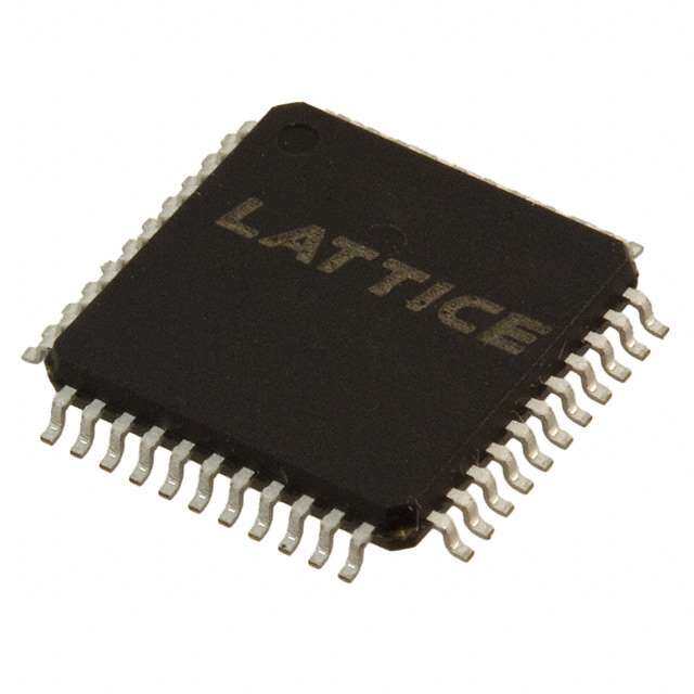
| 产品图片 |
|
| 产品型号 | XC2C128-7CPG132C |
| rohs | 无铅 / 符合限制有害物质指令(RoHS)规范要求 |
| 产品系列 | CoolRunner II |
| 产品目录页面 | |
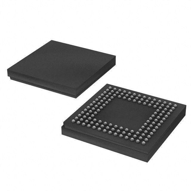
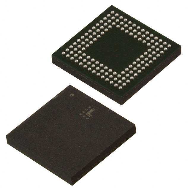
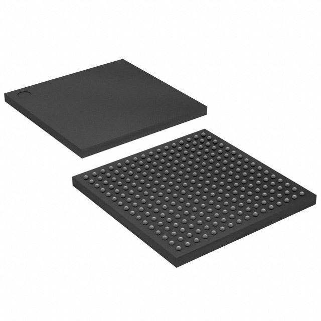
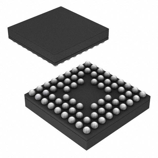
| 供应商器件封装 | 132-CSPBGA(8x8) |
| 其它名称 | 122-1396 |
| 包装 | 托盘 |
| 可编程类型 | 系统内可编程 |
| 安装类型 | 表面贴装 |
| 宏单元数 | 128 |
| 封装/外壳 | 132-TFBGA,CSPBGA |
| 工作温度 | 0°C ~ 70°C |
| 延迟时间tpd(1)最大值 | 7.0ns |
| 栅极数 | 3000 |
| 标准包装 | 360 |
| 电源电压-内部 | 1.7 V ~ 1.9 V |
| 逻辑元件/块数 | 8 |


- 商务部:美国ITC正式对集成电路等产品启动337调查
- 曝三星4nm工艺存在良率问题 高通将骁龙8 Gen1或转产台积电
- 太阳诱电将投资9.5亿元在常州建新厂生产MLCC 预计2023年完工
- 英特尔发布欧洲新工厂建设计划 深化IDM 2.0 战略
- 台积电先进制程称霸业界 有大客户加持明年业绩稳了
- 达到5530亿美元!SIA预计今年全球半导体销售额将创下新高
- 英特尔拟将自动驾驶子公司Mobileye上市 估值或超500亿美元
- 三星加码芯片和SET,合并消费电子和移动部门,撤换高东真等 CEO
- 三星电子宣布重大人事变动 还合并消费电子和移动部门
- 海关总署:前11个月进口集成电路产品价值2.52万亿元 增长14.8%

PDF Datasheet 数据手册内容提取
0 R XC2C128 CoolRunner-II CPLD DS093 (v3.2) March 8, 2007 Product Specification 0 0 Features Description • Optimized for 1.8V systems The CoolRunner-II 128-macrocell device is designed for - As fast as 5.7 ns pin-to-pin delays both high performance and low power applications. This - As low as 13 μA quiescent current lends power savings to high-end communication equipment and high speed to battery operated devices. Due to the low • Industry’s best 0.18 micron CMOS CPLD power stand-by and dynamic operation, overall system reli- - Optimized architecture for effective logic synthesis ability is improved - Multi-voltage I/O operation — 1.5V to 3.3V • Available in multiple package options This device consists of eight Function Blocks inter-con- - 100-pin VQFP with 80 user I/O nected by a low power Advanced Interconnect Matrix (AIM). The AIM feeds 40 true and complement inputs to each - 144-pin TQFP with 100 user I/O Function Block. The Function Blocks consist of a 40 by 56 - 132-ball CP (0.5mm) BGA with 100 user I/O P-term PLA and 16 macrocells which contain numerous - Pb-free available for all packages configuration bits that allow for combinational or registered • Advanced system features modes of operation. - Fastest in system programming Additionally, these registers can be globally reset or preset · 1.8V ISP using IEEE 1532 (JTAG) interface and configured as a D or T flip-flop or as a D latch. There - IEEE1149.1 JTAG Boundary Scan Test are also multiple clock signals, both global and local product - Optional Schmitt-trigger input (per pin) term types, configured on a per macrocell basis. Output pin - Unsurpassed low power management configurations include slew rate limit, bus hold, pull-up, · DataGATE enable (DGE) signal control open drain and programmable grounds. A Schmitt-trigger - Two separate I/O banks input is available on a per input pin basis. In addition to stor- - RealDigital 100% CMOS product term generation ing macrocell output states, the macrocell registers may be - Flexible clocking modes configured as direct input registers to store signals directly · Optional DualEDGE triggered registers from input pins. · Clock divider (divide by 2,4,6,8,10,12,14,16) · CoolCLOCK Clocking is available on a global or Function Block basis. - Global signal options with macrocell control Three global clocks are available for all Function Blocks as · Multiple global clocks with phase selection per a synchronous clock source. Macrocell registers can be macrocell individually configured to power up to the zero or one state. · Multiple global output enables A global set/reset control line is also available to asynchro- · Global set/reset nously set or reset selected registers during operation. - Advanced design security Additional local clock, synchronous clock-enable, asynchro- - Open-drain output option for Wired-OR and LED nous set/reset and output enable signals can be formed drive using product terms on a per-macrocell or per-Function - PLA architecture Block basis. · Superior pinout retention A DualEDGE flip-flop feature is also available on a per mac- · 100% product term routability across function rocell basis. This feature allows high performance synchro- block nous operation based on lower frequency clocking to help - Optional bus-hold, 3-state or weak pull-up on reduce the total power consumption of the device. selected I/O pins - Optional configurable grounds on unused I/Os Circuitry has also been included to divide one externally - Mixed I/O voltages compatible with 1.5V, 1.8V, supplied global clock (GCK2) by eight different selections. 2.5V, and 3.3V logic levels This yields divide by even and odd clock frequencies. · SSTL2-1, SSTL3-1, and HSTL-1 I/O compatibility The use of the clock divide (division by 2) and DualEDGE - Hot pluggable flip-flop gives the resultant CoolCLOCK feature. Refer to the CoolRunner™-II family data sheet for architec- DataGATE is a method to selectively disable inputs of the ture description. CPLD that are not of interest during certain points in time. © 2002-2007 Xilinx, Inc. All rights reserved. All Xilinx trademarks, registered trademarks, patents, and disclaimers are as listed at http://www.xilinx.com/legal.htm. All other trademarks and registered trademarks are the property of their respective owners. All specifications are subject to change without notice. DS093 (v3.2) March 8, 2007 www.xilinx.com 1 Product Specification
XC2C128 CoolRunner-II CPLD R By mapping a signal to the DataGATE function, lower power for I/O standard voltages. The LVTTL I/O standard is a gen- can be achieved due to reduction in signal switching. eral purpose EIA/JEDEC standard for 3.3V applications that use an LVTTL input buffer and Push-Pull output buffer. The Another feature that eases voltage translation is I/O bank- LVCMOSstandard is used in 3.3V, 2.5V, 1.8V applications. ing. Two I/O banks are available on the CoolRunner-II128 Both HSTL and SSTL make use of a V pin for JEDEC macrocell device that permit easy interfacing to 3.3V, 2.5V, REF compliance. CoolRunner-II CPLDs are also 1.5V I/O com- 1.8V, and 1.5V devices. patible with the use of Schmitt-trigger inputs. The CoolRunner-II 128 macrocell CPLD is I/O compatible with various JEDEC I/O standards (see Table1). This Table 1: I/O Standards for XC2C128(1) device is also 1.5V I/O compatible with the use of Board Schmitt-trigger inputs. IOSTANDARD Output Input Input Termination Attribute V V V Voltage V RealDigital Design Technology CCIO CCIO REF TT LVTTL 3.3 3.3 N/A N/A Xilinx CoolRunner-II CPLDs are fabricated on a 0.18 micron LVCMOS33 3.3 3.3 N/A N/A process technology which is derived from leading edge FPGA product development. CoolRunner-II CPLDs employ LVCMOS25 2.5 2.5 N/A N/A RealDigital technology, a design technique that makes use LVCMOS18 1.8 1.8 N/A N/A of CMOS technology in both the fabrication and design LVCMOS15(2) 1.5 1.5 N/A N/A methodology. RealDigital technology employs a cascade of HSTL_1 1.5 1.5 0.75 0.75 CMOS gates to implement sum of products instead of tradi- tional sense amplifier methodology. Due to this technology, SSTL2_1 2.5 2.5 1.25 1.25 Xilinx CoolRunner-II CPLDs achieve both high-perfor- SSTL3_1 3.3 3.3 1.5 1.5 mance and low power operation. (1) For information on assigning Vref pins, see XAPP399 (2) LVCMOS15 requires use of Schmitt-trigger inputs. Supported I/O Standards The CoolRunner-II 128 macrocell features LVCMOS, LVTTL, SSTL and HSTL I/O implementations. See Table1 40 ) A m 20 ( C C I 0 0 50 100 150 200 250 Frequency (MHz) DS093_041905 Figure 1: I vs Frequency CC Table 2: I vs Frequency (LVCMOS 1.8V T = 25°C)(1) CC A Frequency (MHz) 0 25 50 75 100 150 175 200 225 250 Typical I (mA) 0.019 3.97 7.95 11.92 15.89 23.83 27.80 31.93 35.73 39.70 CC Notes: 1. 16-bit up/down, Resetable binary counter (one counter per function block). 2 www.xilinx.com DS093 (v3.2) March 8, 2007 Product Specification
R XC2C128 CoolRunner-II CPLD Absolute Maximum Ratings Symbol Description Value Units V Supply voltage relative to ground –0.5 to 2.0 V CC V Supply voltage for output drivers –0.5 to 4.0 V CCIO V (2) JTAG input voltage limits –0.5 to 4.0 V JTAG V JTAG input supply voltage –0.5 to 4.0 V CCAUX V (1) Input voltage relative to ground –0.5 to 4.0 V IN V (1) Voltage applied to 3-state output –0.5 to 4.0 V TS T (3) Storage Temperature (ambient) –65 to +150 °C STG T Junction Temperature + 150 °C J Notes: 1. Maximum DC undershoot below GND must be limited to either 0.5V or 10 mA, whichever is easiest to achieve. During transitions, the device pins may undershoot to –2.0V or overshoot to +4.5V, provided this over or undershoot lasts less than 10ns and with the forcing current being limited to 200 mA. 2. Valid over commercial temperature range. 3. For soldering guidelines and thermal considerations, see the Device Packaging information on the Xilinx website. For Pb-free packages, see XAPP427. Recommended Operating Conditions Symbol Parameter Min Max Units V Supply voltage for internal logic Commercial T = 0°C to +70°C 1.7 1.9 V CC A and input buffers Industrial T = –40°C to +85°C 1.7 1.9 V A V Supply voltage for output drivers @ 3.3V operation 3.0 3.6 V CCIO Supply voltage for output drivers @ 2.5V operation 2.3 2.7 V Supply voltage for output drivers @ 1.8V operation 1.7 1.9 V Supply voltage for output drivers @ 1.5V operation 1.4 1.6 V V Supply voltage for JTAG programming 1.7 3.6 V CCAUX DC Electrical Characteristics (Over Recommended Operating Conditions) Symbol Parameter Test Conditions Typical Max. Units I Standby current Commercial V = 1.9V, V = 3.6V 30 120 μA CCSB CC CCIO I Standby current Industrial V = 1.9V, V = 3.6V 60 200 μA CCSB CC CCIO I (1) Dynamic current f = 1 MHz - 500 μA CC f = 50 MHz - 10 mA C JTAG input capacitance f = 1 MHz - 10 pF JTAG C Global clock input capacitance f = 1 MHz - 12 pF CLK C I/O capacitance f = 1 MHz - 10 pF IO I (2) Input leakage current V = 0V or V to 3.9V - +/–1 μA IL IN CCIO I (2) I/O High-Z leakage V = 0V or V to 3.9V - +/–1 μA IH IN CCIO Notes: 1. 16-bit up/down, Resetable binary counter (one counter per function block). 2. See Quality and Reliability section in CoolRunner-II family data sheet for details. DS093 (v3.2) March 8, 2007 www.xilinx.com 3 Product Specification
XC2C128 CoolRunner-II CPLD R LVCMOS and LVTTL 3.3V DC Voltage Specifications Symbol Parameter Test Conditions Min. Max. Units V Input source voltage 3.0 3.6 V CCIO V High level input voltage 2.0 3.9 V IH V Low level input voltage –0.3 0.8 V IL V High level output voltage I = –8 mA, V = 3V V – 0.4V - V OH OH CCIO CCIO I = –0.1 mA, V = 3V V – 0.2V - V OH CCIO CCIO V Low level output voltage I = 8 mA, V = 3V - 0.4 V OL OL CCIO I = 0.1 mA, V = 3V - 0.2 V OL CCIO LVCMOS 2.5V DC Voltage Specifications Symbol Parameter Test Conditions Min. Max. Units V Input source voltage 2.3 2.7 V CCIO V High level input voltage 1.7 V + 0.3(1) V IH CCIO V Low level input voltage –0.3 0.7 V IL V High level output voltage I = –8 mA, V = 2.3V V –0.4V - V OH OH CCIO CCIO I = –0.1 mA, V = 2.3V V – 0.2V - V OH CCIO CCIO V Low level output voltage I = 8 mA, V = 2.3V - 0.4 V OL OL CCIO I = 0.1 mA, V = 2.3V - 0.2 V OL CCIO (1) The V Max value represents the JEDEC specification for LVCMOS25. The CoolRunner-II input buffer can tolerate up to 3.9V without IH physical damage. LVCMOS 1.8V DC Voltage Specifications Symbol Parameter Test Conditions Min. Max. Units V Input source voltage 1.7 1.9 V CCIO V High level input voltage 0.65 x V V + 0.3(1) V IH CCIO CCIO V Low level input voltage –0.3 0.35 x V V IL CCIO V High level output voltage I = –8 mA, V = 1.7V V – 0.45 - V OH OH CCIO CCIO I = –0.1 mA, V = 1.7V V – 0.2 - V OH CCIO CCIO V Low level output voltage I = 8 mA, V = 1.7V - 0.45 V OL OL CCIO I = 0.1 mA, V = 1.7V - 0.2 V OL CCIO (1) The V Max value represents the JEDEC specification for LVCMOS18. The CoolRunner-II input buffer can tolerate up to 3.9V without IH physical damage. LVCMOS 1.5V DC Voltage Specifications(1) Symbol Parameter Test Conditions Min. Max. Units V Input source voltage 1.4 1.6 V CCIO V Input hysteresis threshold voltage 0.5 x V 0.8 x V V T+ CCIO CCIO V 0.2 x V 0.5 x V V T- CCIO CCIO V High level output voltage I = –8 mA, V = 1.4V V – 0.45 V OH OH CCIO CCIO I = –0.1 mA, V = 1.4V V – 0.2 V OH CCIO CCIO 4 www.xilinx.com DS093 (v3.2) March 8, 2007 Product Specification
R XC2C128 CoolRunner-II CPLD Symbol Parameter Test Conditions Min. Max. Units V Low level output voltage I = 8 mA, V = 1.4V 0.4 V OL OL CCIO I = 0.1 mA, V = 1.4V 0.2 V OL CCIO Notes: 1. Hysteresis used on 1.5V inputs. Schmitt Trigger Input DC Voltage Specifications Symbol Parameter Test Conditions Min. Max. Units V Input source voltage 1.4 3.9 V CCIO V Input hysteresis threshold voltage 0.5 x V 0.8 x V V T+ CCIO CCIO V 0.2 x V 0.5 x V V T- CCIO CCIO SSTL2-1 DC Voltage Specifications Symbol Parameter Test Conditions Min. Typ. Max. Units V Input source voltage 2.3 2.5 2.7 V CCIO V (1) Input reference voltage 1.15 1.25 1.35 V REF V (2) Termination voltage V – 0.04 1.25 V + 0.04 V TT REF REF V High level input voltage V + 0.18 - 3.9 V IH REF V Low level input voltage –0.3 - V – 0.18 V IL REF V High level output voltage I = –8 mA, V = 2.3V V – 0.62 - - V OH OH CCIO CCIO V Low level output voltage I = 8 mA, V = 2.3V - - 0.54 V OL OL CCIO Notes: 1. V should track the variations in V , also peak to peak ac noise on V may not exceed ±2% V REF CCIO REF REF. 2. V of transmitting device must track V of receiving devices. TT REF SSTL3-1 DC Voltage Specifications Symbol Parameter Test Conditions Min. Typ. Max. Units V Input source voltage 3.0 3.3 3.6 V CCIO V (1) Input reference voltage 1.3 1.5 1.7 V REF V (2) Termination voltage V – 0.05 1.5 V + 0.05 V TT REF REF V High level input voltage V + 0.2 - V + 0.3 V IH REF CCIO V Low level input voltage –0.3 - V – 0.2 V IL REF V High level output voltage I = –8 mA, V = 3V V – 1.1 - - V OH OH CCIO CCIO V Low level output voltage I = 8 mA, V = 3V - - 0.7 V OL OL CCIO Notes: 1. V should track the variations in V , also peak to peak ac noise on V may not exceed ±2% V REF CCIO REF REF. 2. V of transmitting device must track V of receiving devices. TT REF HSTL1 DC Voltage Specifications Symbol Parameter Test Conditions Min. Typ. Max. Units V Input source voltage 1.4 1.5 1.6 V CCIO V (1) Input reference voltage 0.68 0.75 0.90 V REF V (2) Termination voltage V x 0.5 V TT CCIO V High level input voltage V + 0.1 - 1.9 V IH REF V Low level input voltage –0.3 - V – 0.1 V IL REF DS093 (v3.2) March 8, 2007 www.xilinx.com 5 Product Specification
XC2C128 CoolRunner-II CPLD R Symbol Parameter Test Conditions Min. Typ. Max. Units V High level output voltage I = –8 mA, V = 1.7V V -0.4 - - V OH OH CCIO CCIO V Low level output voltage I = 8 mA, V = 1.7V - - 0.4 V OL OL CCIO Notes: 1. V should track the variations in V , also peak to peak ac noise on V may not exceed ±2% V REF CCIO REF REF. 2. V of transmitting device must track V of receiving devices. TT REF 6 www.xilinx.com DS093 (v3.2) March 8, 2007 Product Specification
R XC2C128 CoolRunner-II CPLD AC Electrical Characteristics Over Recommended Operating Conditions -6 -7 Symbol Parameter Min. Max. Min. Max. Units T Propagation delay single p-term - 5.7 - 7.0 ns PD1 T Propagation delay OR array - 6.0 - 7.5 ns PD2 T Direct input register set-up time 3.6 - 4.6 - ns SUD T Setup time fast (single p-term) 2.4 - 3.0 - ns SU1 T Setup time (OR array) 2.7 - 3.5 - ns SU2 T Direct input register hold time 0.0 - 0.0 - ns HD T Hold time (Or array or p-term) 0.0 - 0.0 - ns H T Clock to output - 4.2 - 5.4 ns CO F (1) Internal toggle rate - 450 - 300 MHz TOGGLE F (2) Maximum system frequency - 244 - 152 MHz SYSTEM1 F (2) Maximum system frequency - 227 - 141 MHz SYSTEM2 F (3) Maximum external frequency - 152 - 119 MHz EXT1 F (3) Maximum external frequency - 145 - 112 MHz EXT2 T Direct input register p-term clock setup time 2.5 - 3.1 - ns PSUD T P-term clock setup time (single p-term) 1.3 - 1.5 - ns PSU1 T P-term clock setup time (OR array) 1.6 - 2.0 - ns PSU2 T Direct input register p-term clock hold time 0.2 - 0.2 - ns PHD T P-term clock hold 0.7 - 1.0 - ns PH T P-term clock to output - 5.9 - 7.3 ns PCO T /T Global OE to output enable/disable - 5.9 - 7.5 ns OE OD T /T P-term OE to output enable/disable - 7.0 - 8.5 ns POE POD T /T Macrocell driven OE to output enable/disable - 7.7 - 9.9 ns MOE MOD T P-term set/reset to output valid - 6.6 - 8.1 ns PAO T Global set/reset to output valid - 5.0 - 7.6 ns AO T Register clock enable setup time 3.1 - 3.5 - ns SUEC T Register clock enable hold time 0.0 - 0.0 - ns HEC T Global clock pulse width High or Low 1.1 - 1.6 - ns CW T Asynchronous preset/reset pulse width (High or Low) 6.0 - 7.5 - ns APRPW T P-term pulse width High or Low 6.0 - 7.5 - ns PCW T Set-up before DataGATE latch assertion 0.0 - 0.0 - ns DGSU T Hold to DataGATE latch assertion 4.0 - 6.0 - ns DGH T DataGATE recovery to new data - 8.2 - 9.0 ns DGR T DataGATE low pulse width 3.0 - 4.0 - ns DGW T CDRST setup time before falling edge GCLK2 1.3 - 2.0 - ns CDRSU T Hold time CDRST after falling edge GCLK2 0.0 - 0.0 - ns CDRH T (4) Configuration time - 350 - 350 us CONFIG Notes: 1. F is the maximum clock frequency to which a T flip-flop can reliably toggle (see the CoolRunner-II family data sheet). TOGGLE 2. F is the internal operating frequency for a device with 16-bit resetable binary counter through one p-term per macrocell while SYSTEM1 F is through the OR array (one counter per function block). SYSTEM2 3. F (1/T +T ) is the maximum external frequency using one p-term while F is through the OR array. EXT1 SU1 CO EXT2 4. Typical configuration current during T is 10mA. CONFIG DS093 (v3.2) March 8, 2007 www.xilinx.com 7 Product Specification
XC2C128 CoolRunner-II CPLD R Internal Timing Parameters -6 -7 Symbol Parameter(1) Min. Max. Min. Max. Units Buffer Delays T Input buffer delay - 2.0 - 2.6 ns IN T Direct data register input delay - 3.7 - 5.3 ns DIN T Global Clock buffer delay - 1.5 - 2.1 ns GCK T Global set/reset buffer delay - 1.6 - 3.5 ns GSR T Global 3-state buffer delay - 2.1 - 3.0 ns GTS T Output buffer delay - 2.3 - 2.6 ns OUT T Output buffer enable/disable delay - 3.8 - 4.5 ns EN P-term Delays T Control term delay - 1.2 - 1.4 ns CT T Single P-term delay adder - 0.5 - 1.1 ns LOGI1 T Multiple P-term delay adder - 0.3 - 0.5 ns LOGI2 Macrocell Delay T Input to output valid - 0.9 - 0.7 ns PDI T Setup before clock (transparent latch) - 2.1 - 2.5 ns LDI T Setup before clock 1.4 - 1.4 - ns SUI T Hold after clock 0.0 - 0.0 - ns HI T Enable clock setup time 1.4 - 1.6 - ns ECSU T Enable clock hold time 0.0 - 0.0 - ns ECHO T Clock to output valid - 0.4 - 0.7 ns COI T Set/reset to output valid - 1.1 - 1.5 ns AOI T Clock doubler delay - 0.0 - 0.0 ns CDBL Feedback Delays T Feedback delay - 1.8 - 3.4 ns F T Macrocell to global OE delay - 2.0 - 2.6 ns OEM I/O Standard Time Adder Delays 1.5V CMOS T Hysteresis input adder - 3.0 - 4.0 ns HYS15 T Output adder - 0.8 - 1.0 ns OUT15 T Output slew rate adder - 4.0 - 4.0 ns SLEW15 I/O Standard Time Adder Delays 1.8V CMOS T Hysteresis input adder - 2.0 - 4.0 ns HYS18 T Input adder - 0 - 0 ns IN18 T Output adder - 0.0 - 0.0 ns OUT18 T Output slew rate adder - 2.5 - 4.0 ns SLEW18 8 www.xilinx.com DS093 (v3.2) March 8, 2007 Product Specification
R XC2C128 CoolRunner-II CPLD Internal Timing Parameters (Continued) -6 -7 Symbol Parameter(1) Min. Max. Min. Max. Units I/O Standard Time Adder Delays 2.5V CMOS T Standard input adder - 0.6 - 0.7 ns IN25 T Hysteresis input adder - 1.5 - 3.0 ns HYS25 T Output adder - 0.8 - 0.9 ns OUT25 T Output slew rate adder - 3.0 - 4.0 ns SLEW25 I/O Standard Time Adder Delays 3.3V CMOS/TTL T Standard input adder - 0.5 - 0.6 ns IN33 T Hysteresis input adder - 1.2 - 3.0 ns HYS33 T Output adder - 1.2 - 1.4 ns OUT33 T Output slew rate adder - 3.0 - 4.0 ns SLEW33 I/O Standard Time Adder Delays HSTL, SSTL SSTL2-1 Input adder to T , T , T , T , - 0.8 - 2.5 ns IN DIN GCK GSR T GTS Output adder to T - 0.5 - 0.5 ns OUT SSTL3-1 Input adder to T , T , T , T , - 0.8 - 2.5 ns IN DIN GCK GSR T GTS Output adder to T - 0.5 - 0.5 ns OUT HSTL-1 Input adder to T , T , T , T , - 2.0 - 2.5 ns IN DIN GCK GSR T GTS Output adder to T - 0.0 - 0.0 ns OUT Notes: 1. 1.5 ns input pin signal rise/fall. Switching Characteristics Switching Test Conditions VCC = VCCIO = 1.8V, 25oC VCC 5.0 R1 4.8 Device Under Test Test Point 4.6 R2 CL s) n (2 4.4 D P T Output Type R1 R2 CL 4.2 LVTTL33 268Ω 235Ω 35 pF LVCMOS33 275Ω 275Ω 35 pF 4.0 LVCMOS25 188Ω 188Ω 35 pF 1 2 4 8 16 LVCMOS18 112.5Ω 112.5Ω 35 pF Number of Outputs Switching LVCMOS15 150Ω 150Ω 35 pF Notes: DS093_02_050103 1. CL includes test fixtures and probe capacitance. 2. 1.5 nsec maximum rise/fall times on inputs. Figure 2: Derating Curve for T PD DS092_03_092302 Figure 3: AC Load Circuits DS093 (v3.2) March 8, 2007 www.xilinx.com 9 Product Specification
XC2C128 CoolRunner-II CPLD R Typical I/V Output Curves The I/V curve illustrates the nominal amount of current that an I/O can source/sink at different voltage levels. 3.3V 60 50 A) m nt 40 2.5V e urr 1.8V C ut Iol p 30 ut O O ( I 20 1.5V 10 0 0 .5 1.0 1.5 2.0 2.5 3.0 3.5 VO (Output Volts) XC128_IV_all_050703 Figure 4: Typical I/V Curves for XC2C128 1P1 in Descriptions Pin Descriptions (Continued) Function Macro- I/O Function Macro- I/O Block cell VQ100 CP132 TQ144 Bank Block cell VQ100 CP132 TQ144 Bank 1 1 13 G1 17 2 2 1 - G2 19 1 1 2 - F1 16 2 2 2 14 G3 21 1 1 3 12 F2 15 2 2 3 15 H1 22 1 1 4 11 F3 14 2 2 4 16 H2 23 1 1 5 10 E1 13 2 2 5 17 H3 24 1 1 6 9 E2 12 2 2 6 18 J1 25 1 1 7 - - - - 2 7 - - - - 1 8 - - - - 2 8 - - - - 1 9 - - - - 2 9 - - - - 1 10 - - - - 2 10 - - - - 1 11 8 E3 11 2 2 11 19 J2 26 1 1 12 7 D1 10 2 2 12 - K1 28 1 1 13 6 D2 9 2 2(GCK0) 13 22 K3 30 1 1 14 - C1 7 2 2(GCK1) 14 23 L2 32 1 1(GTS1) 15 4 C2 6 2 2(CDRST) 15 24 M2 35 1 1(GTS0) 16 3 C3 5 2 2(GCK2) 16 27 N2 38 1 10 www.xilinx.com DS093 (v3.2) March 8, 2007 Product Specification
R XC2C128 CoolRunner-II CPLD Pin Descriptions (Continued) Pin Descriptions (Continued) Function Macro- I/O Function Macro- I/O Block cell VQ100 CP132 TQ144 Bank Block cell VQ100 CP132 TQ144 Bank 3 1 - B1 4 2 5 1 65 G13 94 2 3(GTS3) 2 2 B2 3 2 5 2 66 G12 95 2 3(GTS2) 3 1 A1 2 2 5 3 67 F14 96 2 3(GSR) 4 99 A3 143 2 5 4 - F13 97 2 3 5 97 B4 140 2 5 5 68 F12 98 2 3 6 96 A4 138 2 5 6 - E13 100 2 3 7 95 C5 136 2 5 7 70 E12 101 2 3 8 - - - - 5 8 - - - - 3 9 - - - - 5 9 - - - - 3 10 - - - - 5 10 - - - - 3 11 94 B5 134 2 5 11 71 D14 102 2 3 12 A5 133 2 5 12 72 D13 103 2 3 13 93 C6 132 2 5 13 73 D12 104 2 3 14 92 B6 131 2 5 14 74 C14 105 2 3 15 91 A6 130 2 5 15 76 B13 110 2 3 16 90 C7 129 2 5 16 - A13 111 2 4(DGE) 1 28 P2 39 1 6 1 64 H12 92 1 4 2 - M3 40 1 6 2 63 H13 91 1 4 3 - N3 41 1 6 3 61 J13 88 1 4 4 29 P3 43 1 6 4 60 J12 87 1 4 5 30 M4 45 1 6 5 59 K14 86 1 4 6 32 M5 49 1 6 6 58 K13 85 1 4 7 33 N5 50 1 6 7 - - - - 4 8 - - - - 6 8 - - - - 4 9 - - - - 6 9 - - - - 4 10 - - - - 6 10 - - - - 4 11 34 P5 51 1 6 11 - L14 83 1 4 12 35 M6 52 1 6 12 56 L13 82 1 4 13 36 N6 53 1 6 13 - L12 81 1 4 14 37 P6 54 1 6 14 55 M14 80 1 4 15 39 N7 56 1 6 15 - M13 79 1 4 16 40 M7 57 1 6 16 54 M12 78 1 DS093 (v3.2) March 8, 2007 www.xilinx.com 11 Product Specification
XC2C128 CoolRunner-II CPLD R Pin Descriptions (Continued) Pin Descriptions (Continued) Function Macro- I/O Function Macro- I/O Block cell VQ100 CP132 TQ144 Bank Block cell VQ100 CP132 TQ144 Bank 7 1 77 C12 112 2 8 1 - N14 77 1 7 2 78 B12 113 2 8 2 53 N13 76 1 7 3 - A12 115 2 8 3 52 P14 74 1 7 4 79 C11 116 2 8 4 50 P12 71 1 7 5 80 B11 117 2 8 5 - M11 70 1 7 6 81 A11 118 2 8 6 49 N11 69 1 7 7 - C10 119 2 8 7 - - - - 7 8 - - - - 8 8 - - - - 7 9 - - - - 8 9 - - - - 7 10 - - - - 8 10 - - - - 7 11 82 A10 120 2 8 11 - P11 68 1 7 12 - C9 121 2 8 12 46 P10 64 1 7 13 85 A8 124 2 8 13 44 P9 61 1 7 14 86 B8 125 2 8 14 43 M8 60 1 7 15 87 C8 126 2 8 15 42 N8 59 1 7 16 89 B7 128 2 8 16 41 P8 58 1 Notes: 1. GTS = global output enable, GSR = global reset/set, GCK = global clock, CDRST = clock divide reset, DGE = DataGATE enable. 2. GCK, GSR, and GTS pins can also be used for general purpose I/O. 12 www.xilinx.com DS093 (v3.2) March 8, 2007 Product Specification
R XC2C128 CoolRunner-II CPLD XC2C128 JTAG, Power/Ground, No Connect Pins and Total User I/O Pin Type VQ100(1) CP132(1) TQ144(1) TCK 48 M10 67 TDI 45 M9 63 TDO 83 B9 122 TMS 47 N10 65 V (JTAG supply voltage) 5 D3 8 CCAUX Power internal (V ) 26, 57 P1, K12, A2 1, 37, 84 CC Power Bank 1 I/O (V ) 20, 38, 51 J3, P7, G14, P13 27, 55, 73, 93 CCIO1 Power Bank 2 I/O (V ) 88, 98 A14, C4, A7 109, 127, 141 CCIO2 Ground 21, 25, 31, 62, 69, 75, K2, N1, P4, N9, N12, J14, 29, 36, 47, 62, 72, 89, 90, 84, 100 H14, E14, B14, A9, B3 99, 108, 123, 144 No connects - L1, L3, M1, N4, C13, B10 18, 20, 31, 33, 34, 42, 44, 46, 48, 66, 75, 106, 107, 114, 135, 137, 139, 142 Total user I/O (including dual function 80 100 100 pins) Notes: 1. Pin compatible with all larger and smaller densities except where I/O banking is used. Ordering Information Comm. Pin/Ball θ θ Package Body (C) JA JC Part Number Spacing (C/Watt) (C/Watt) Package Type Dimensions I/O Ind. (I)(1) XC2C128-6VQ100C 0.5mm 47.5 12.5 Very Thin Quad Flat 14mm x 14mm 80 C Pack XC2C128-7VQ100C 0.5mm 47.5 12.5 Very Thin Quad Flat 14mm x 14mm 80 C Pack XC2C128-6CP132C 0.5mm 72.4 15.7 Chip Scale Package 8mm x 8mm 100 C XC2C128-7CP132C 0.5mm 72.4 15.7 Chip Scale Package 8mm x 8mm 100 C XC2C128-6TQ144C 0.5mm 46.1 7.9 Thin Quad Flat Pack 20mm x 20mm 100 C XC2C128-7TQ144C 0.5mm 46.1 7.9 Thin Quad Flat Pack 20mm x 20mm 100 C XC2C128-6VQG100C 0.5mm 47.5 12.5 Very Thin Quad Flat 14mm x 14mm 80 C Pack; Pb-free XC2C128-7VQG100C 0.5mm 47.5 12.5 Very Thin Quad Flat 14mm x 14mm 80 C Pack; Pb-free XC2C128-6CPG132C 0.5mm 72.4 15.7 Chip Scale 8mm x 8mm 100 C Package; Pb-free XC2C128-7CPG132C 0.5mm 72.4 15.7 Chip Scale 8mm x 8mm 100 C Package; Pb-free XC2C128-6TQG144C 0.5mm 46.1 7.9 Thin Quad Flat 20mm x 20mm 100 C Pack; Pb-free XC2C128-7TQG144C 0.5mm 46.1 7.9 Thin Quad Flat 20mm x 20mm 100 C Pack; Pb-free XC2C128-7VQ100I 0.5mm 47.5 12.5 Very Thin Quad Flat 14mm x 14mm 80 I Pack DS093 (v3.2) March 8, 2007 www.xilinx.com 13 Product Specification
XC2C128 CoolRunner-II CPLD R Comm. Pin/Ball θ θ Package Body (C) JA JC Part Number Spacing (C/Watt) (C/Watt) Package Type Dimensions I/O Ind. (I)(1) XC2C128-7CP132I 0.5mm 72.4 15.7 Chip Scale Package 8mm x 8mm 100 I XC2C128-7TQ144I 0.5mm 46.1 7.9 Thin Quad Flat Pack 20mm x 20mm 100 I XC2C128-7VQG100I 0.5mm 47.5 12.5 Very Thin Quad Flat 14mm x 14mm 80 I Pack; Pb-free XC2C128-7CPG132I 0.5mm 72.4 15.7 Chip Scale 8mm x 8mm 100 I Package; Pb-free XC2C128-7TQG144I 0.5mm 46.1 7.9 Thin Quad Flat 20mm x 20mm 100 I Pack; Pb-free Notes: C = Commercial (T A = 0° C to +70° C); I = Industrial (T A = –40° C to +85° C). Standard Example: X C 2 C 1 28 - 6 TQ 144 C Pb-Free Example: X C 2 C 1 28 -6 TQ G 144 C Device Device Speed Grade Speed Grade Package Type Package Type Number of Pins Pb-Free Temperature Range Number of Pins Temperature Range Device Part Marking R Device Type XC2Cxxx Package TQ144 This line not related to device part number Speed 7C Operating Range Part Marking for all non chip scale packages Figure 5: Sample Package with Part Marking Note: Due to the small size of chip scale packages, the complete ordering part number cannot be included on the package marking. Part marking on chip scale packages by line are: • Line 1 = X (Xilinx logo) then truncated part number • Line 4 = Package code, speed, operating temperature, • Line 2 = Not related to device part number three digits not related to device part number. Package codes: C5 = CP132, C6 = CPG132. • Line 3 = Not related to device part number 14 www.xilinx.com DS093 (v3.2) March 8, 2007 Product Specification
R XC2C128 CoolRunner-II CPLD O2 O2 ND(3)OCCIOOOOOOOOOCCIOOONDDOOOOOOOO GI/VI/I/I/I/I/I/I/I/I/VI/I/I/GTI/I/I/I/I/I/I/ 0987654321098765432109876 I/O(1) 11099999999998888888888777775 GND I/O(1) 2 74 I/O I/O(1) 3 73 I/O I/O(1) 4 72 I/O VAUX 5 71 I/O I/O 6 70 I/O I/O 7 69 GND I/O 8 68 I/O I/O 9 67 I/O I/O 10 66 I/O I/O 11 VQ100 65 I/O I/O 12 Top View 64 I/O I/O 13 63 I/O I/O 14 62 GND I/O 15 61 I/O I/O 16 60 I/O I/O 17 59 I/O I/O 18 58 I/O I/O 19 57 VCC VCCIO1 20 56 I/O GND 21 55 I/O I/O(2) 22 54 I/O I/O(2) 23 53 I/O I/O(4) 24 52 I/O GND 25 51 VCCIO1 6789012345678901234567890 2222333333333344444444445 VCC(2)I/O(5)I/OI/OI/OGNDI/OI/OI/OI/OI/OI/OCCIO1I/OI/OI/OI/OI/OI/OTDII/OTMSTCKI/OI/O V (1) - Global Output Enable (2) - Global Clock (3) - Global Set/Reset (4) - Clock Divide Reset (5) - Data Gate Figure 6: VQ100 Very Thin Quad Flat Pack DS093 (v3.2) March 8, 2007 www.xilinx.com 15 Product Specification
XC2C128 CoolRunner-II CPLD R 0 1 2 3 4 1 2 3 4 5 6 7 8 9 1 1 1 1 1 P VCC I/O(5) I/O GND I/O I/O VCCIO1 I/O I/O I/O I/O I/O VCCIO1 I/O N GND I/O(2) I/O NC I/O I/O I/O I/O GND TMS I/O GND I/O I/O M NC I/O(4) I/O I/O I/O I/O I/O I/O TDI TCK I/O I/O I/O I/O L NC I/O(2) NC I/O I/O I/O K I/O GND I/O(2) VCC I/O I/O J I/O I/O VCCIO1 I/O I/O GND H I/O I/O I/O I/O I/O GND CP132 G I/O I/O I/O Bottom View I/O I/O VCCIO1 F I/O I/O I/O I/O I/O I/O E I/O I/O I/O I/O I/O GND D I/O I/O VAUX I/O I/O I/O C I/O I/O(1) I/O(1) VCCIO2 I/O I/O I/O I/O I/O I/O I/O I/O NC I/O B I/O I/O(1) GND I/O I/O I/O I/O I/O TDO NC I/O I/O I/O GND A I/O(1) VCC I/O(3) I/O I/O I/O VCCIO2 I/O GND I/O I/O I/O I/O VCCIO2 (1) - Global Output Enable (2) - Global Clock (3) - Global Set/Reset (4) - Clock Divide Reset (5) - DataGATE Enable Figure 7: CP132 Chip Scale Package 16 www.xilinx.com DS093 (v3.2) March 8, 2007 Product Specification
R XC2C128 CoolRunner-II CPLD 2 2 2 O O O ND(3)OCCCIOCOCOCOOOOOOOCCIOOONDDOOOOOOOOCOOOOCCI GI/NVI/NI/NI/NI/I/I/I/I/I/I/VI/I/I/GTI/I/I/I/I/I/I/NI/I/I/I/V 432109876543210987654321098765432109 I/VOC(1C) 12 141414141413131313131313131313121212121212121212121111111111111111111110108 GND I/O(1) 3 107 NC I/O 4 106 NC I/O(1) 5 105 I/O I/O(1) 6 104 I/O I/O 7 103 I/O VAUX 8 102 I/O I/O 9 101 I/O I/O 10 100 I/O I/O 11 99 GND I/O 12 98 I/O I/O 13 97 I/O I/O 14 96 I/O I/O 15 95 I/O I/O 16 94 I/O I/O 17 93 VCCIO1 NC 18 TQ144 92 I/O I/O 19 91 I/O NC 20 Top View 90 GND I/O 21 89 GND I/O 22 88 I/O I/O 23 87 I/O I/O 24 86 I/O I/O 25 85 I/O I/O 26 84 VCC VCCIO1 27 83 I/O I/O 28 82 I/O GND 29 81 I/O I/O(2) 30 80 I/O NC 31 79 I/O I/O(2) 32 78 I/O NC 33 77 I/O NC 34 76 I/O I/O(4) 35 75 NC GND 36 74 I/O 73 VCCIO1 789012345678901234567890123456789012 333444444444455555555556666666666777 VCC(2)I/O(5)I/OI/OI/ONCI/ONCI/ONCGNDNCI/OI/OI/OI/OI/OI/OCCIO1I/OI/OI/OI/OI/OI/OGNDTDII/OTMSNCTCKI/OI/OI/OI/OGND V (1) - Global Output Enable (2) - Global Clock (3) - Global Set/Reset (4) - Clock Divide Reset (5) - DataGATE Enable Figure 8: TQ144 Thin Quad Flat Pack Warranty Disclaimer THESE PRODUCTS ARE SUBJECT TO THE TERMS OF THE XILINX LIMITED WARRANTY WHICH CAN BE VIEWED AT http://www.xilinx.com/warranty.htm. THIS LIMITED WARRANTY DOES NOT EXTEND TO ANY USE OF THE PRODUCTS IN AN APPLICATION OR ENVIRONMENT THAT IS NOT WITHIN THE SPECIFICATIONS STATED ON THE THEN-CURRENT XILINX DATA SHEET FOR THE PRODUCTS. PRODUCTS ARE NOT DESIGNED TO BE FAIL-SAFE AND ARE NOT WARRANTED FOR USE IN APPLICATIONS THAT POSE A RISK OF PHYSICAL HARM OR LOSS OF LIFE. USE OF PRODUCTS IN SUCH APPLICATIONS IS FULLY AT THE RISK OF CUSTOMER SUBJECT TO APPLICABLE LAWS AND REGULATIONS. DS093 (v3.2) March 8, 2007 www.xilinx.com 17 Product Specification
XC2C128 CoolRunner-II CPLD R Additional Information Additional information is available for the following CoolRunner-II topics: • XAPP784: Bulletproof CPLD Design Practices To access these and all application notes with their associ- • XAPP375: Timing Model ated reference designs, click the following link and scroll down the page until you find the document you want: • XAPP376: Logic Engine • XAPP378: Advanced Features CoolRunner-II Data Sheets and Application Notes • XAPP382: I/O Characteristics Device Packages • XAPP389: Powering CoolRunner-II • XAPP399: Assigning VREF Pins Revision History The following table shows the revision history for this document. Date Version Revision 10/01/02 1.0 Initial Xilinx release. 5/19/03 2.0 Added bin 6, 7 characterization data. 8/25/03 2.1 Edit Package diagram, other minor formatting edits. 01/26/04 2.2 Update links. 03/01/04 2.3 Fixed cropping on Figure 6. 7/30/04 2.4 Added Pb-free documentation. 10/01/04 2.5 Add Asynchronous Preset/Reset Pulse Width specification to AC Electrical Characteristics. 01/30/05 2.6 Change to I MAX for Commercial and Industrial. CCSB 03/07/05 2.7 Delete -4 speed grade. Modifications to Table 1, IOSTANDARDs. 04/21/05 2.8 Recharacterization of AC Specifications 06/28/05 2.9 Move to Product Specification. 03/20/06 3.0 Add Warranty Disclaimer. Add note to Pin Descriptions that GCK, GSR, and GTS pins can also be used for general purpose I/O. Replaced Figure 3 with a higher resolution graphic. 02/15/07 3.1 Corrections to timing parameters t , t , t , t , t and f for -6 speed grade. F CT DIN GTS OEM TOGGLE Corrections to t , t , t , t , t , t , t , F , and F for the -7 speed grade. DIN GCK EN SUI ECSU F OEM EXT1 EXT2 Values now match the software. There were no changes to silicon or characterization. Change to V specification for 2.5V and 1.8V LVCMOS. IH 03/08/07 3.2 Fixed typo in note for V for LVCMOS18; removed note for V for LVCMOS33. IL IL 18 www.xilinx.com DS093 (v3.2) March 8, 2007 Product Specification