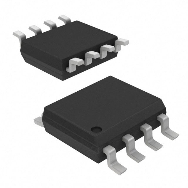
ICGOO在线商城 > 集成电路(IC) > 数据采集 - 数字电位器 > X9511WSZ
- 型号: X9511WSZ
- 制造商: Intersil
- 库位|库存: xxxx|xxxx
- 要求:
| 数量阶梯 | 香港交货 | 国内含税 |
| +xxxx | $xxxx | ¥xxxx |
查看当月历史价格
查看今年历史价格
X9511WSZ产品简介:
ICGOO电子元器件商城为您提供X9511WSZ由Intersil设计生产,在icgoo商城现货销售,并且可以通过原厂、代理商等渠道进行代购。 X9511WSZ价格参考。IntersilX9511WSZ封装/规格:数据采集 - 数字电位器, Digital Potentiometer 10k Ohm 1 Circuit 32 Taps Pushbutton Interface 8-SOIC。您可以下载X9511WSZ参考资料、Datasheet数据手册功能说明书,资料中有X9511WSZ 详细功能的应用电路图电压和使用方法及教程。
Renesas Electronics America Inc. 生产的型号为 X9511WSZ 的数字电位器,属于数据采集类元件。其应用场景主要包括以下几方面:

 1. 音频设备
   - 在音频设备中,X9511WSZ 可用于音量控制、平衡调整和增益调节。通过数字接口实现精确的电阻值调节,适用于音响系统、耳机放大器和其他音频处理设备。

 2. 工业控制
   - 在工业自动化领域,数字电位器可用于调节传感器信号增益、校准模拟信号输出或控制电机速度。例如,在 PLC(可编程逻辑控制器)或数据采集系统中,X9511WSZ 可作为可调电阻来优化信号处理性能。

 3. 医疗设备
   - 医疗仪器如心率监测仪、血压计或超声波设备需要高精度的信号调节。X9511WSZ 能够提供稳定的电阻调节功能,用于信号放大器的增益控制或滤波器的频率调节。

 4. 通信设备
   - 在通信领域,数字电位器可用于调节射频电路中的匹配网络或滤波器参数。例如,在无线通信模块中,X9511WSZ 可帮助优化信号强度和减少干扰。

 5. 消费电子
   - 消费电子产品如智能家居设备、便携式仪器等,需要灵活的电阻调节功能。X9511WSZ 可用于亮度调节、温度控制或其他需要动态调整的场景。

 6. 汽车电子
   - 在汽车电子系统中,数字电位器可用于调节车内音响系统的音量、均衡器设置或仪表盘的背光亮度。此外,它还可用于传感器信号调理或控制模块的校准。

 特性与优势
- 高分辨率:支持精细的电阻调节,满足多种应用需求。
- 低功耗:适合电池供电设备,延长工作时间。
- 小型化设计:易于集成到紧凑型电路板中。
- 稳定性强:在宽温范围内保持良好的性能一致性。

综上所述,X9511WSZ 数字电位器凭借其灵活性和高精度,广泛应用于需要动态电阻调节的各种领域,特别是在对信号处理和系统校准要求较高的场景中表现出色。
| 参数 | 数值 |
| 产品目录 | 集成电路 (IC)半导体 |
| 描述 | IC POT DGTL SGL PB CTRL 8-SOIC数字电位计 IC PUSHPOT 32 TAP DIG CONTROL E2POT 10KOHM |
| 产品分类 | |
| 品牌 | Intersil |
| 产品手册 | |
| 产品图片 |
|
| rohs | 符合RoHS无铅 / 符合限制有害物质指令(RoHS)规范要求 |
| 产品系列 | 数字电位计 IC,Intersil X9511WSZXDCP™ |
| 数据手册 | |
| 产品型号 | X9511WSZ |
| PCN组件/产地 | |
| POT数量 | Single |
| 产品目录页面 | |
| 产品种类 | 数字电位计 IC |
| 供应商器件封装 | 8-SOIC |
| 包装 | 管件 |
| 商标 | Intersil |
| 存储器类型 | 非易失 |
| 安装类型 | 表面贴装 |
| 安装风格 | SMD/SMT |
| 容差 | 20 % |
| 封装 | Tube |
| 封装/外壳 | 8-SOIC(0.154",3.90mm 宽) |
| 封装/箱体 | SOIC-8 |
| 工作温度 | 0°C ~ 70°C |
| 工作电源电压 | 5 V |
| 工厂包装数量 | 100 |
| 弧刷存储器 | Non Volatile |
| 抽头 | 32 |
| 接口 | 2 线按钮 |
| 数字接口 | Push Button |
| 最大工作温度 | + 70 C |
| 最小工作温度 | 0 C |
| 标准包装 | 100 |
| 每POT分接头 | 32 |
| 温度系数 | 300 PPM / C |
| 电压-电源 | 4.5 V ~ 5.5 V |
| 电源电压-最大 | 5.5 V |
| 电源电压-最小 | 4.5 V |
| 电源电流 | 1 mA |
| 电路数 | 1 |
| 电阻 | 10 kOhms |
| 电阻(Ω) | 10k |
| 系列 | X9511 |




- 商务部:美国ITC正式对集成电路等产品启动337调查
- 曝三星4nm工艺存在良率问题 高通将骁龙8 Gen1或转产台积电
- 太阳诱电将投资9.5亿元在常州建新厂生产MLCC 预计2023年完工
- 英特尔发布欧洲新工厂建设计划 深化IDM 2.0 战略
- 台积电先进制程称霸业界 有大客户加持明年业绩稳了
- 达到5530亿美元!SIA预计今年全球半导体销售额将创下新高
- 英特尔拟将自动驾驶子公司Mobileye上市 估值或超500亿美元
- 三星加码芯片和SET,合并消费电子和移动部门,撤换高东真等 CEO
- 三星电子宣布重大人事变动 还合并消费电子和移动部门
- 海关总署:前11个月进口集成电路产品价值2.52万亿元 增长14.8%




PDF Datasheet 数据手册内容提取
DATASHEET X9511 FN8205 Single Push Button Controlled Potentiometer (XDCP™) Linear, 32 Taps, Push Rev 3.00 Button Controlled, Terminal Voltage ±5V February 2, 2007 FEATURES DESCRIPTION • Push button controlled The Intersil X9511 is a push button controlled potenti- • Low power CMOS ometer that is ideal for push button controlled resis- —Active current, 3mA max tance trimming. —Standby current, 100µA typical The X9511 is a resistor array composed of 31 resistive • 31 resistive elements elements. Between each element and at either end —Temperature compensated are tap points accessible to the wiper element. The —20% end to end resistance range position of the wiper element is controlled by the PU —-5V to +5V range and PD inputs. The position of the wiper can be auto- • 32 wiper tap points 2 matically stored in E memory and then be recalled —Wiper positioned via two push button inputs upon a subsequent power-on operation. —Slow and fast scan modes ® —AUTOSTORE option The resolution of the X9511 is equal to the maximum —Manual store option resistance value divided by 31. As an example, for the —Wiper position stored in nonvolatile memory X9511W (10k) each tap point represents 323. and recalled on power-up All Intersil nonvolatile products are designed and • 100 year wiper position data retention tested for applications requiring extended endurance • X9511W = 10k • Packages and data retention. —8 Ld PDIP —8 Ld SOIC • Pb-free plus anneal available (RoHS compliant) ORDERING INFORMATION RTOTAL TEMPERATURE PART NUMBER PART MARKING (k) RANGE (°C) PACKAGE PKG. DWG. # X9511WP X9511WP 10 0 to +70 8 Ld PDIP MDP0031 X9511WPZ (Note) X9511WP Z 0 to +70 8 Ld PDIP*** (Pb-free) MDP0031 X9511WPI X9511WP I -40 to +85 8 Ld PDIP MDP0031 X9511WPIZ (Note) X9511WP Z I -40 to +85 8 Ld PDIP*** (Pb-free) MDP0031 X9511WS** X9511W 0 to +70 8 Ld SOIC MDP0027 X9511WSZ*, **(Note) X9511W Z 0 to +70 8 Ld SOIC (Pb-free) MDP0027 X9511WSI*, ** X9511W I -40 to +85 8 Ld SOIC MDP0027 X9511WSIZ*, ** (Note) X9511W Z I -40 to +85 8 Ld SOIC (Pb-free) MDP0027 NOTE: Intersil Pb-free plus anneal products employ special Pb-free material sets; molding compounds/die attach materials and 100% matte tin plate termination finish, which are RoHS compliant and compatible with both SnPb and Pb-free soldering operations. Intersil Pb-free products are MSL classified at Pb-free peak reflow temperatures that meet or exceed the Pb-free requirements of IPC/JEDEC J STD-020. *Add "T1" suffix for tape and reel. **Add "T2" suffix for tape and reel. ***Pb-free PDIPs can be used for through hole wave solder processing only. They are not intended for use in Reflow solder processing applications. FN8205 Rev 3.00 Page 1 of 9 February 2, 2007
X9511 BLOCK DIAGRAM PU 5-BIT 31 VH UP/DOWN PD COUNTER 30 29 5-BIT 28 EEPROM ONE MEMORY OF THIRTY-TWO TRANSFER RESISTOR DECODER GATES ARRAY 2 STORE AND RECALL 1 ASE CONTROL CIRCUITRY 0 VL VW FN8205 Rev 3.00 Page 2 of 9 February 2, 2007
X9511 PIN DESCRIPTIONS PIN NAMES SYMBOL DESCRIPTION V /R and V /R H H L L The high (V /R ) and low (V /R ) terminals of the VH/RH High Terminal H H L L X9511 are equivalent to the fixed terminals of a mechan- V /R Wiper Terminal W W ical potentiometer. The minimum voltage is -5V and the V /R Low Terminal L L maximum is +5V. It should be noted that the terminology V Ground of V /R and V /R are in reference to the relative posi- SS L L H H tion of the terminal in relation to wiper movement direc- VCC Supply Voltage tion selected by the PU and PD inputs, and not the PU Push Up Input voltage potential on the terminal. PD Push Down Input PU ASE AUTOSTORE Enable Input The debounced PU input is for incrementing the wiper DEVICE OPERATION position. An on-chip pull-up holds the PU input HIGH. A switch closure to ground or a LOW logic level will, after a There are three sections of the X9511: the input control, debounce time, move the wiper to the next adjacent counter and decode section; the EEPROM memory; and higher tap position. the resistor array. The input control section operates just like an up/down counter. The output of this counter is PD decoded to turn on a single electronic switch, connecting The debounced PD input is for decrementing the wiper a point on the resistor array to the wiper output. Under the position. An on-chip pull-up holds the PD input HIGH. A proper conditions the contents of the counter can be switch closure to ground or a LOW logic level will, after a stored in EEPROM memory and retained for future use. debounce time, move the wiper to the next adjacent The resistor array is comprised of 31 individual resistors lower tap position. connected in series. At either end of the array and between each resistor is an electronic switch that trans- ASE fers the potential at that point to the wiper. The debounced ASE (AUTOSTORE enable) pin can be The X9511 is designed to interface directly to two push in one of two states: button switches for effectively moving the wiper up or down. The PU and PD inputs increment or decrement a V - AUTOSTORE is enabled. When V powers IL CC 5-bit counter respectively. The output of this counter is down, an automatic store cycle takes place. decoded to select one of the thirty-two wiper positions VIH - AUTOSTORE is disabled. A LOW to HIGH will initi- along the resistive array. The wiper increment input, PU ate a manual store operation. This is for the user who and the wiper decrement input, PD are both connected wishes to connect a push button switch to this pin. For to an internal pull-up so that they normally remain HIGH. every valid push, the X9511 will store the current wiper When pulled LOW by an external push button switch or position to the EEPROM. a logic LOW level input, the wiper will be switched to the next adjacent tap position. PIN CONFIGURATION Internal debounce circuitry prevents inadvertent switch- DIP/SOIC ing of the wiper position if PU or PD remain LOW for less than 40ms, typical. Each of the buttons can be pushed PU 1 8 VCC either once for a single increment/decrement or continu- PD 2 7 ASE ously for a multiple increments/decrements. The number X9511 VH 3 6 VL of increments/decrements of the wiper position depend VSS 4 5 VW on how long the button is being pushed. When making a continuous push, after the first second, the incre- ment/decrement speed increases. For the first second the device will be in the slow scan mode. Then if the but- ton is held for longer than 1 second the device will go into the fast scan mode. As soon as the button is released the X9511 will return to a standby condition. FN8205 Rev 3.00 Page 3 of 9 February 2, 2007
X9511 The wiper, when at either fixed terminal, acts like its Manual (Push Button) Store mechanical equivalent and does not move beyond the When ASE is not enabled (held HIGH) a push button last position. That is, the counter does not wrap around switch may be used to pull ASE LOW and released to when clocked to either extreme. perform a manual store of the wiper position. AUTOSTORE R with V Removed TOTAL CC The value of the counter is stored in EEPROM memory The end to end resistance of the array will fluctuate once whenever the chip senses a power-down of VCC while V is removed. CC ASE is enabled (held LOW). When power is restored, the content of the memory is recalled and the counter reset to the last value stored. If AUTOSTORE is to be implemented, ASE is typically hard wired to V . If ASE is held HIGH during power-up SS and then taken LOW, the wiper will not respond to the PU or PD inputs until ASE is brought HIGH and held HIGH. VCC VCC 3.3µF 8 VCC VH 3 1 5 2k 2 PPUD VVWL 6 81 VCC VSS 43 7 ASE VSS PU VH 2 PD VW 5 7 ASE VL 6 FIGURE 1. TYPICAL CIRCUIT WITH ASE STORE FIGURE 2. TYPICAL CIRCUIT WITH ASE STORE PIN USED CONTROLLED BY PUSH BUTTON SWITCH IN AUTOSTORE MODE FN8205 Rev 3.00 Page 4 of 9 February 2, 2007
X9511 ABSOLUTE MAXIMUM RATINGS Linearity (1) (2) Temperature under bias....................-65C to +135C Absolute linearity 1.0 MI (3) (2) Storage temperature..........................-65C to +150C Relative linearity 0.2 MI Voltage on PU, PD, and V CC with respect to V .................................-1V to +7V COMMENT SS Voltage on V and V Stresses above those listed under “Absolute Maximum H L referenced to V ...................................-8V to +8V Ratings” may cause permanent damage to the device. SS V = |V - V | This is a stress rating only; functional operation of the H L X9511W.............................................................10V device (at these or any other conditions above those Lead temperature (soldering 10 seconds).......+300C listed in the operational sections of this specification) is Wiper current1mA not implied. Exposure to absolute maximum rating condi- ESD Rating tions for extended periods may affect device reliability. Human Body Model (Per MIL-STD-883 Method 3015.7)....................2.5kV Temperature Coefficient Machine Model -40C to +85C (Per EIAJ ED-4701 Method C-111)......................250V X9511W......................................+300 ppm/C Typical Ratiometric temperature coefficient 20 ppm ANALOG CHARACTERISTICS Wiper Adjustability Electrical Characteristics Unlimited wiper adjustment.......(Non-Store operation) End-to-end resistance tolerance 20% Wiper position store operations......................100,000 Power rating at +25C data changes X9511W.........................................................10mW Wiper current 1mA Max. Physical Characteristics Typical wiper resistance .......................................40 Marking Includes Typical noise..............................< -120dB/Hz Ref: 1V Manufacturer’s Trademark Resistance Value or Code Resolution Date Code Resistance .............................................................3% Notes: (1) Absolute linearity is utilized to determine actual wiper voltage versus expected voltage = [VW(n) - (n*MI + VW(0))]/MI = ±1 MI Maximum. (2) 1 Ml = Minimum Increment = RTOT/31 for resistor mode or 1MI = [VW(31) - VW(0)]/31 for voltage divider mode. (3) Relative linearity is a measure of the error in step size between taps = (VW(n+1) - VW(n) ] )/MI - 1= 0.2 MI SYMBOL TABLE WAVEFORM INPUTS OUTPUTS Must be Will be steady steady May change Will change from Low to from Low to High High May change Will change from High to from High to Low Low Don’t Care: Changing: Changes State Not Allowed Known N/A Center Line is High Impedance FN8205 Rev 3.00 Page 5 of 9 February 2, 2007
X9511 RECOMMENDED OPERATING CONDITIONS Temp Min. Max. Supply Voltage Limits Commercial 0×C +70°C X9511 5V ± 10% Industrial -40×C +85°C D.C. OPERATING CHARACTERISTICS (Over recommended operating conditions unless otherwise specified.) Limits (4) Symbol Parameter Min. Typ. Max. Unit Test Conditions I V active current 1 3 mA PU or PD held at V the other at V CC CC IL IH I Standby supply current 100 500 µA PU = PD = V SB IH I PU, PD, ASE input leakage current 10 µA V = V to V LI IN SS CC V PU, PD, ASE input HIGH voltage 2 V IH V PU, PD, ASE input LOW voltage 0.8 V lL R Wiper resistance 40 100 W Wiper Current V /R W CC TOT V VH terminal voltage -5 +5 V VH V VL terminal voltage -5 +5 V VL (5) C ASE, PU, PD input capacitance 10 pF V = 5V, V = 0V, T = +25°C, IN CC IN A f = 1MHz A.C. OPERATING CHARACTERISTICS (Over recommended operating conditions unless otherwise specified.) Limits (4) Symbol Parameter Min. Typ. Max. Unit t Time between two separate push button events 50 µs GAP t Debounce time 30 40 ms DB t After debounce to wiper change on a slow mode 100 250 375 ms S SLOW t Wiper change on a fast mode 25 50 90 ms S FAST t Power-up to wiper stable 500 µs PU t V V power-up rate 0.2 50 V/ms R CC CC (5) t AUTOSTORE cycle time 2 ms ASTO (5) V AUTOSTORE threshold voltage 4 V ASTH (5) V AUTOSTORE cycle end voltage 3.5 V ASEND POWER-UP AND POWER-DOWN REQUIREMENTS The are no restrictions on the sequencing of V and the voltage applied to the potentiometer pins during power-up CC or power-down conditions. During power-up, the data sheet parameters for the DCP do not fully apply until 1ms after V reaches its final value. The V ramp rate spec is always in effect. CC CC FN8205 Rev 3.00 Page 6 of 9 February 2, 2007
X9511 AUTOSTORE Cycle Timing Diagram 5 VCC VASTH AUTOS CYCLE IN PROGRESS V) S ( VASEND T L O V tASTO STORE TIME TIME (ms) Notes: VASTH - AUTOSTORE threshold voltage VASEND - AUTOSTORE cycle end voltage tASTO - AUTOSTORE cycle time (4) Typical values are for TA = +25°C and nominal supply voltage. (5) This parameter is periodically sampled and not 100% tested. Slow Mode Timing tDB tGAP PU MI(1) VW Note: (1) MI in the A.C. timing diagram refers to the minimum incremental change in the wiper voltage. Fast Mode Timing tDB PU tS FAST tS SLOW MI(1) VW 1 Second Note: (1) MI in the A.C. timing diagram refers to the minimum incremental change in the wiper voltage. FN8205 Rev 3.00 Page 7 of 9 February 2, 2007
X9511 Plastic Dual-In-Line Packages (PDIP) D E N PIN #1 A2 A E1 INDEX SEATING PLANE c LL A1 1 2 N/2 NOTE 5 eA e b eB b2 MDP0031 PLASTIC DUAL-IN-LINE PACKAGE SYMBOL PDIP8 PDIP14 PDIP16 PDIP18 PDIP20 TOLERANCE NOTES A 0.210 0.210 0.210 0.210 0.210 MAX A1 0.015 0.015 0.015 0.015 0.015 MIN A2 0.130 0.130 0.130 0.130 0.130 ±0.005 b 0.018 0.018 0.018 0.018 0.018 ±0.002 b2 0.060 0.060 0.060 0.060 0.060 +0.010/-0.015 c 0.010 0.010 0.010 0.010 0.010 +0.004/-0.002 D 0.375 0.750 0.750 0.890 1.020 ±0.010 1 E 0.310 0.310 0.310 0.310 0.310 +0.015/-0.010 E1 0.250 0.250 0.250 0.250 0.250 ±0.005 2 e 0.100 0.100 0.100 0.100 0.100 Basic eA 0.300 0.300 0.300 0.300 0.300 Basic eB 0.345 0.345 0.345 0.345 0.345 ±0.025 L 0.125 0.125 0.125 0.125 0.125 ±0.010 N 8 14 16 18 20 Reference Rev. B 2/99 NOTES: 1. Plastic or metal protrusions of 0.010” maximum per side are not included. 2. Plastic interlead protrusions of 0.010” maximum per side are not included. 3. Dimensions E and eA are measured with the leads constrained perpendicular to the seating plane. 4. Dimension eB is measured with the lead tips unconstrained. 5. 8 and 16 lead packages have half end-leads as shown. © Copyright Intersil Americas LLC 2005-2007. All Rights Reserved. All trademarks and registered trademarks are the property of their respective owners. For additional products, see www.intersil.com/en/products.html Intersil products are manufactured, assembled and tested utilizing ISO9001 quality systems as noted in the quality certifications found at www.intersil.com/en/support/qualandreliability.html Intersil products are sold by description only. Intersil may modify the circuit design and/or specifications of products at any time without notice, provided that such modification does not, in Intersil's sole judgment, affect the form, fit or function of the product. Accordingly, the reader is cautioned to verify that datasheets are current before placing orders. Information furnished by Intersil is believed to be accurate and reliable. However, no responsibility is assumed by Intersil or its subsidiaries for its use; nor for any infringements of patents or other rights of third parties which may result from its use. No license is granted by implication or otherwise under any patent or patent rights of Intersil or its subsidiaries. For information regarding Intersil Corporation and its products, see www.intersil.com FN8205 Rev 3.00 Page 8 of 9 February 2, 2007
X9511 Small Outline Package Family (SO) A D h X 45° NN (N/2)+1 A PIN #1 I.D. MARK E E1 c SEE DETAIL “X” 1 (N/2) B L1 0.010M C A B e H C A2 GAUGE SEATING PLANE 0.010 PLANE A1 L 4° ±4° 0.004 C 0.010M C A B b DETAIL X MDP0027 SMALL OUTLINE PACKAGE FAMILY (SO) SO16 SO16 (0.300”) SO20 SO24 SO28 SYMBOL SO-8 SO-14 (0.150”) (SOL-16) (SOL-20) (SOL-24) (SOL-28) TOLERANCE NOTES A 0.068 0.068 0.068 0.104 0.104 0.104 0.104 MAX - A1 0.006 0.006 0.006 0.007 0.007 0.007 0.007 0.003 - A2 0.057 0.057 0.057 0.092 0.092 0.092 0.092 0.002 - b 0.017 0.017 0.017 0.017 0.017 0.017 0.017 0.003 - c 0.009 0.009 0.009 0.011 0.011 0.011 0.011 0.001 - D 0.193 0.341 0.390 0.406 0.504 0.606 0.704 0.004 1, 3 E 0.236 0.236 0.236 0.406 0.406 0.406 0.406 0.008 - E1 0.154 0.154 0.154 0.295 0.295 0.295 0.295 0.004 2, 3 e 0.050 0.050 0.050 0.050 0.050 0.050 0.050 Basic - L 0.025 0.025 0.025 0.030 0.030 0.030 0.030 0.009 - L1 0.041 0.041 0.041 0.056 0.056 0.056 0.056 Basic - h 0.013 0.013 0.013 0.020 0.020 0.020 0.020 Reference - N 8 14 16 16 20 24 28 Reference - Rev. L 2/01 NOTES: 1. Plastic or metal protrusions of 0.006” maximum per side are not included. 2. Plastic interlead protrusions of 0.010” maximum per side are not included. 3. Dimensions “D” and “E1” are measured at Datum Plane “H”. 4. Dimensioning and tolerancing per ASME Y14.5M-1994 FN8205 Rev 3.00 Page 9 of 9 February 2, 2007

 Datasheet下载
