ICGOO在线商城 > VTD48EF012T130A00
 Datasheet下载
- 型号: VTD48EF012T130A00
- 制造商: Vicor
- 库位|库存: xxxx|xxxx
- 要求:
| 数量阶梯 | 香港交货 | 国内含税 |
| +xxxx | $xxxx | ¥xxxx |
查看当月历史价格
查看今年历史价格
VTD48EF012T130A00产品简介:
ICGOO电子元器件商城为您提供VTD48EF012T130A00由Vicor设计生产,在icgoo商城现货销售,并且可以通过原厂、代理商等渠道进行代购。 提供VTD48EF012T130A00价格参考以及VicorVTD48EF012T130A00封装/规格参数等产品信息。 你可以下载VTD48EF012T130A00参考资料、Datasheet数据手册功能说明书, 资料中有VTD48EF012T130A00详细功能的应用电路图电压和使用方法及教程。
| 参数 | 数值 |
| 产品目录 | 编程器,开发系统 |
| 描述 | VTM CURRENT MULTIPLIER EVAL BOAR |
| 产品分类 | |
| 品牌 | Vicor Corporation |
| 数据手册 | |
| 产品图片 |
|
| 产品型号 | VTD48EF012T130A00 |
| rohs | 无铅 / 符合限制有害物质指令(RoHS)规范要求 |
| 产品系列 | VI Chip® VTM® |
| 主要用途 | DC/DC,步降 |
| 使用的IC/零件 | VTM48EF012T130A |
| 其它名称 | 1102-1201 |
| 功率-输出 | 130W |
| 所含物品 | 板 |
| 板类型 | 完全填充 |
| 标准包装 | 1 |
| 电压-输入 | 26 V ~ 55 V |
| 电压-输出 | 1V |
| 电流-输出 | 130A |
| 相关产品 | /product-detail/zh/VTM48EF012T130A00/1102-1021-ND/2774039 |
| 稳压器拓扑 | 降压 |
| 输出和类型 | 1,隔离 |
| 频率-开关 | 1.2MHz |


- 商务部:美国ITC正式对集成电路等产品启动337调查
- 曝三星4nm工艺存在良率问题 高通将骁龙8 Gen1或转产台积电
- 太阳诱电将投资9.5亿元在常州建新厂生产MLCC 预计2023年完工
- 英特尔发布欧洲新工厂建设计划 深化IDM 2.0 战略
- 台积电先进制程称霸业界 有大客户加持明年业绩稳了
- 达到5530亿美元!SIA预计今年全球半导体销售额将创下新高
- 英特尔拟将自动驾驶子公司Mobileye上市 估值或超500亿美元
- 三星加码芯片和SET,合并消费电子和移动部门,撤换高东真等 CEO
- 三星电子宣布重大人事变动 还合并消费电子和移动部门
- 海关总署:前11个月进口集成电路产品价值2.52万亿元 增长14.8%


PDF Datasheet 数据手册内容提取
USER GUIDE | UG:003 PRM®and VTM® Customer Evaluation Boards The Customer Evaluation Boards described in this document are intended to acquaint you with the benefits and features of a Factorized Power Architecture (FPATM). They are not designed to be installed Contents Page in end-use equipment. Introduction 1 Please read this document before setting up a Customer Evaluation Board. Board Overview 2 During operation, the power devices and surrounding structures can be operated safely at high tem peratures. Recommended 3 Hardware • Remove power and use caution when connecting and disconnecting test probes and interface lines to avoid inadvertent short circuits and contact with hot surfaces. • When testing electronic products always use approved safety glasses. Follow good laboratory Initial Set Up 4 practice and procedures. Baseline Test 4 Procedure Introduction A Factorized Power Architecture offers a fundamentally new and improve d approach to distributed VTM-CB 7 power. Factorizing DC-DC power conversion into its basic functions – isolation and transformation on the one hand and output voltage control and regulation on the other – and arranging those functions in a sequence maximizes power system performance and cost effectiveness. VTM modules put isolated current The DC-DC 8 multiplication and voltage division directly at the Point of Load (POL), and an upstream PRM Converter Chip Set non-isolated regulator controls the Factorized Bus voltage supplied to the VTM to provide line and load regulation. With this architecture, the Factorized Bus voltage can be relatively high; distribution losses can Ordering 9 be minimized with narrower copper traces; and the PRM maybe located at any convenient location, either Information adjacent to or remotefrom the VTM. PRMs operate from a wide variety of input sources to drive VTMs. VTMs are extremely fast and quiet and provide voltage division ratios as high as 32. VTMs enable the user to efficiently supply up to 100 A from each full VI Chip packageat regulated output voltages as low as 0.8 Vdc or higher, as needed. With FPA, only a VTM is needed at the POL. VTMs, unimpeded by serial inductance, feature very high bandwidth and extremely fast transient response, allowing energy to be stored efficiently at the relatively high Factorized Bus voltage. Without bulkcapacitorsat the POL, precious board real estate may be reclaimed for essential functions. The density, efficiency, performance, cost-effectiveness, and architectural superiority of FPA make it the least intrusive form of distributed power and facilitate the development of more advanced, competitive products. The PRM may be used as a stan dalone non-isolated regulation stage, whereas the VTM is intended to be used with a PRM. For customers to evaluate these components,special Customer Boards are available. To obtain one of these boards, simply append the chosen PRM or VTM part number with "-CB". UG:003 vicorpower.com Applications Engineering: 800 927.9474 Page 1
Please take a closer look at the PRM-CB board. Figure 1 is a picture of a PRM-AL mounted to the PRM-CB board. The board has several features that enable the user to fully explore the capabilities of the PRM-AL: 2 4 3 5 6 Figure 1 PRM-AL mounted 1 7 to PRM-CB board 8 9 Board Overview (reference the designators in the image above) 1 Source voltage input points are designed to accommodate #10 hardware and Panduit ring lugs. BE CERTAIN THAT THE POLARITY IS CORRECT BEFORE APPLYING POWER. 2 Auxiliary control (H01) - access points for PR, IL, TM, PC, and VH, (header shown installed). 3 Reference test point Signal Ground (SG). 4 Adjustment potentiometers for indicated function are used inconjunction with actuation of corresponding switch in Item 5. 5 PRM port connections (switch bank and silk screen reference). a.Toggling the switch indicated PC to the ON position inhibits the PRM output. b.Toggling the switch indicated IL to the ON position enables an adjustable current limit effected by varying the corresponding IL trim pot (Item 4). c.Toggling the switch indicated SC to the ON position enables adjustment of the output voltage down from the set point determined by the OS resistor by varying the corresponding SC trim pot (Item 4). - CAUTION: depending upon the initial output voltage set point determined by the OS resistor it is possible to trim the SC so low that the output shuts off. The minimum output voltage per the data sheet is 26 Vdc. d.Toggling the switch indicated CD to the ON position places the PRM in Adaptive Loop regulation mode (for use with the VTM-CB) from the Local Loop regulation mode. (In Local Loop mode the set voltage is regulated at the output terminals of the PRM.) Adjusting the corresponding CD trim pot (Item 4) changes the gain of the loop to compensate for different OS settings and/or interconnect resistive losses. e.Toggling the switch indicated OSV (OS Variable) to the ON position requires the switch indicated OSF (OS Fixed) be placed in the OFF position and allows the PRM output set point to be varied within the range specified on the data sheet. f. Toggling the switch indicated OSF to the ON position sets the output of the PRM to the nominal value indicated on the data sheet. If this switch is in the OFF position and the OSV switch is also OFF, the unit will not function. g.IT IS BEST TO SET THE SWITCH POSITION AND CORRESPONDING TRIM POT SETTINGS BEFORE APPLYING POWER TO THE BOARD. UG:003 vicorpower.com Applications Engineering: 800 927.9474 Page 2
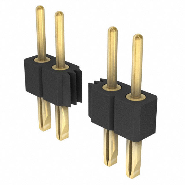
6 Test point for Secondary Control (SC) 7 Output voltage points are designed to accommodate #10 hardware and Panduit ring lugs. 8 Output connector (J01) for mating with VTM-CB providing Vout and VC. As shown on the schematic (Figure 2) there are four pins dedicated to the + Out, four for the -Out, and two for the VC. Each contact is rated for 3 A. The excess capacity afforded by these pins can facilitate testing multiple VTM-CBs from a single PRM-CB using an appropriatewiring harness and mating connector. This may also be achieved using the large pads of Item 7. 9 Output scope jack (J02). Headers H01 and J01 are 0.100" spacing, 10 position female, manufactured by Sullins Electronics and available from Digi-Key as part # S5519-ND. Below is the schematic for this PCB. Double clicking the image will launch Adobe Acrobat to allow you a better view. Figure 2 PRM-CB schematic diagram Recommended Hardware QTY Description Manufacturer P/N 4 ring lug Panduit LCAS6-10-L Kit # 26647 contains: 4 #10-32 screw 4 #10 flat washer 4 #10 lock washer 4 #10 hex nut All hardware is stainless steel except the ring lug. Kit # 26647 is included with the Customer Evaluation Board. UG:003 vicorpower.com Applications Engineering: 800 927.9474 Page 3
Initial Set Up To test the PRM®mounted to the board it is necessary to configure the switch bank (Item 5) as shown on the silk screen in Figure 3. Placing the switch bank in this state connects a fixed resistor between OS and SG of the PRM that sets the output voltage of the PRM to the nominal value indicated on its respective data sheet. Failure to configure the switch bank in this state prior to testing may result in improper output or no output. Baseline Test Procedure - PRM-CB (Refer to Figure 3) 1.0 Recommended Equipment 1.1 DC power supply – 0-100 V; 500 W. 1.2 DC electronic load – pulse capable; 0-100 V; 100 A minimum. 1.3 DMM. 1.4 Oscilloscope. 1.5 Appropriately sized interconnect cables. 1.6 Fastening hardware. 1.7 Fan (if the PRM is to be operated for extended periods of time or at an elevated ambient temperature we recommend the supplied heat sink be installed). 1.8 Safety glasses. 1.9 Data sheet for the requisite PRM. Figure 3 PRM Customer Board Layout switch bank (Item 5) switch reference (silk screen) UG:003 vicorpower.com Applications Engineering: 800 927.9474 Page 4
2.0 Hook Up 2.1 Connect the power supply +Out lead to the +In terminal of the Customer Evaluation Board. 2.2 Connect the power supply –Out lead to the –In terminal of the Customer Evaluation Board. 2.3 A high quality, low-noise power supply should be connected to these locations 2.4 Connect a lead between the +Out of the Customer Evaluation Board and +In of the load. 2.5 Connect a lead between the –Out of the Customer Evaluation Board and –In of the load. 2.6 Connections to these locations should be with short heavy gauge leads. 3.0 Verify Connections 4.0 Test Sequence 4.1 Have the latest version of the PRM®data sheet in hand. 4.2 Assure that the DC supply is set to 0 Vdc prior to turning the unit on. 4.3 Confirm that the switch bank is configured as shown in the silk screen on the board. 4.4 Turn on the DC supply. 4.5 Make sure the DC load is set to constant current and at 0 A prior to turning on the load. 4.6 Turn on the DC load. 4.7 Connect an oscilloscope to the test point provided to monitor output voltage. Many types of scope probes may be directly connected to these points if the probe is equipped with a removable plastic sheath. Be careful to avoid creating ground loops when making measurementsof this voltage and the input voltage. It is recommended that themeasurementsbe made separately. Shorting the -input and -output of the PRM will defeat the PRM current limit feature as the current shunt is in this path. 4.8 Turn on a fan if desired. 4.9 Raise the DC input voltage to the nominal value indicated on the data sheet. 4.10 Verify no load operation by raising and lowering the input voltage through the entire input voltage range. The output voltage should remain constant within the tolerance indicated in the data sheet. 4.11 Re-establish the nominal input voltage. 4.12 Slowly increase the load current to full load while monitoring the output voltage. The output voltage should remain within the limits specified in the appropriate PRM data sheet. 4.13 Return the load current to 0 A and decrease the input voltage to low line. 4.14 Repeat step 4.12. Depending upon the supply used and the source impedance it may be necessary to adjust the input voltage to keep the input to the PRM at low line. 4.15 Return the load current to 0 A and increase the input voltage to high line. 4.16 Repeat step 4.12. 5.0 You have now verified the functionality of the PRM over the entire line and load operating range. 6.0 Deviating from Nominal Settings This board has provisions, as described in the Board Overview section, to adjust the configuration of the PRM about the nominal values. The data sheet for the PRM has equations and curves for determining the required resistor values needed for specific conditions. Applications requiring output voltages other than the nominal setting will need to have the new value set via the trim pots and respective switches. Reference Items 4 and 5 of the Board Overview and the schematic shown in Figure 2. 6.1 Adjust the PRM Output Voltage Set Point 6.1.1 Make sure that the power is removed from the unit prior to making adjustment. 6.1.2 Using a DMM (set to measure resistance), probe between SG (Item 3) and the pad labeled OS located next to the 5 kΩ trim pot R08. UG:003 vicorpower.com Applications Engineering: 800 927.9474 Page 5
6.1.3 Adjust R08 such that the meter reads ~ 200 Ω. This value added to the fixed resistor R07 should total ~ 2.3 kΩ. Note: R07 is 1.7 kΩ on the boards with the MIL-COTS PRM. 6.1.4 One could also probe between SG and the ONside of switch OSV (#5) and set the total resistance shown to ~ 2.3 kΩ. 6.1.5 Move switch OSF (#6) to the OFF position. 6.1.6 Move switch OSV (#5) to the ON position. 6.1.7 The unit is now ready to provide the desired output voltage set point. 6.1.8 Powering the device on should yield a no-load output voltage of the nominal specified value. 6.1.9 The output voltage can now be set to the desired value by varying trim pot OS (R08). 6.1.10 IT MAY BE POSSIBLE TO INADVERTENTLY TRIM THE OUTPUT TOO HIGH ENABLING THE OVERVOLTAGE PROTECTION CIRCUIT. If this happens, reduce the impedance of R08. The initial conditions of steps 6.1.2 and 6.1.3 can be used to recover. 6.1.11 The desired output voltage set point can also be achieved by using the equations in the data sheet and setting the total OS resistance (R07+R08) to that value and then configuring the switches as above. 6.1.12 Be certain to adhere to the power vs. output voltage curve in the data sheet to avoid over powering the device! 6.2 Adjusting the Current Limit 6.2.1 Increasing the load beyond the rated maximum may activate the PRM’s internal current limit (see data sheet for values) feature. Certain applications may require a lower limit and for those situations we offer the adjustment feature. 6.2.2 Refer to the data sheet for the resistance vs. limit curve for the desired limit value. Note: the IL values of resistors installed on this board (R01+R02: 2 kΩ+100 kΩ) may not cover the entire range of the curve. 6.2.3 The adjustable IL mode is engaged by repositioning the IL switch (#2) from OFF to ON. (This may be done while the unit is powered.) 6.2.4 Adjusting the IL trim pot will reduce the current limit from the factory preset limits specified in the data sheet. It is not possible to increase this limit beyond the factory settings. 6.2.5 To reinstate the factory limit return the IL switch to the OFF position. 6.3 Trimming the output voltage using SC 6.3.1 Once the output voltage has been determined and set using the OS resistors, it is still possible to trim the output down to 26 V using the SC control. Adjusting the output in this manner rather than merely adjusting the output via the OS values provides improved regulation. 6.3.2 Depending upon the chosen initial output voltage determined by the OS resistors, the amount of available adjustment might be very limited. Enabling SC adjustment by toggling the SC switch (#3) to the ON position may result in shut down. 6.3.3 To avoid the situation described in 6.3.2, set theSC trim pot R04 (100 kΩ) to its maximum value prior to enabling the switch. 6.3.4 The data sheet has an equation for calculating the appropriate resistor value for a trimmed output voltage. This value would be the sum of fixed resistor R03 (5.11 kΩ) and the trim pot R04. R04 can be set using the test points provided locally, or the sum set using the SC and SG test points (Items 3 and 6) when the SC switch is ON. 6.4 Activating Adaptive Loop Regulation and Interconnect Compensation CD. 6.4.1 The CD switch (#4) and the associated fixed resistor R05 (20 Ω) and trim pot R06 (20 Ω) enable the PRM Adaptive Loop regulation feature, which compensates for the VTM output resistance induced voltage drop as the load current from the VTM is increased. 6.4.2 This feature is intended to be used with mating VTM-CB discussed in detail in the next section. UG:003 vicorpower.com Applications Engineering: 800 927.9474 Page 6
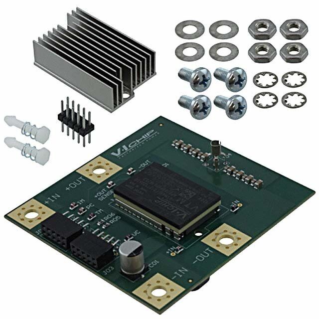
VTM-CB (Figure 4) The VTM®module provides the isolation stage and the output voltage step down. When paired with the PRM the chip set forms a traditional DC-DC converter. The -CB board for the VTM is intended to be used in conjunction with the PRM-CB; nevertheless, in order to test this standalone, it is possible to inject a VC pulse as specified in the data sheet to the exposed lead from the header corresponding to the VC pin. Refer to the board schematic Figure 5 for the appropriate pin(s.) An impedance measurement may prove just as expeditious. 3 Figure 4 VTM-CB 1 5 2 4 3 Board Overview 1 Source voltage input points (Item 1) are designed to accommodate#10 hardware and Panduit ring lugs. BE CERTAIN POLARITY IS CORRECT BEFORE APPLYING POWER. 2 Input connector J01 (Item 2) mates with PRM-CB providing Vin and VC. As can be seen from the following schematic there are four pins dedicated to the + In, four for the -In, and two for the VC. Each contact is rated for 3 A. The excess capacity afforded by these pins can facilitate testing multiple VTM-CBs from a single PRM-CB using an appropriate wiring harness and mating connector. This may also be achieved using the large pads of Item 1. Note:There is a removable male tomale insert installed into this connector. This allows the mate to be either gender which may be important depending upon the availability of connectors. 3 The Kelvin connection points for Vin and Vout (Item 3) are for use in efficiency measurements. 4 The scope jack (Item 4) is used to view output voltage parameters. 5 Output voltage points (Item 5) are designed to accommodate #10 hardware and Panduit ring lugs. UG:003 vicorpower.com Applications Engineering: 800 927.9474 Page 7
Figure 5 Figure 5 is the schematic for this PCB. Double clicking the image will launch Adobe Acrobat to allow VTM-CB schematic diagram you a better view. The DC-DC Converter Chip Set The -CB boards in Figure 6 allow the user to select and configure the PRM®and VTM®to the unique application requirements of their system. By selecting the PRM to accept the desired input voltage, one need only select the VTM to provide the desired output voltage and plug them together if the nominal voltages are all that are required. Figure 6 CB boards UG:003 vicorpower.com Applications Engineering: 800 927.9474 Page 8
For example, if a P048F048T24AL-CB and a V048F120T025-CB are mated as above, the input range to the pair is 36 – 75 Vdc and the output would be 12 Vdc at no load decreasing by Iout x Rout of the VTM®as the load current increases. This Vout decrease is due to the switch bank being configured as shown in the silk screen. In this configuration, the PRM®is set for Local Loop mode as described in Section 5d. To provide for load regulation at the output of the VTM, the Adaptive Loop regulation mode should be engaged. To activate this feature of the PRM-AL, the switch indicated CD (switch #4) should be set to the ON position. The corresponding trim pot should be set to 19.2 Ω which will result in a total CD to SG resistance of 39.2 Ω. This is the optimal value for the nominal PRM output voltage as set by the fixed OS resistor installed on the board and activated by the OSF (switch #6) in the ON position. Be certain to refer to the data sheets for the appropriate resistor values for your requirements. To validate the functionality of the Adaptive Loop regulation, repeat the steps of 2.0 to 5.0 under the section Baseline Test Procedure - PRM-CB except in this instance the output connections are to be made to the VTM-CB output terminals. Both the PRM and VTM data sheets should be in hand.The load current refers to the VTM output current ratings. Be certain to make the connections to the supply and load prior to mating the boards to avoid stressing the connectors. The PRM Adaptive Loop regulates the output of the VTM without sense lines. The Factorized Bus voltage (Vf) may be moniored by using J02 on the PRM-CB board (Item 9) while increasing the load current. Observe the Vf voltage increases with the load current, compensating for the insertion loss due to the VTM output resistance. VTM output voltages, which deviate from the nominal configuration, are available by changing the output set point of the PRM as described in section 6 of this document and using the formula described in the data sheet. Ordering Information The PRM and VTM Customer Evaluation Boards are specified by add the suffix “-CB” to the appropriate PRM or VTM model number. Go to http://www.vicorpower.com/contact-usfor ordering information. 12/2013 vicorpower.com Applications Engineering: 800 927.9474 Rev 1.1 Page 9