ICGOO在线商城 > 集成电路(IC) > PMIC - 配电开关,负载驱动器 > VNN3NV0413TR
 Datasheet下载
- 型号: VNN3NV0413TR
- 制造商: STMicroelectronics
- 库位|库存: xxxx|xxxx
- 要求:
| 数量阶梯 | 香港交货 | 国内含税 |
| +xxxx | $xxxx | ¥xxxx |
查看当月历史价格
查看今年历史价格
VNN3NV0413TR产品简介:
ICGOO电子元器件商城为您提供VNN3NV0413TR由STMicroelectronics设计生产,在icgoo商城现货销售,并且可以通过原厂、代理商等渠道进行代购。 VNN3NV0413TR价格参考。STMicroelectronicsVNN3NV0413TR封装/规格:PMIC - 配电开关,负载驱动器, 。您可以下载VNN3NV0413TR参考资料、Datasheet数据手册功能说明书,资料中有VNN3NV0413TR 详细功能的应用电路图电压和使用方法及教程。
STMicroelectronics(意法半导体)的型号 VNN3NV0413TR 属于 PMIC(电源管理集成电路)中的配电开关和负载驱动器类别。以下是该型号的应用场景分析:

 1. 消费电子设备
   - 便携式设备:如智能手机、平板电脑、可穿戴设备等需要高效电源管理的场景。VNN3NV0413TR 的低导通电阻特性可以减少功耗,延长电池寿命。
   - 音频设备:例如蓝牙耳机、音响系统等,其负载驱动功能能够稳定供电并支持动态负载变化。

 2. 工业自动化
   - 传感器供电:在工业物联网(IIoT)中,传感器网络需要可靠的电源分配,该器件可用于为多个传感器提供独立的电源通道。
   - 电机控制:适用于小型直流电机或步进电机的驱动控制,确保电流供应稳定且安全。

 3. 汽车电子
   - 车载信息娱乐系统:用于管理屏幕、扬声器和其他外设的电源分配。
   - ADAS(高级驾驶辅助系统):为摄像头、雷达模块等关键组件提供精确的电源控制,保障系统运行的可靠性。

 4. 通信设备
   - 基站模块:在5G或4G基站中,用于分配不同子系统的电源,提高整体能效。
   - 路由器与交换机:为内部电路板上的各种模块提供独立的电源管理。

 5. 医疗设备
   - 便携式医疗仪器:如血压计、血糖仪等,要求低功耗和高可靠性的电源管理。
   - 监护设备:如心电图机或脉搏血氧仪,需要稳定的负载驱动能力以确保数据采集准确。

 6. 智能家居
   - 智能灯具:控制LED灯带或其他照明设备的开关及亮度调节。
   - 智能家电:如冰箱、空调等,用于管理压缩机、风扇等部件的电源。

 特性优势
- 低导通电阻(Rds(on)):降低功耗,提高效率。
- 过流保护和热关断:增强系统安全性,防止因过载或短路导致损坏。
- 小型封装:适合空间受限的设计,便于集成到紧凑型产品中。

综上所述,VNN3NV0413TR 广泛应用于需要高效电源管理和负载切换的各类场景,特别适合对能效、可靠性和小型化有较高要求的电子产品。
| 参数 | 数值 |
| 产品目录 | 集成电路 (IC) |
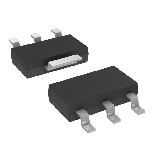
| 描述 | IC MOSFET N-CH 40V 3.5A SOT223 |
| 产品分类 | PMIC - MOSFET,电桥驱动器 - 内部开关 |
| 品牌 | STMicroelectronics |
| 数据手册 | |
| 产品图片 |
|
| 产品型号 | VNN3NV0413TR |
| rohs | 含铅 / 不符合限制有害物质指令(RoHS)规范要求 |
| 产品系列 | OMNIFET II™, VIPower™ |
| 产品培训模块 | http://www.digikey.cn/PTM/IndividualPTM.page?site=cn&lang=zhs&ptm=26261 |
| 产品目录页面 | |
| 供应商器件封装 | SOT-223 |
| 其它名称 | 497-3309-1 |
| 其它有关文件 | http://www.st.com/web/catalog/sense_power/FM1965/CL1969/SC1038/PF65660?referrer=70071840 |
| 包装 | 剪切带 (CT) |
| 安装类型 | 表面贴装 |
| 导通电阻 | 120 毫欧 |
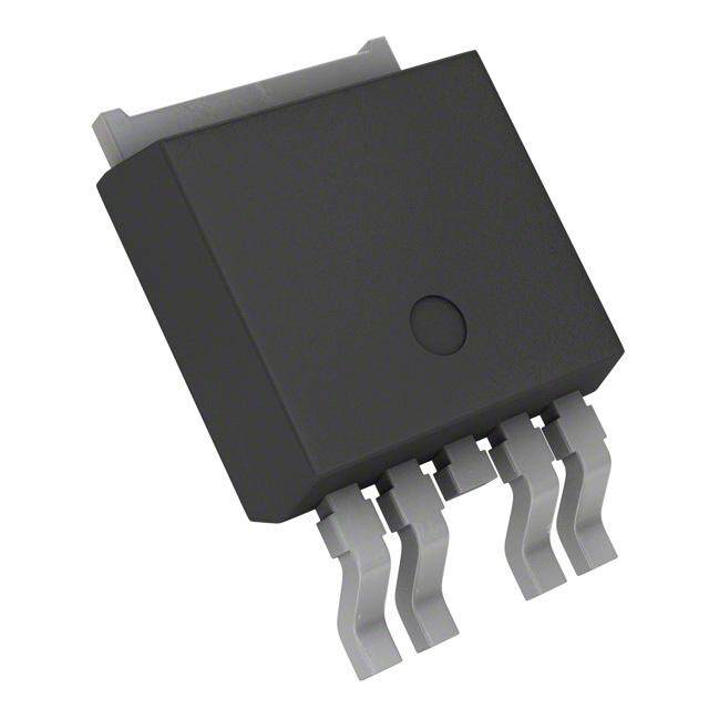
| 封装/外壳 | TO-261-4,TO-261AA |
| 工作温度 | -40°C ~ 150°C |
| 标准包装 | 1 |
| 电压-电源 | - |
| 电流-峰值输出 | 5A |
| 电流-输出/通道 | 3.5A |
| 类型 | 低端 |
| 输入类型 | 非反相 |
| 输出数 | 1 |


- 商务部:美国ITC正式对集成电路等产品启动337调查
- 曝三星4nm工艺存在良率问题 高通将骁龙8 Gen1或转产台积电
- 太阳诱电将投资9.5亿元在常州建新厂生产MLCC 预计2023年完工
- 英特尔发布欧洲新工厂建设计划 深化IDM 2.0 战略
- 台积电先进制程称霸业界 有大客户加持明年业绩稳了
- 达到5530亿美元!SIA预计今年全球半导体销售额将创下新高
- 英特尔拟将自动驾驶子公司Mobileye上市 估值或超500亿美元
- 三星加码芯片和SET,合并消费电子和移动部门,撤换高东真等 CEO
- 三星电子宣布重大人事变动 还合并消费电子和移动部门
- 海关总署:前11个月进口集成电路产品价值2.52万亿元 增长14.8%


PDF Datasheet 数据手册内容提取
VNN3NV04, VNS3NV04 VND3NV04, VND3NV04-1 OMNIFET II fully autoprotected Power MOSFET Features Type RDS(on) Ilim Vclamp 2 VNN3NV04 3 2 VNS3NV04 1 120mΩ 3.5A 40V SOT-223 SO-8 VND3NV04 VND3NV04-1 ■ Linear current limitation ■ Thermal shutdown 3 23 1 1 ■ Short circuit protection TO252 (DPAK) TO251 (IPAK) ■ Integrated clamp ■ Low current drawn from input pin ■ Diagnostic feedback through input pin Description ■ ESD protection ■ Direct access to the gate of the Power The VNN3NV04, VNS3NV04, VND3NV04 MOSFET (analog driving) VND3NV04-1, are monolithic devices designed in STMicroelectronics™ VIPower™ M0-3 ■ Compatible with standard Power MOSFET in Technology, intended for replacement of standard compliance with the 2002/95/EC European Power MOSFETs from DC up to 50kHz Directive applications. Built in thermal shutdown, linear current limitation and overvoltage clamp protect the chip in harsh environments. Fault feedback can be detected by monitoring the voltage at the input pin. Table 1. Device summary Order codes Package Tube Tube (lead-free) Tape and reel Tape and reel (lead-free) SOT-223 VNN3NV04 - VNN3NV0413TR - SO-8 VNS3NV04 - VNS3NV0413TR - TO-252 VND3NV04 VND3NV04-E VND3NV0413TR VND3NV04TR-E TO-251 VND3NV04-1 VND3NV04-1-E - - September 2013 Doc ID 7382 Rev 4 1/26 www.st.com 1
Contents VNN3NV04, VNS3NV04, VND3NV04, VND3NV04-1 Contents 1 Block diagram and pin description . . . . . . . . . . . . . . . . . . . . . . . . . . . . . 5 2 Electrical specifications . . . . . . . . . . . . . . . . . . . . . . . . . . . . . . . . . . . . . . 6 2.1 Absolute maximum ratings . . . . . . . . . . . . . . . . . . . . . . . . . . . . . . . . . . . . . 6 2.2 Thermal data . . . . . . . . . . . . . . . . . . . . . . . . . . . . . . . . . . . . . . . . . . . . . . . 7 2.3 Electrical characteristics . . . . . . . . . . . . . . . . . . . . . . . . . . . . . . . . . . . . . . . 7 3 Protection features . . . . . . . . . . . . . . . . . . . . . . . . . . . . . . . . . . . . . . . . . . 9 3.1 Electrical characteristics curves . . . . . . . . . . . . . . . . . . . . . . . . . . . . . . . . 12 4 Package and packing information . . . . . . . . . . . . . . . . . . . . . . . . . . . . . 16 4.1 ECOPACK® . . . . . . . . . . . . . . . . . . . . . . . . . . . . . . . . . . . . . . . . . . . . . . . 16 4.2 TO-251 (IPAK) mechanical data . . . . . . . . . . . . . . . . . . . . . . . . . . . . . . . . 16 4.3 TO-252 (DPAK) mechanical data . . . . . . . . . . . . . . . . . . . . . . . . . . . . . . . 17 4.4 SOT-223 mechanical data . . . . . . . . . . . . . . . . . . . . . . . . . . . . . . . . . . . . 18 4.5 SO-8 mechanical data . . . . . . . . . . . . . . . . . . . . . . . . . . . . . . . . . . . . . . . 19 4.6 SOT-223 packing information . . . . . . . . . . . . . . . . . . . . . . . . . . . . . . . . . . 21 4.7 SO-8 packing information . . . . . . . . . . . . . . . . . . . . . . . . . . . . . . . . . . . . . 22 4.8 DPAK packing information . . . . . . . . . . . . . . . . . . . . . . . . . . . . . . . . . . . . 23 4.9 IPAK packing information . . . . . . . . . . . . . . . . . . . . . . . . . . . . . . . . . . . . . 24 5 Revision history . . . . . . . . . . . . . . . . . . . . . . . . . . . . . . . . . . . . . . . . . . . 25 2/26 Doc ID 7382 Rev 4
VNN3NV04, VNS3NV04, VND3NV04, VND3NV04-1 List of tables List of tables Table 1. Device summary. . . . . . . . . . . . . . . . . . . . . . . . . . . . . . . . . . . . . . . . . . . . . . . . . . . . . . . . . . 1 Table 2. Absolute maximum ratings. . . . . . . . . . . . . . . . . . . . . . . . . . . . . . . . . . . . . . . . . . . . . . . . . . 6 Table 3. Thermal data. . . . . . . . . . . . . . . . . . . . . . . . . . . . . . . . . . . . . . . . . . . . . . . . . . . . . . . . . . . . . 7 Table 4. Electrical characteristics. . . . . . . . . . . . . . . . . . . . . . . . . . . . . . . . . . . . . . . . . . . . . . . . . . . . 7 Table 5. TO-251 (IPAK) mechanical data. . . . . . . . . . . . . . . . . . . . . . . . . . . . . . . . . . . . . . . . . . . . . 16 Table 6. TO-252 (DPAK) mechanical data. . . . . . . . . . . . . . . . . . . . . . . . . . . . . . . . . . . . . . . . . . . . 17 Table 7. SOT-223 mechanical data . . . . . . . . . . . . . . . . . . . . . . . . . . . . . . . . . . . . . . . . . . . . . . . . . 18 Table 8. SO-8 mechanical data . . . . . . . . . . . . . . . . . . . . . . . . . . . . . . . . . . . . . . . . . . . . . . . . . . . . 19 Table 9. Document revision history . . . . . . . . . . . . . . . . . . . . . . . . . . . . . . . . . . . . . . . . . . . . . . . . . 25 Doc ID 7382 Rev 4 3/26
List of figures VNN3NV04, VNS3NV04, VND3NV04, VND3NV04-1 List of figures Figure 1. Block diagram. . . . . . . . . . . . . . . . . . . . . . . . . . . . . . . . . . . . . . . . . . . . . . . . . . . . . . . . . . . . 5 Figure 2. Configuration diagram (top view) . . . . . . . . . . . . . . . . . . . . . . . . . . . . . . . . . . . . . . . . . . . . . 5 Figure 3. Current and voltage conventions . . . . . . . . . . . . . . . . . . . . . . . . . . . . . . . . . . . . . . . . . . . . . 6 Figure 4. Switching time test circuit for resistive load . . . . . . . . . . . . . . . . . . . . . . . . . . . . . . . . . . . . 10 Figure 5. Test circuit for diode recovery times. . . . . . . . . . . . . . . . . . . . . . . . . . . . . . . . . . . . . . . . . . 10 Figure 6. Unclamped inductive load test circuits . . . . . . . . . . . . . . . . . . . . . . . . . . . . . . . . . . . . . . . . 11 Figure 7. Input charge test circuit. . . . . . . . . . . . . . . . . . . . . . . . . . . . . . . . . . . . . . . . . . . . . . . . . . . . 11 Figure 8. Unclamped inductive waveforms . . . . . . . . . . . . . . . . . . . . . . . . . . . . . . . . . . . . . . . . . . . . 11 Figure 9. Thermal impedance for DPAK/IPAK. . . . . . . . . . . . . . . . . . . . . . . . . . . . . . . . . . . . . . . . . . 12 Figure 10. Thermal impedance for SOT-223. . . . . . . . . . . . . . . . . . . . . . . . . . . . . . . . . . . . . . . . . . . . 12 Figure 11. Derating curve . . . . . . . . . . . . . . . . . . . . . . . . . . . . . . . . . . . . . . . . . . . . . . . . . . . . . . . . . . 12 Figure 12. Transconductance . . . . . . . . . . . . . . . . . . . . . . . . . . . . . . . . . . . . . . . . . . . . . . . . . . . . . . . 12 Figure 13. Static drain-source on resistance vs input voltage (part 1/2) . . . . . . . . . . . . . . . . . . . . . . . 12 Figure 14. Static drain-source on resistance vs input voltage (part 2/2) . . . . . . . . . . . . . . . . . . . . . . . 12 Figure 15. Source-drain diode forward characteristics . . . . . . . . . . . . . . . . . . . . . . . . . . . . . . . . . . . . 13 Figure 16. Static drain source on resistance . . . . . . . . . . . . . . . . . . . . . . . . . . . . . . . . . . . . . . . . . . . . 13 Figure 17. Turn-on current slope (part 1/2) . . . . . . . . . . . . . . . . . . . . . . . . . . . . . . . . . . . . . . . . . . . . . 13 Figure 18. Turn-on current slope (part 2/2) . . . . . . . . . . . . . . . . . . . . . . . . . . . . . . . . . . . . . . . . . . . . . 13 Figure 19. Transfer characteristics . . . . . . . . . . . . . . . . . . . . . . . . . . . . . . . . . . . . . . . . . . . . . . . . . . . 13 Figure 20. Static drain-source on resistance vs Id. . . . . . . . . . . . . . . . . . . . . . . . . . . . . . . . . . . . . . . . 13 Figure 21. Input voltage vs input charge . . . . . . . . . . . . . . . . . . . . . . . . . . . . . . . . . . . . . . . . . . . . . . . 14 Figure 22. Turn-off drain source voltage slope (part 1/2). . . . . . . . . . . . . . . . . . . . . . . . . . . . . . . . . . . 14 Figure 23. Turn-off drain source voltage slope (part 2/2). . . . . . . . . . . . . . . . . . . . . . . . . . . . . . . . . . . 14 Figure 24. Capacitance variations. . . . . . . . . . . . . . . . . . . . . . . . . . . . . . . . . . . . . . . . . . . . . . . . . . . . 14 Figure 25. Output characteristics. . . . . . . . . . . . . . . . . . . . . . . . . . . . . . . . . . . . . . . . . . . . . . . . . . . . . 14 Figure 26. Normalized on resistance vs temperature . . . . . . . . . . . . . . . . . . . . . . . . . . . . . . . . . . . . . 14 Figure 27. Switching time resistive load (part 1/2). . . . . . . . . . . . . . . . . . . . . . . . . . . . . . . . . . . . . . . . 15 Figure 28. Switching time resistive load (part 2/2). . . . . . . . . . . . . . . . . . . . . . . . . . . . . . . . . . . . . . . . 15 Figure 29. Normalized input threshold voltage vs temperature. . . . . . . . . . . . . . . . . . . . . . . . . . . . . . 15 Figure 30. Normalized current limit vs junction temperature . . . . . . . . . . . . . . . . . . . . . . . . . . . . . . . . 15 Figure 31. Step response current limit. . . . . . . . . . . . . . . . . . . . . . . . . . . . . . . . . . . . . . . . . . . . . . . . . 15 Figure 32. TO-251 (IPAK) package dimensions . . . . . . . . . . . . . . . . . . . . . . . . . . . . . . . . . . . . . . . . . 17 Figure 33. TO-252 (DPAK) package dimensions. . . . . . . . . . . . . . . . . . . . . . . . . . . . . . . . . . . . . . . . . 18 Figure 34. SOT-223 package dimensions. . . . . . . . . . . . . . . . . . . . . . . . . . . . . . . . . . . . . . . . . . . . . . 19 Figure 35. SO-8 package dimensions . . . . . . . . . . . . . . . . . . . . . . . . . . . . . . . . . . . . . . . . . . . . . . . . . 20 Figure 36. SOT-223 tape and reel shipment (suffix “TR”) . . . . . . . . . . . . . . . . . . . . . . . . . . . . . . . . . . 21 Figure 37. SO-8 tube shipment (no suffix). . . . . . . . . . . . . . . . . . . . . . . . . . . . . . . . . . . . . . . . . . . . . . 22 Figure 38. SO-8 tape and reel shipment (suffix “TR”) . . . . . . . . . . . . . . . . . . . . . . . . . . . . . . . . . . . . . 22 Figure 39. DPAK footprint and tube shipment (no suffix). . . . . . . . . . . . . . . . . . . . . . . . . . . . . . . . . . . 23 Figure 40. DPAK tape and reel shipment (suffix “TR”) . . . . . . . . . . . . . . . . . . . . . . . . . . . . . . . . . . . . 23 Figure 41. IPAK tube shipment (no suffix). . . . . . . . . . . . . . . . . . . . . . . . . . . . . . . . . . . . . . . . . . . . . . 24 4/26 Doc ID 7382 Rev 4
VNN3NV04, VNS3NV04, VND3NV04, VND3NV04-1 Block diagram and pin description 1 Block diagram and pin description Figure 1. Block diagram DRAIN 2 Overvoltage Clamp INPUT Gate 1 Control Linear Current Over Limiter Temperature 3 SOURCE FC01000 Figure 2. Configuration diagram (top view) SO-8 Package(1) SOURCE 1 8 DRAIN SOURCE DRAIN SOURCE DRAIN INPUT 4 5 DRAIN 1. For the pins configuration related to SOT-223, DPAK, IPAK see outlines at page 1. Doc ID 7382 Rev 4 5/26
Electrical specifications VNN3NV04, VNS3NV04, VND3NV04, VND3NV04-1 2 Electrical specifications Figure 3. Current and voltage conventions I D V DS DRAIN IIN RIN INPUT SOURCE V IN 2.1 Absolute maximum ratings T able 2. Absolute maximum ratings Value Symbol Parameter Unit SOT-223 SO-8 DPAK/IPAK V Drain-source voltage (V =0V) Internally clamped V DS IN V Input voltage Internally clamped V IN I Input current +/-20 mA IN R Minimum input series impedance 220 Ω IN MIN I Drain current Internally limited A D I Reverse DC output current -5.5 A R Electrostatic discharge (R=1.5KΩ, V 4000 V ESD1 C=100pF) Electrostatic discharge on output pin V 16500 V ESD2 only (R=330Ω, C=150pF) P Total dissipation at T=25°C 7 8.3 35 W tot c T Operating junction temperature Internally limited °C j T Case operating temperature Internally limited °C c T Storage temperature -55 to 150 °C stg 6/26 Doc ID 7382 Rev 4
VNN3NV04, VNS3NV04, VND3NV04, VND3NV04-1 Electrical specifications 2.2 Thermal data Table 3. T hermal data Value Symbol Parameter Unit SOT-223 SO-8 DPAK IPAK R Thermal resistance junction-case max 18 3.5 3.5 °C/W thj-case R Thermal resistance junction-lead max 15 °C/W thj-lead R Thermal resistance junction-ambient max 70(1) 65(1) 54(1) 100 °C/W thj-amb 1. When mounted on a standard single-sided FR4 board with 50mm2 of Cu (at least 35mm thick) connected to all DRAIN pins. 2.3 Electrical characteristics -40°C < T < 150°C, unless otherwise specified. j Table 4. E lectrical characteristics Symbol Parameter Test conditions Min Typ Max Unit Off Drain-source clamp V V =0V; I =1.5A 40 45 55 V CLAMP voltage IN D Drain-source clamp V V =0V; I =2mA 36 V CLTH threshold voltage IN D V Input threshold voltage V =V ; I =1mA 0.5 2.5 V INTH DS IN D Supply current from input I V =0V; V =5V 100 150 µA ISS pin DS IN V Input-source clamp IIN=1mA 6 6.8 8 V INCL voltage I =-1mA -1.0 -0.3 IN I Zero input voltage drain VDS=13V; VIN=0V; Tj=25°C 30 µA DSS current (VIN=0V) VDS=25V; VIN=0V 75 On R Static drain-source on VIN=5V; ID=1.5A; Tj=25°C 120 mΩ DS(on) resistance V =5V; I =1.5A 240 IN D Dynamic (T=25°C, unless otherwise specified) j Forward g (1) V =13V; I =1.5A 5.0 S fs transconductance DD D C Output capacitance V =13V; f=1MHz; V =0V 150 pF OSS DS IN Switching (Tj=25°C, unless otherwise specified) Doc ID 7382 Rev 4 7/26
Electrical specifications VNN3NV04, VNS3NV04, VND3NV04, VND3NV04-1 Table 4. Electrical characteristics (continued) Symbol Parameter Test conditions Min Typ Max Unit t Turn-on delay time 90 300 ns d(on) V =15V; I =1.5A t Rise time DD D 250 750 ns r V =5V; R =R =220Ω gen gen IN MIN t Turn-off delay time 450 1350 ns d(off) (see figure Figure 4.) t Fall time 250 750 ns f t Turn-on delay time 0.45 1.35 µs d(on) V =15V; I =1.5A t Rise time DD D 2.5 7.5 µs r V =5V; R =2.2KΩ gen gen t Turn-off delay time 3.3 10.0 µs d(off) (see figure Figure 4.) t Fall time 2.0 6.0 µs f V =15V; I =1.5A (dI/dt) Turn-on current slope DD D 4.7 A/µs on V =5V; R =R =220Ω gen gen IN MIN V =12V; I =1.5A; V =5V Q Total input charge DD D IN 8.5 nC i I =2.13mA (see figure Figure 7.) gen Source drain diode (T=25°C, unless otherwise specified) j V (1) Forward on voltage I =1.5A; V =0V 0.8 V SD SD IN t Reverse recovery time 107 ns rr I =1.5A; dI/dt=12A/µs SD Q Reverse recovery charge V =30V; L=200µH 37 µC rr DD (see test circuit, figure Figure 5.) I Reverse recovery current 0.7 A RRM Protections (-40°C < T < 150°C, unless otherwise specified) j I Drain current limit V =5V; V =13V 3.5 5 7 A lim IN DS Step response current t V =5V; V =13V 10 µs dlim limit IN DS Over temperature T 150 175 200 °C jsh shutdown T Over temperature reset 135 °C jrs I Fault sink current V =5V; V =13V; T=T 10 15 20 mA gf IN DS j jsh starting T=25µ°C; V =24V j DD Single pulse avalanche E V =5V R =R =220Ω; L=24mH 100 mJ as energy IN gen IN MIN (see figures Figure 6. & Figure 8.) 1. Pulsed: Pulse duration = 300µs, duty cycle 1.5% 8/26 Doc ID 7382 Rev 4
VNN3NV04, VNS3NV04, VND3NV04, VND3NV04-1 Protection features 3 Protection features During normal operation, the input pin is electrically connected to the gate of the internal Power MOSFET through a low impedance path. The device then behaves like a standard Power MOSFET and can be used as a switch from DC up to 50kHz. The only difference from the user’s standpoint is that a small DC current I (typ. 100µA) flows into the input pin in order to supply the internal circuitry. ISS The device integrates: ● Overvoltage clamp protection: internally set at 45V, along with the rugged avalanche characteristics of the Power MOSFET stage give this device unrivalled ruggedness and energy handling capability. This feature is mainly important when driving inductive loads. ● Linear current limiter circuit: limits the drain current I to I whatever the input pin D lim voltages. When the current limiter is active, the device operates in the linear region, so power dissipation may exceed the capability of the heatsink. Both case and junction temperatures increase, and if this phase lasts long enough, junction temperature may reach the over temperature threshold T . jsh ● Over temperature and short circuit protection: these are based on sensing the chip temperature and are not dependent on the input voltage. The location of the sensing element on the chip in the power stage area ensures fast, accurate detection of the junction temperature. Over temperature cutout occurs in the range 150 to 190°C, a typical value being 170°C. The device is automatically restarted when the chip temperature falls of about 15°C below shutdown temperature. ● Status feedback: in the case of an over temperature fault condition (T > T ), the j jsh device tries to sink a diagnostic current I through the input pin in order to indicate fault gf condition. If driven from a low impedance source, this current may be used in order to warn the control circuit of a device shutdown. If the drive impedance is high enough so that the input pin driver is not able to supply the current I , the input pin will fall to 0V. gf This will not however affect the device operation: no requirement is put on the current capability of the input pin driver except to be able to supply the normal operation drive current I . ISS Additional features of this device are ESD protection according to the Human Body model and the ability to be driven from a TTL logic circuit. Doc ID 7382 Rev 4 9/26
Protection features VNN3NV04, VNS3NV04, VND3NV04, VND3NV04-1 Figure 4. Switching time test circuit for resistive load VD I Rgen D Vgen 90% tr 10% tf t V td(on) td(off) gen t Figure 5. Test circuit for diode recovery times A A D I OMNIFET FDAIOSDTE L=100uH S B B 220Ω D Rgen VDD I OMNIFET Vgen S 8.5 Ω 10/26 Doc ID 7382 Rev 4
VNN3NV04, VNS3NV04, VND3NV04, VND3NV04-1 Protection features Figure 6. Unclamped inductive load test Figure 7. Input charge test circuit circuits Figure 8. Unclamped inductive waveforms VIN GEN ND8003 Doc ID 7382 Rev 4 11/26
Protection features VNN3NV04, VNS3NV04, VND3NV04, VND3NV04-1 3.1 Electrical characteristics curves Figure 9. Thermal impedance for DPAK/IPAK Figure 10. Thermal impedance for SOT-223 Figure 11. Derating curve Figure 12. Transconductance Gfs (S) 11 10 9 Vds=13V Tj=-40ºC Tj=25ºC 8 Tj=150ºC 7 6 5 4 3 2 1 0 0 0.5 1 1.5 2 2.5 3 3.5 4 4.5 5 5.5 Id (A) Figure 13. Static drain-source on resistance Figure 14. Static drain-source on resistance vs input voltage (part 1/2) vs input voltage (part 2/2) Rds(on) (mohms) Rds(on) (mohms) 300 250 275 225 250 Id=1.5A 200 225 Tj=150ºC 175 200 Tj=150ºC 175 Id=3.5A 150 Id=1A 150 125 125 Tj=25ºC 100 100 75 Tj=-40ºC IIdd==31.A5A 75 Tj=25ºC 50 IIdd==31.A5A 50 Tj=-40ºC 25 25 0 0 3 3.5 4 4.5 5 5.5 6 6.5 3 3.5 4 4.5 5 5.5 6 6.5 Vin(V) Vin(V) 12/26 Doc ID 7382 Rev 4
VNN3NV04, VNS3NV04, VND3NV04, VND3NV04-1 Protection features Figure 15. Source-drain diode forward Figure 16. Static drain source on resistance characteristics Vsd (mV) Rds(on) (ohms) 1100 4.5 1050 4 Tj=-40ºC Vin=0V 1000 Vin=2.5V 3.5 950 3 900 2.5 850 2 800 750 1.5 Tj=25ºC 700 1 Tj=150ºC 650 0.5 600 0 0 1 2 3 4 5 6 7 8 9 10 11 12 0 0.05 0.1 0.15 0.2 0.25 0.3 Id (A) Id(A) Figure 17. Turn-on current slope (part 1/2) Figure 18. Turn-on current slope (part 2/2) di/dt(A/usec) di/dt(A/us) 1.75 5 4.5 1.5 Vin=5V 4 Vdd=15V Vin=3.5V Id=1.5A 1.25 Vdd=15V 3.5 Id=1.5A 3 1 2.5 0.75 2 1.5 0.5 1 0.5 0.25 0 0 0 250 500 750 1000 1250 1500 1750 2000 2250 2500 0 250 500 750 1000 1250 1500 1750 2000 2250 2500 Rg(ohm) Rg(ohm) Figure 19. Transfer characteristics Figure 20. Static drain-source on resistance vs Id Rds(on) (mohms) Idon(A) 250 2.25 Tj=25ºC 225 2 Vin=5V Vds=13.5V 200 1.75 Tj=150ºC 175 1.5 150 1.25 125 1 Tj=150ºC Tj=25ºC Tj=-40ºC 100 0.75 75 0.5 50 0.25 Tj= - 40ºC 25 0 1.5 2 2.5 3 3.5 4 4.5 5 0 1.75 2.25 2.75 3.25 3.75 4.25 4.75 0 0.5 1 1.5 2 2.5 3 3.5 4 Vin(V) Id (A) Doc ID 7382 Rev 4 13/26
Protection features VNN3NV04, VNS3NV04, VND3NV04, VND3NV04-1 Figure 21. Input voltage vs input charge Figure 22. Turn-off drain source voltage slope (part 1/2) Vin (V) dv/dt(V/usec) 6 300 275 5 250 Vin=5V VIdd=s0=.152AV 225 VIdd=d1=.155AV 4 200 175 3 150 125 100 2 75 50 1 25 0 0 0 500 1000 1500 2000 2500 0 1 2 3 4 5 6 250 750 1250 1750 2250 Qg (nC) Rg(ohm) Figure 23. Turn-off drain source voltage slope Figure 24. Capacitance variations (part 2/2) dv/dt(V/usec) C(pF) 300 350 275 250 Vin=3.5V 300 Vdd=15V 225 Id=1.5A fV=i1nM=0HVz 200 250 175 150 200 125 100 150 75 50 100 25 0 50 0 500 1000 1500 2000 2500 0 5 10 15 20 25 30 35 250 750 1250 1750 2250 Vds(V) Rg(ohm) Figure 25. Output characteristics Figure 26. Normalized on resistance vs temperature v Id (A) Rds(on) (mOhm) 5 4 4.5 Vin=5V 4 Vin=4V 3.5 Vin=5V Id=1.5A 3.5 3 Vin=3V 3 2.5 2.5 2 2 1.5 1.5 1 1 0.5 0 0.5 0 1 2 3 4 5 6 7 8 9 10 -50 -25 0 25 50 75 100 125 150 175 Vds (V) Tc )ºC) 14/26 Doc ID 7382 Rev 4
VNN3NV04, VNS3NV04, VND3NV04, VND3NV04-1 Protection features Figure 27. Switching time resistive load (part Figure 28. Switching time resistive load (part 1/2) 2/2) t(usec) t(nsec) 4 900 3.5 800 Vdd=15V td(off) tr Vdd=15V 3 Id=1.5A 700 Id=1.5A Vin=5V tr Rg=220ohm 2.5 600 2 500 tf 1.5 400 td(off) 1 300 tf 0.5 td(on) 200 td(on) 100 0 0 500 1000 1500 2000 2500 0 250 750 1250 1750 2250 3.25 3.5 3.75 4 4.25 4.5 4.75 5 5.25 Rg(ohm) Vin(V) Figure 29. Normalized input threshold voltage Figure 30. Normalized current limit vs junction vs temperature temperature Ilim (A) Vinth (V) 10 2 9 1.8 Vin=5V 1.6 Vds=Vin 8 Vds=13V Id=1mA 7 1.4 1.2 6 1 5 0.8 4 0.6 3 0.4 2 0.2 1 0 -50 -25 0 25 50 75 100 125 150 175 0 Tc (ºC) -50 -25 0 25 50 75 100 125 150 175 Tc (ºC) Figure 31. Step response current limit Tdlim(usec) 13 12.5 Vin=5V 12 Rg=220ohm 11.5 11 10.5 10 9.5 9 8.5 8 7.5 5 7.5 10 12.5 15 17.5 20 22.5 25 27.5 30 32.5 Vdd(V) Doc ID 7382 Rev 4 15/26
Package and packing information VNN3NV04, VNS3NV04, VND3NV04, VND3NV04-1 4 Package and packing information ® 4.1 ECOPACK In order to meet environmental requirements, ST offers these devices in different grades of ECOPACK® packages, depending on their level of environmental compliance. ECOPACK® specifications, grade definitions and product status are available at: www.st.com. ECOPACK® is an ST trademark. 4.2 TO-251 (IPAK) mechanical data T able 5. TO-251 (IPAK) mechanical data millimeters Symbol Min. Typ. Max. A 2.2 2.4 A1 0.9 1.1 A3 0.7 1.3 B 0.64 0.9 B2 5.2 5.4 B3 0.85 B5 0.3 B6 0.95 C 0.45 0.6 C2 0.48 0.6 D 6 6.2 E 6.4 6.6 G 4.4 4.6 H 15.9 16.3 L 9 9.4 L1 0.8 1.2 L2 0.8 1 16/26 Doc ID 7382 Rev 4
VNN3NV04, VNS3NV04, VND3NV04, VND3NV04-1 Package and packing information Figure 32. TO-251 (IPAK) package dimensions 4.3 TO-252 (DPAK) mechanical data T able 6. TO-252 (DPAK) mechanical data millimeters Symbol Min. Typ. Max. A 2.20 2.40 A1 0.90 1.10 A2 0.03 0.23 B 0.64 0.90 B2 5.20 5.40 C 0.45 0.60 C2 0.48 0.60 D 6.00 6.20 D1 5.1 E 6.40 6.60 E1 4.7 e 2.28 G 4.40 4.60 H 9.35 10.10 Doc ID 7382 Rev 4 17/26
Package and packing information VNN3NV04, VNS3NV04, VND3NV04, VND3NV04-1 Table 6. TO-252 (DPAK) mechanical data (continued) millimeters Symbol Min. Typ. Max. L2 0.8 L4 0.60 1.00 R 0.2 V2 0° 8° Package Weight Gr. 0.29 Figure 33. TO-252 (DPAK) package dimensions P032P 4.4 SOT-223 mechanical data T able 7. SOT-223 mechanical data millimeters Symbol Min. Typ. Max. A 1.8 B 0.6 0.7 0.85 B1 2.9 3 3.15 c 0.24 0.26 0.35 D 6.3 6.5 6.7 e 2.3 18/26 Doc ID 7382 Rev 4
VNN3NV04, VNS3NV04, VND3NV04, VND3NV04-1 Package and packing information Table 7. SOT-223 mechanical data (continued) millimeters Symbol Min. Typ. Max. e1 4.6 E 3.3 3.5 3.7 H 6.7 7 7.3 V 10 (max) A1 0.02 0.1 Figure 34. SOT-223 package dimensions 0046067 4.5 SO-8 mechanical data T able 8. SO-8 mechanical data millimeters Symbol Min Typ Max A 1.75 a1 0.1 0.25 a2 1.65 a3 0.65 0.85 b 0.35 0.48 A 1.75 A1 0.10 0.25 Doc ID 7382 Rev 4 19/26
Package and packing information VNN3NV04, VNS3NV04, VND3NV04, VND3NV04-1 Table 8. SO-8 mechanical data (continued) millimeters Symbol Min Typ Max A2 1.25 b 0.28 0.48 c 0.17 0.23 D(1) 4.80 4.90 5.00 E 5.80 6.00 6.20 E1(2) 3.80 3.90 4.00 e 1.27 h 0.25 0.50 L 0.40 1.27 L1 1.04 k 0° 8° ccc 0.10 1. Dimension “D” does not include mold flash, protrusions or gate burrs. Mold flash, protrusions or gate burrs shall not exceed 0.15mm in total (both side). 2. Dimension “E1” does not include interlead flash or protrusions. Interlead flash or protrusions shall not exceed 0.25mm per side. Figure 35. SO-8 package dimensions 0016023 D 20/26 Doc ID 7382 Rev 4
VNN3NV04, VNS3NV04, VND3NV04, VND3NV04-1 Package and packing information 4.6 SOT-223 packing information Figure 36. SOT-223 tape and reel shipment (suffix “TR”) REEL DIMENSIONS Base Q.ty 1000 Bulk Q.ty 1000 A (max) 330 B (min) 1.5 C (± 0.2) 13 F 20.2 G (+ 2 / -0) 12.4 N (min) 60 T (max) 18.4 TAPE DIMENSIONS According to Electronic Industries Association (EIA) Standard 481 rev. A, Feb. 1986 Tape width W 12 Tape Hole Spacing P0 (± 0.1) 4 Component Spacing P 8 Hole Diameter D (± 0.1/-0) 1.5 Hole Diameter D1 (min) 1.5 Hole Position F (± 0.05) 5.5 Compartment Depth K (max) 4.5 Hole Spacing P1 (± 0.1) 2 All dimensions are in mm. End Start Top No components Components No components cover tape 500mm min Empty components pockets 500mm min saled with cover tape. User direction of feed Doc ID 7382 Rev 4 21/26
Package and packing information VNN3NV04, VNS3NV04, VND3NV04, VND3NV04-1 4.7 SO-8 packing information Figure 37. SO-8 tube shipment (no suffix) B C Base Q.ty 100 Bulk Q.ty 2000 Tube length (± 0.5) 532 A A 3.2 B 6 C (± 0.1) 0.6 Figure 38. SO-8 tape and reel shipment (suffix “TR”) REEL DIMENSIONS Base Q.ty 2500 Bulk Q.ty 2500 A (max) 330 B (min) 1.5 C (± 0.2) 13 F 20.2 G (+ 2 / -0) 12.4 N (min) 60 T (max) 18.4 All dimensions are in mm. TAPE DIMENSIONS According to Electronic Industries Association (EIA) Standard 481 rev. A, Feb 1986 Tape width W 12 Tape Hole Spacing P0 (± 0.1) 4 Component Spacing P 8 Hole Diameter D (± 0.1/-0) 1.5 Hole Diameter D1 (min) 1.5 Hole Position F (± 0.05) 5.5 Compartment Depth K (max) 4.5 Hole Spacing P1 (± 0.1) 2 All dimensions are in mm. End Start Top No components Components No components cover tape 500mm min Empty components pockets 500mm min saled with cover tape. User direction of feed 22/26 Doc ID 7382 Rev 4
VNN3NV04, VNS3NV04, VND3NV04, VND3NV04-1 Package and packing information 4.8 DPAK packing information Figure 39. DPAK footprint and tube shipment (no suffix) A 6.7 1.8 3.0 1.6 C Base Q.ty 75 Bulk Q.ty 3000 2.3 Tube length (± 0.5) 532 6.7 2.3 A 6 B B 21.3 C (± 0.1) 0.6 Figure 40. DPAK tape and reel shipment (suffix “TR”) REEL DIMENSIONS Base Q.ty 2500 Bulk Q.ty 2500 A (max) 330 B (min) 1.5 C (± 0.2) 13 F 20.2 G (+ 2 / -0) 16.4 N (min) 60 T (max) 22.4 TAPE DIMENSIONS According to Electronic Industries Association (EIA) Standard 481 rev. A, Feb 1986 Tape width W 16 Tape Hole Spacing P0 (± 0.1) 4 Component Spacing P 8 Hole Diameter D (± 0.1/-0) 1.5 Hole Diameter D1 (min) 1.5 Hole Position F (± 0.05) 7.5 Compartment Depth K (max) 6.5 Hole Spacing P1 (± 0.1) 2 All dimensions are in mm. End Start Top No components Components No components cover tape 500mm min Empty components pockets 500mm min saled with cover tape. User direction of feed Doc ID 7382 Rev 4 23/26
Package and packing information VNN3NV04, VNS3NV04, VND3NV04, VND3NV04-1 4.9 IPAK packing information Figure 41. IPAK tube shipment (no suffix) A C Base Q.ty 75 Bulk Q.ty 3000 Tube length (± 0.5) 532 B A 6 B 21.3 C (± 0.1) 0.6 All dimensions are in mm. 24/26 Doc ID 7382 Rev 4
VNN3NV04, VNS3NV04, VND3NV04, VND3NV04-1 Revision history 5 Revision history T able 9. Document revision history Date Revision Changes 01-Feb-2003 1 Initial Release Added Table1: Device summary on page1 27-Apr-2009 2 Updated Table4: Package and packing information on page16 Table2: Absolute maximum ratings: 05-Apr-2011 3 – R : changed unit from W to Ω IN MIN Inserted Section4.1: ECOPACK® 20-Sep-2013 4 Updated Disclaimer. Doc ID 7382 Rev 4 25/26
VNN3NV04, VNS3NV04, VND3NV04, VND3NV04-1 Please Read Carefully: Information in this document is provided solely in connection with ST products. STMicroelectronics NV and its subsidiaries (“ST”) reserve the right to make changes, corrections, modifications or improvements, to this document, and the products and services described herein at any time, without notice. All ST products are sold pursuant to ST’s terms and conditions of sale. Purchasers are solely responsible for the choice, selection and use of the ST products and services described herein, and ST assumes no liability whatsoever relating to the choice, selection or use of the ST products and services described herein. No license, express or implied, by estoppel or otherwise, to any intellectual property rights is granted under this document. If any part of this document refers to any third party products or services it shall not be deemed a license grant by ST for the use of such third party products or services, or any intellectual property contained therein or considered as a warranty covering the use in any manner whatsoever of such third party products or services or any intellectual property contained therein. UNLESS OTHERWISE SET FORTH IN ST’S TERMS AND CONDITIONS OF SALE ST DISCLAIMS ANY EXPRESS OR IMPLIED WARRANTY WITH RESPECT TO THE USE AND/OR SALE OF ST PRODUCTS INCLUDING WITHOUT LIMITATION IMPLIED WARRANTIES OF MERCHANTABILITY, FITNESS FOR A PARTICULAR PURPOSE (AND THEIR EQUIVALENTS UNDER THE LAWS OF ANY JURISDICTION), OR INFRINGEMENT OF ANY PATENT, COPYRIGHT OR OTHER INTELLECTUAL PROPERTY RIGHT. ST PRODUCTS ARE NOT DESIGNED OR AUTHORIZED FOR USE IN: (A) SAFETY CRITICAL APPLICATIONS SUCH AS LIFE SUPPORTING, ACTIVE IMPLANTED DEVICES OR SYSTEMS WITH PRODUCT FUNCTIONAL SAFETY REQUIREMENTS; (B) AERONAUTIC APPLICATIONS; (C) AUTOMOTIVE APPLICATIONS OR ENVIRONMENTS, AND/OR (D) AEROSPACE APPLICATIONS OR ENVIRONMENTS. WHERE ST PRODUCTS ARE NOT DESIGNED FOR SUCH USE, THE PURCHASER SHALL USE PRODUCTS AT PURCHASER’S SOLE RISK, EVEN IF ST HAS BEEN INFORMED IN WRITING OF SUCH USAGE, UNLESS A PRODUCT IS EXPRESSLY DESIGNATED BY ST AS BEING INTENDED FOR “AUTOMOTIVE, AUTOMOTIVE SAFETY OR MEDICAL” INDUSTRY DOMAINS ACCORDING TO ST PRODUCT DESIGN SPECIFICATIONS. PRODUCTS FORMALLY ESCC, QML OR JAN QUALIFIED ARE DEEMED SUITABLE FOR USE IN AEROSPACE BY THE CORRESPONDING GOVERNMENTAL AGENCY. Resale of ST products with provisions different from the statements and/or technical features set forth in this document shall immediately void any warranty granted by ST for the ST product or service described herein and shall not create or extend in any manner whatsoever, any liability of ST. ST and the ST logo are trademarks or registered trademarks of ST in various countries. Information in this document supersedes and replaces all information previously supplied. The ST logo is a registered trademark of STMicroelectronics. All other names are the property of their respective owners. © 2013 STMicroelectronics - All rights reserved STMicroelectronics group of companies AusMtraallaiay s- iBa e- lgMiuamlta - - B Mraozroil c-c Coa -n Pahdiali p-p Cinheinsa - -S Cinzgeacpho Rree -p Subplaicin - -F Sinwlaendde n- F- rSawncitez e- rGlaenrdm -a Unny it-e Hdo Knign gKdoonmg -- UInndiitae d- ISstraateels - oItfa Alym - eJraicpaan - www.st.com 26/26 Doc ID 7382 Rev 4