ICGOO在线商城 > 集成电路(IC) > PMIC - 配电开关,负载驱动器 > VND7030AJTR-E

 Datasheet下载
- 型号: VND7030AJTR-E
- 制造商: STMicroelectronics
- 库位|库存: xxxx|xxxx
- 要求:
| 数量阶梯 | 香港交货 | 国内含税 |
| +xxxx | $xxxx | ¥xxxx |
查看当月历史价格
查看今年历史价格
VND7030AJTR-E产品简介:
ICGOO电子元器件商城为您提供VND7030AJTR-E由STMicroelectronics设计生产,在icgoo商城现货销售,并且可以通过原厂、代理商等渠道进行代购。 VND7030AJTR-E价格参考。STMicroelectronicsVND7030AJTR-E封装/规格:PMIC - 配电开关,负载驱动器, 。您可以下载VND7030AJTR-E参考资料、Datasheet数据手册功能说明书,资料中有VND7030AJTR-E 详细功能的应用电路图电压和使用方法及教程。
STMicroelectronics的VND7030AJTR-E是一款PMIC(电源管理集成电路)中的配电开关和负载驱动器,适用于多种应用场景。以下是其主要应用领域:

 1. 汽车电子
VND7030AJTR-E广泛应用于汽车电子系统中,尤其是车身控制模块(BCM)、座椅调节、车窗升降、雨刷控制等需要高可靠性和耐久性的场合。它能够为这些系统提供稳定的电源管理和负载驱动功能,确保车辆电气系统的正常运行。

 2. 工业自动化
在工业自动化设备中,VND7030AJTR-E可用于电机驱动、传感器供电、阀门控制等场景。它能够承受工业环境中的电压波动和电磁干扰,确保设备的稳定性和安全性。此外,该器件支持过流保护和热关断功能,进一步提高了系统的可靠性。

 3. 消费类电子产品
对于消费类电子产品,如智能家居设备、电动工具、家电等,VND7030AJTR-E可以用于驱动小型电机、风扇、泵等负载。它的低导通电阻和高效能特性有助于延长电池寿命,减少能耗,同时保证设备的性能和稳定性。

 4. 通信设备
在通信基站、路由器、交换机等网络设备中,VND7030AJTR-E可以用于电源分配和负载切换。它能够在高频率和大电流条件下保持良好的性能,确保通信设备的持续稳定运行,并且具备快速响应能力,适应瞬态负载变化。

 5. 医疗设备
在医疗设备中,如便携式诊断仪器、监护仪等,VND7030AJTR-E可以用于驱动传感器、显示屏和其他关键组件。其高精度的电源管理和负载驱动功能,确保了医疗设备的准确性和可靠性,同时符合严格的医疗安全标准。

总之,VND7030AJTR-E凭借其高效、可靠和灵活的特点,适用于多种需要精确电源管理和负载驱动的应用场景,尤其是在对安全性和稳定性要求较高的领域。
| 参数 | 数值 |
| 产品目录 | 集成电路 (IC) |
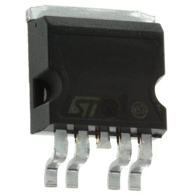
| 描述 | IC DVR HIGH-SIDE 2CH POWERSSO-16 |
| 产品分类 | PMIC - MOSFET,电桥驱动器 - 内部开关 |
| 品牌 | STMicroelectronics |
| 数据手册 | |
| 产品图片 |
|
| 产品型号 | VND7030AJTR-E |
| rohs | 无铅 / 符合限制有害物质指令(RoHS)规范要求 |
| 产品系列 | VIPower™ |
| 供应商器件封装 | PowerSSO-16 |
| 其它名称 | 497-14304-1 |
| 包装 | 剪切带 (CT) |
| 安装类型 | 表面贴装 |
| 导通电阻 | 31 毫欧 |
| 封装/外壳 | 16-PowerLFSOP (0.154", 3.90mm 宽) |
| 工作温度 | -40°C ~ 150°C |
| 标准包装 | 1 |
| 电压-电源 | 4 V ~ 28 V |
| 电流-峰值输出 | - |
| 电流-输出/通道 | 40A |
| 类型 | 高端 |
| 输入类型 | 非反相 |
| 输出数 | 2 |
| 配用 | /product-detail/zh/EV-VND7030AJ/497-14931-ND/4966201 |


- 商务部:美国ITC正式对集成电路等产品启动337调查
- 曝三星4nm工艺存在良率问题 高通将骁龙8 Gen1或转产台积电
- 太阳诱电将投资9.5亿元在常州建新厂生产MLCC 预计2023年完工
- 英特尔发布欧洲新工厂建设计划 深化IDM 2.0 战略
- 台积电先进制程称霸业界 有大客户加持明年业绩稳了
- 达到5530亿美元!SIA预计今年全球半导体销售额将创下新高
- 英特尔拟将自动驾驶子公司Mobileye上市 估值或超500亿美元
- 三星加码芯片和SET,合并消费电子和移动部门,撤换高东真等 CEO
- 三星电子宣布重大人事变动 还合并消费电子和移动部门
- 海关总署:前11个月进口集成电路产品价值2.52万亿元 增长14.8%


PDF Datasheet 数据手册内容提取
EV-VND7030AJ VND7030AJ evaluation board Data brief Diagnostic functions Multiplexed analog feedback of: load current with high precision proportional current mirror, V supply voltage and CC T device temperature CHIP Overload and short to ground (power limitation) indication Thermal shutdown indication OFF-state open-load detection Output short to V detection CC Sense enable/disable Protections Features Undervoltage shutdown Overvoltage clamp Max transient supply voltage V 40 V Load current limitation CC Self limiting of fast thermal transients Operating voltage range V 4 to 28 V CC Configurable latch-off on Typ. on-state resistance (per Ch) RON 31 mΩ overtemperature or power limitation with dedicated fault reset pin Current limitation (typ) I 56 A LIMH Loss of ground and loss of V CC Stand-by current (max) I 0.5 µA STBY Reverse battery with external components Electrostatic discharge protection Simple single IC application board dedicated for VND7030AJ Applications Provides electrical connectivity and thermal heat-sinking for easy prototyping Typical applications are all types of automotive General device features resistive, inductive and capacitive loads. Double channel smart high-side driver Table 1: Device summary with MultiSense analog feedback Very low standby current Order code Reference Compatible with 3 V and 5 V CMOS EV-VND7030AJ VND7030AJ evaluation board outputs September 2015 DocID026359 Rev 3 1/7 www.st.com
Description EV-VND7030AJ 1 Description This board provides you an easy way to connect STMicroelectronics® VIPower® M0-7 technology into your existing system. The board comes pre-assembled with VND7030AJ high-side driver. On board minimum set of electrical components (as for device datasheet recommendation) is enabling the user to directly connect the load, the power supply and the microcontroller without any additional effort in external component design and connection. The VND7030AJ is a double channel high-side driver manufactured using ST proprietary VIPower technology and housed in PowerSSO-16 package. The device is designed to drive 12 V automotive grounded loads through a 3 V and 5 V CMOS-compatible interface and to provide protection and diagnostics. The device integrates advanced protective functions such as load current limitation, overload active management by power limitation and overtemperature shutdown with configurable latch-off. A FaultRST pin unlatches the output in case of fault or disables the latch-off functionality. A dedicated multifunction multiplexed analog output pin delivers sophisticated diagnostic functions including high precision proportional load current sense, supply voltage feedback and chip temperature sense, in addition to the detection of overload and short circuit to ground, short to V and OFF-state open-load. A sense enable pin allows OFF-state CC diagnosis to be disabled during the module low-power mode as well as external sense resistor sharing among similar devices. Figure 1: Evaluation board schematic Vbat Vbat J1 C1 100nF 12345678910 Vbat PGND In_PullUP J2 0 U1 R_UP1 R_UP2 IISSSMFINnNaE_E_u01uELLPltli1N0tuSRlelSUnTsPe +5V J31234567891111110234 Mul1tiC0Sn3eFnPseGNDRR5s e1n5sKePGIINNN01D TTPP1112FSa_uElNtRRSSREE12S LL11T0155KKRRRR4367 11115555KKKK 52364781 SFSSGMIINNaEEENuPPuLnLlDtUUli01tSRTTeS10nTse VBATT OOOOOOOOUUUUUUUUTTTTTTTTPPPPPPPPUUUUUUUUTTTTTTTT00001111 111111191206543 Out0O1ut12 15 PSS0-16 111678 ES1DD1L R4K87 CON18 PGND LED1 LED2 C4 C2 10nF 10nF 12345678910 R9 R10 PGND 2k2 2k2 J4 PGND PGND GAPG1704141132CFT 2/7 DocID026359 Rev 3
EV-VND7030AJ Board connections 2 Board connections Figure 2: "Evaluation board connections" shows the placement of the connectors to be used for supplying the evaluation board, connecting the load and controlling the functionality and diagnostic of the device. Figure 2: Evaluation board connections Table 2: J3 connector: pin functions Pin Connector Pin name Pin function number J3 1…4 N/A Not connected Connection to optional external pull-up resistor for open load J3 5 IN_PullUP detection in off-state. J3 6 +5V 5 V Power Supply Active low compatible with 3 V and 5 V CMOS outputs pin; it J3 7 FaultRST unlatches the output in case of fault; If kept low, sets the outputs in auto-restart Multiplexed analog sense output pin; it delivers a current J3 8 MultiSense proportional to the selected diagnostic: load current, supply voltage or chip temperature Active high compatible with 3 V and 5 V CMOS outputs pin; J3 9 S_EN it enables the MultiSense diagnostic pin. Active high compatible with 3 V and 5 V CMOS outputs pin; J3 10 SEL0 together with SEL1, it addresses the MultiSense multiplexer Active high compatible with 3 V and 5 V CMOS outputs pin; J3 11 SEL1 together with SEL0, it addresses the MultiSense multiplexer J3 12 N/A Not connected Voltage controlled input pin with hysteresis, compatible with J3 13 IN0 3 V and 5 V CMOS outputs. It controls OUT0 switch state Voltage controlled input pin with hysteresis, compatible with J3 14 IN1 3 V and 5 V CMOS outputs. It controls OUT1 switch state J3 15…18 N/A Not connected DocID026359 Rev 3 3/7
Board connections EV-VND7030AJ In case the user wishes to utilize the Current Sense/MultiSense function of the device, it is necessary to plug a sense resistor in R . SENSE The package includes a through-hole resistor, to be mounted on TP1-TP2 (see Figure 4: "Mounting through-hole sense resistor"). Different R values can be adopted based on user preference. SENSE Another option is soldering an SMD resistor on the dedicated PCB pad, as shown in Figure 5: "Pads for soldering SMD resistor". Figure 3: No sense resistor Figure 4: Mounting through-hole sense resistor Figure 5: Pads for soldering SMD resistor 4/7 DocID026359 Rev 3
EV-VND7030AJ Thermal data 3 Thermal data Table 3: Thermal data Symbol Parameter Max Unit R Thermal resistance junction-ambient (MAX) 39 °C/W thj-amb Table 4: PCB specifications Parameter Value Board dimensions 25 mm x 41.5 mm Number of Cu layer 2 Layer Cu thickness 35 μm Board finish thickness 1.6 mm +/- 10% Board Material FR4 Thermal vias separation 1.1 mm Thermal vias diameter 0.5 mm DocID026359 Rev 3 5/7
Revision history EV-VND7030AJ 4 Revision history Table 5: Revision history Revis Date Changes ion 15-May-2014 1 Initial release. 21-Jul-2014 2 Updated Figure 1: "Evaluation board schematic" Changed EV-VND7030AJ-E in EV-VND7030AJ. Updated Section 01-Sep-2015 3 "Features" and Section 1: "Description" 6/7 DocID026359 Rev 3
EV-VND7030AJ IMPORTANT NOTICE – PLEASE READ CAREFULLY STMicroelectronics NV and its subsidiaries (“ST”) reserve the right to make changes, corrections, enhancements, modifications, and improvements to ST products and/or to this document at any time without notice. Purchasers should obtain the latest relevant information on ST products before placing orders. ST products are sold pursuant to ST’s terms and conditions of sale in place at the time of order acknowledgement. Purchasers are solely responsible for the choice, selection, and use of ST products and ST assumes no liability for application assistance or the design of Purchasers’ products. No license, express or implied, to any intellectual property right is granted by ST herein. Resale of ST products with provisions different from the information set forth herein shall void any warranty granted by ST for such product. ST and the ST logo are trademarks of ST. All other product or service names are the property of their respective owners. Information in this document supersedes and replaces information previously supplied in any prior versions of this document. © 2015 STMicroelectronics – All rights reserved DocID026359 Rev 3 7/7