ICGOO在线商城 > 集成电路(IC) > PMIC - AC-DC 转换器,离线开关 > VIPER26LD

 Datasheet下载
- 型号: VIPER26LD
- 制造商: STMicroelectronics
- 库位|库存: xxxx|xxxx
- 要求:
| 数量阶梯 | 香港交货 | 国内含税 |
| +xxxx | $xxxx | ¥xxxx |
查看当月历史价格
查看今年历史价格
VIPER26LD产品简介:
ICGOO电子元器件商城为您提供VIPER26LD由STMicroelectronics设计生产,在icgoo商城现货销售,并且可以通过原厂、代理商等渠道进行代购。 VIPER26LD价格参考。STMicroelectronicsVIPER26LD封装/规格:PMIC - AC-DC 转换器,离线开关, Converter Offline Flyback Topology 60kHz 16-SO。您可以下载VIPER26LD参考资料、Datasheet数据手册功能说明书,资料中有VIPER26LD 详细功能的应用电路图电压和使用方法及教程。
STMicroelectronics的VIPER26LD是一款高效的离线开关式AC-DC转换器,广泛应用于各种需要将交流电转换为直流电的小功率电源设计中。其应用场景主要包括以下几个方面:

1. 消费电子产品:VIPER26LD常用于小型家用电器和消费电子产品的电源适配器,如手机充电器、平板电脑充电器、蓝牙音箱等。它能够提供稳定且高效的电源转换,确保设备在使用过程中获得稳定的电力供应。

2. 智能家居设备:随着智能家居市场的快速发展,VIPER26LD也广泛应用于智能插座、智能灯泡、智能门锁等设备的电源管理模块中。这些设备通常需要一个高效且体积小巧的电源解决方案,VIPER26LD凭借其高集成度和低功耗特性,成为理想选择。

3. 工业控制与自动化:在工业领域,VIPER26LD可以用于小型传感器、PLC(可编程逻辑控制器)、远程监控设备等的电源部分。这些设备通常安装在较为恶劣的环境中,要求电源具备较高的稳定性和可靠性,VIPER26LD能够满足这些需求。

4. 医疗设备:在一些便携式或小型医疗设备中,如血压计、血糖仪、便携式心电图机等,VIPER26LD也被广泛应用。这些设备对电源的精度和稳定性有较高要求,VIPER26LD能够提供稳定的直流输出,确保设备正常工作。

5. 物联网(IoT)设备:随着物联网技术的发展,越来越多的物联网设备需要一个高效且可靠的电源解决方案。VIPER26LD可以为这些设备提供稳定的电源支持,特别适用于那些需要长时间运行且功耗较低的物联网节点。

总之,VIPER26LD凭借其高效、紧凑的设计和广泛的适用性,在多种应用场景中表现出色,特别是在小功率电源设计中具有明显优势。
| 参数 | 数值 |
| 产品目录 | 集成电路 (IC)半导体 |
| 描述 | IC OFFLINE CONV PWM 800V 16-SOIC交流/直流转换器 VIPer Plus 800V Fixed freq 60 kHz |
| 产品分类 | |
| 品牌 | STMicroelectronics |
| 产品手册 | |
| 产品图片 |
|
| rohs | 符合RoHS无铅 / 符合限制有害物质指令(RoHS)规范要求 |
| 产品系列 | 电源管理 IC,交流/直流转换器,STMicroelectronics VIPER26LDVIPer™ plus |
| 数据手册 | |
| 产品型号 | VIPER26LD |
| 产品培训模块 | http://www.digikey.cn/PTM/IndividualPTM.page?site=cn&lang=zhs&ptm=30015 |
| 产品种类 | 交流/直流转换器 |
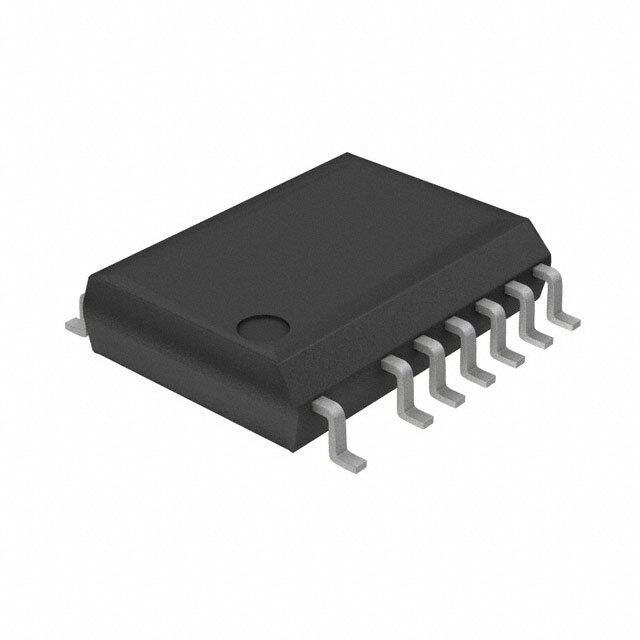
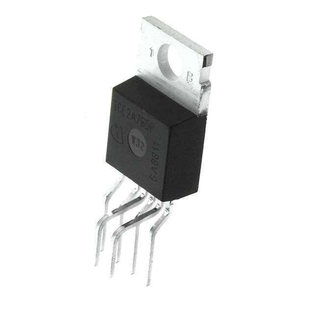
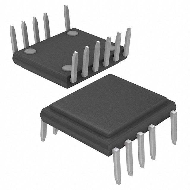
| 供应商器件封装 | 16-SO |
| 其它名称 | 497-10744-5 |
| 其它有关文件 | http://www.st.com/web/catalog/sense_power/FM142/CL1454/SC432/SS1635/PF250858?referrer=70071840 |
| 功率(W) | 20W |
| 包装 | 管件 |
| 占空比-最大 | 80 % |
| 参考设计库 | http://www.digikey.com/rdl/4294959904/4294959862/752 |
| 商标 | STMicroelectronics |
| 安装风格 | SMD/SMT |
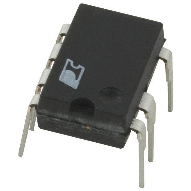
| 封装 | Tube |
| 封装/外壳 | 16-SOIC(0.154",3.90mm 宽) |
| 封装/箱体 | SOIC-16 Narrow |
| 工作温度 | -40°C ~ 150°C |
| 工作温度范围 | - 25 C to + 125 C |
| 工厂包装数量 | 50 |
| 开关频率 | 60 kHz |
| 标准包装 | 50 |
| 特色产品 | http://www.digikey.cn/product-highlights/cn/zh/stmicroelectronics-viperplus-converters/3895 |
| 电压-击穿 | 800V |
| 电压-输入 | 11.5 V ~ 23.5 V |
| 电压-输出 | - |
| 电源电流 | 0.6 mA |
| 系列 | VIPER26 |
| 输出电流 | 1 A |
| 输出端数量 | 1 Output |
| 输出隔离 | 任意一种 |
| 配用 | /product-detail/zh/STEVAL-ISA116V1/497-14476-ND/4759348 |
| 频率范围 | 54kHz ~ 66kHz |


PDF Datasheet 数据手册内容提取
VIPER26 TM Fixed frequency VIPer plus family Features ■ 800 V avalanche rugged power section ■ PWM operation with frequency jittering for low EMI SO16 narrow DIP-7 ■ Operating frequency: SO-16 – 60 kHz for L type Description – 115 kHz for H type The device is an off-line converter with an 800 V ■ Standby power < 50 mW at 265 V AC avalanche ruggedness power section, a PWM ■ Limiting current with adjustable set point controller, user defined overcurrent limit, protection against feedback network ■ On-board soft-start disconnection, hysteretic thermal protection, soft ■ Safe auto-restart after a fault condition start up and safe auto restart after any fault ■ Hysteretic thermal shutdown condition. Advance frequency jittering reduces EMI filter Application cost. Burst mode operation and the devices very low consumption both help to meet the standard ■ Auxiliary power supply for appliances set by energy saving regulations. ■ Power metering ≤ Figure 1. Typical topology (V V ) ■ LED drivers OUT DDCSon ■ SMPS for set-top boxes, DVD players and DC Input Voltage DC Output Voltage recorders - DDRRAAIINN CCOOMMPP VVIIPPEERR2266 GGNNDD VVDDDD LLIIMM FFBB Table 1. Device summary Order codes Package Packaging VIPER26LN DIP-7 Tube VIPER26HN VIPER26HD Tube VIPER26HDTR Tape and reel SO16 narrow VIPER26LD Tube VIPER26LDTR Tape and reel September 2010 Doc ID 17736 Rev 2 1/25 www.st.com 25
Contents VIPER26 Contents 1 Block diagram . . . . . . . . . . . . . . . . . . . . . . . . . . . . . . . . . . . . . . . . . . . . . . 3 2 Typical power . . . . . . . . . . . . . . . . . . . . . . . . . . . . . . . . . . . . . . . . . . . . . . . 3 3 Pin settings . . . . . . . . . . . . . . . . . . . . . . . . . . . . . . . . . . . . . . . . . . . . . . . . 4 4 Electrical data . . . . . . . . . . . . . . . . . . . . . . . . . . . . . . . . . . . . . . . . . . . . . . 5 4.1 Maximum ratings . . . . . . . . . . . . . . . . . . . . . . . . . . . . . . . . . . . . . . . . . . . . 5 4.2 Thermal data . . . . . . . . . . . . . . . . . . . . . . . . . . . . . . . . . . . . . . . . . . . . . . . 5 4.3 Electrical characteristics . . . . . . . . . . . . . . . . . . . . . . . . . . . . . . . . . . . . . . . 6 5 Typical electrical characteristics . . . . . . . . . . . . . . . . . . . . . . . . . . . . . . . 8 6 Typical circuits . . . . . . . . . . . . . . . . . . . . . . . . . . . . . . . . . . . . . . . . . . . . 10 7 Power section . . . . . . . . . . . . . . . . . . . . . . . . . . . . . . . . . . . . . . . . . . . . . 13 8 High voltage current generator . . . . . . . . . . . . . . . . . . . . . . . . . . . . . . . 13 9 Oscillator . . . . . . . . . . . . . . . . . . . . . . . . . . . . . . . . . . . . . . . . . . . . . . . . . 14 10 Soft start-up . . . . . . . . . . . . . . . . . . . . . . . . . . . . . . . . . . . . . . . . . . . . . . . 14 11 Adjustable current limit set point . . . . . . . . . . . . . . . . . . . . . . . . . . . . . 14 12 FB pin and COMP pin . . . . . . . . . . . . . . . . . . . . . . . . . . . . . . . . . . . . . . . 15 13 Burst mode . . . . . . . . . . . . . . . . . . . . . . . . . . . . . . . . . . . . . . . . . . . . . . . 16 14 Automatic auto restart after overload or short-circuit . . . . . . . . . . . . . 17 15 Open loop failure protection . . . . . . . . . . . . . . . . . . . . . . . . . . . . . . . . . 18 16 Package mechanical data . . . . . . . . . . . . . . . . . . . . . . . . . . . . . . . . . . . . 20 17 Revision history . . . . . . . . . . . . . . . . . . . . . . . . . . . . . . . . . . . . . . . . . . . 24 2/25 Doc ID 17736 Rev 2
VIPER26 Block diagram 1 Block diagram F igure 2. Block diagram 2 Typical power T able 2. Typical power 230 V 85-265 V AC AC Part number Adapter(1) Open frame(2) Adapter(1) Open frame(2) VIPER26 18 W 20 W 10 W 12 W 1. Typical continuous power in non ventilated enclosed adapter measured at 50 °C ambient. 2. Maximum practical continuous power in an open frame design at 50 °C ambient, with adequate heat sinking. Doc ID 17736 Rev 2 3/25
Pin settings VIPER26 3 Pin settings Figure 3. Connection diagram (top view) (cid:46)(cid:14)(cid:35)(cid:14) (cid:46)(cid:14)(cid:33)(cid:14) (cid:33)(cid:45)(cid:16)(cid:17)(cid:16)(cid:25)(cid:24)(cid:86)(cid:17) Note: The copper area for heat dissipation has to be designed under the DRAIN pins. Table 3. Pin description Pin n. Name Function DIP-7 SO16 Connected to the source of the internal power MOSFET and controller 1 1-2 GND ground reference. Not available for user. It can be connected to GND (pins 1-2) or left not - 4 N.A. connected. Supply voltage of the control section. This pin provides the charging current 2 5 VDD of the external capacitor. This pin allows setting the drain current limitation. The limit can be reduced 3 6 LIM by connecting an external resistor between this pin and GND. Pin left open if default drain current limitation is used. Inverting input of the internal trans conductance error amplifier. Connecting the converter output to this pin through a single resistor results in an output 4 7 FB voltage equal to the error amplifier reference voltage (See V on FB_REF Table7). An external resistors divider is required for higher output voltages. Output of the internal trans conductance error amplifier. The compensation network have to be placed between this pin and GND to achieve stability and good dynamic performance of the voltage control loop. The pin is used also 5 8 COMP to directly control the PWM with an optocoupler. The linear voltage range extends from V to V COMPL COMPH (Table7). High voltage drain pin. The built-in high voltage switched start-up bias 7,8 13-16 DRAIN current is drawn from this pin too. Pins connected to the metal frame to facilitate heat dissipation. 4/25 Doc ID 17736 Rev 2
VIPER26 Electrical data 4 Electrical data 4.1 Maximum ratings Table 4. Absolute maximum ratings Value Pin Symbol Parameter Unit (DIP-7) Min Max V 7, 8 Drain-to-source (ground) voltage 800 V DRAIN E 7, 8 Repetitive avalanche energy (limited by T = 150 °C) 5 mJ AV J I 7, 8 Repetitive avalanche current (limited by T = 150 °C) 1.5 A AR J I 7, 8 Pulse drain current (limited by T = 150 °C) 3 A DRAIN J V 5 Input pin voltage -0.3 3.5 V COMP V 4 Input pin voltage -0.3 4.8 V FB V 3 Input pin voltage -0.3 2.4 V LIM Self V 2 Supply voltage -0.3 V DD limited I 2 Input current 20 mA DD Power dissipation at T < 40 °C (DIP-7) 1 W A P TOT Power dissipation at T < 60 °C (SO16N) 1.5 W A T Operating junction temperature range -40 150 °C J T Storage temperature -55 150 °C STG 4.2 Thermal data Table 5. Thermal data Max value Symbol Parameter Unit SO16N DIP-7 Thermal resistance junction pin R 25 35 °C/W thJP (Dissipated power = 1 W) Thermal resistance junction ambient R 60 100 °C/W thJA (Dissipated power = 1 W) Thermal resistance junction ambient (1) R 50 80 °C/W thJA (Dissipated power = 1 W) 1. When mounted on a standard single side FR4 board with 100 mm2 (0.155 sq in) of Cu (35 µm thick) Doc ID 17736 Rev 2 5/25
Electrical data VIPER26 4.3 Electrical characteristics (T = -25 to 125 °C, V = 14 V (a); unless otherwise specified) J DD Table 6. P ower section Symbol Parameter Test condition Min Typ Max Unit I = 1 mA, V Break-down voltage DRAIN 800 V BVDSS V = GND, T = 25 °C COMP J V = max rating, I OFF state drain current DRAIN 60 µA OFF V = GND COMP Drain-source on state IDRAIN = 0.2 A, TJ = 25 °C 7 Ω R DS(on) resistance I = 0.2 A, T = 125 °C 14 Ω DRAIN J Effective (energy related) C V = 0 to 640 V 40 pF OSS output capacitance DRAIN Table 7. S upply section Symbol Parameter Test condition Min Typ Max Unit Voltage V Drain-source start voltage 60 80 100 V DRAIN_START Charging current during the V = 100 V to 640 V, I DRAIN -0.6 -1.8 mA DDch1 start up V = 4 V DD Charging current during the V = 100 V to 640 V, I DRAIN -7 -13 mA DDch2 autorestart V = 9 V falling edge DD V Operating voltage range 11.5 23.5 V DD V V clamp voltage I = 15 mA 23.5 V DDclamp DD DD V V start up threshold 12 13 14 V DDon DD VDD on internal high voltage V 9.5 10.5 11.5 V DDCSon current generator threshold V under voltage shutdown V DD 7 8 9 V DDoff threshold Current I Operating supply current, not FOSC = 0 kHz, 0.6 mA DD0 switching V = GND COMP V = 120 V, DRAIN 2.5 mA Operating supply current, FSW = 60 kHz I DD1 switching V = 120 V, DRAIN 3.5 mA F = 115 kHz SW Operating supply current with I V < V 0.35 mA DDoff V < V DD DDoff DD DDoff Open loop failure current V = V I DD DDclamp 4 mA DDol threshold V = 3.3 V, COMP a. Adjust V above V startup threshold before setting to 14 V DD DDon 6/25 Doc ID 17736 Rev 2
VIPER26 Electrical data Table 8. Controller section Symbol Parameter Test condition Min Typ Max Unit Error amplifier V FB reference voltage 3.2 3.3 3.4 V REF_FB I Current pull up -1 µA FB_PULL UP G Trans conductance 2 mA/V M Current setting (LIM) pin V Low level clamp voltage I = -100 µA 0.5 V LIM_LOW LIM Compensation (COMP) pin V Upper saturation limit T = 25 °C 3 V COMPH J V Burst mode threshold T = 25 °C 1 1.1 1.2 V COMPL J V Burst mode hysteresis T = 25 °C 40 mV COMPL_HYS J H ∆V / ∆I 3 V/A COMP COMP DRAIN R Dynamic resistance V = GND 15 kΩ COMP(DYN) FB Source / sink current V > 100 mV 150 µA FB I COMP Max source current V = GND, V = GND 220 µA COMP FB Current limitation I Drain current limitation I = -10 µA, V = 3.3 V, T = 25 °C 0.66 0.7 0.74 A Dlim LIM COMP J t Soft-start time 8.5 ms SS T Minimum turn ON time 480 ns ON_MIN I Burst mode current limitation V = V 145 mA Dlim_bm COMP COMPL Overload t Overload time 50 ms OVL t Restart time after fault 1 s RESTART Oscillator section VIPER26L 54 60 66 kHz F Switching frequency OSC VIPER26H 103 115 127 kHz F = 60 kHz ±4 kHz OSC F Modulation depth D F = 115 kHz ±8 kHz OSC F Modulation frequency 230 Hz M D Maximum duty cycle 70 80 % MAX Thermal shutdown T Thermal shutdown temperature 150 160 °C SD T Thermal shutdown hysteresis 30 °C HYST Doc ID 17736 Rev 2 7/25
Typical electrical characteristics VIPER26 5 Typical electrical characteristics Figure 4. I D lim vs T Figure 5. F vs T J OSC J (cid:21)(cid:15)(cid:19)(cid:19) (cid:44)(cid:39)(cid:47)(cid:44)(cid:48)(cid:18)(cid:3)(cid:44)(cid:39)(cid:47)(cid:44)(cid:48)(cid:35)(cid:21)(cid:24)(cid:38) (cid:21)(cid:15)(cid:19)(cid:19) (cid:41)(cid:50)(cid:54)(cid:38)(cid:18)(cid:3)(cid:41)(cid:50)(cid:54)(cid:38)(cid:35)(cid:21)(cid:24)(cid:38) (cid:20)(cid:15)(cid:27)(cid:19) (cid:20)(cid:15)(cid:27)(cid:19) (cid:20)(cid:15)(cid:25)(cid:19) (cid:20)(cid:15)(cid:25)(cid:19) (cid:20)(cid:15)(cid:23)(cid:19) (cid:20)(cid:15)(cid:23)(cid:19) (cid:20)(cid:15)(cid:21)(cid:19) (cid:20)(cid:15)(cid:21)(cid:19) (cid:20)(cid:15)(cid:19)(cid:19) (cid:20)(cid:15)(cid:19)(cid:19) (cid:19)(cid:15)(cid:27)(cid:19) (cid:19)(cid:15)(cid:27)(cid:19) (cid:19)(cid:15)(cid:25)(cid:19) (cid:19)(cid:15)(cid:25)(cid:19) (cid:19)(cid:15)(cid:23)(cid:19) (cid:19)(cid:15)(cid:23)(cid:19) (cid:19)(cid:15)(cid:21)(cid:19) (cid:19)(cid:15)(cid:21)(cid:19) (cid:19)(cid:15)(cid:19)(cid:19) (cid:19)(cid:15)(cid:19)(cid:19) (cid:16)(cid:24)(cid:19) (cid:19) (cid:24)(cid:19) (cid:20)(cid:19)(cid:19) (cid:20)(cid:24)(cid:19) (cid:16)(cid:24)(cid:19) (cid:19) (cid:24)(cid:19) (cid:20)(cid:19)(cid:19) (cid:20)(cid:24)(cid:19) (cid:33)(cid:45)(cid:16)(cid:17)(cid:17)(cid:20)(cid:20)(cid:86)(cid:17) (cid:33)(cid:45)(cid:16)(cid:17)(cid:17)(cid:20)(cid:21)(cid:86)(cid:17) Figure 6. V vs T Figure 7. H vs T DRAIN_START J COMP J (cid:21)(cid:15)(cid:19)(cid:19) (cid:57)(cid:39)(cid:53)(cid:36)(cid:44)(cid:49)(cid:66)(cid:54)(cid:55)(cid:36)(cid:53)(cid:55)(cid:18)(cid:3)(cid:57)(cid:39)(cid:53)(cid:36)(cid:44)(cid:49)(cid:66)(cid:54)(cid:55)(cid:36)(cid:53)(cid:55)(cid:35)(cid:21)(cid:24)(cid:38) (cid:21)(cid:15)(cid:19)(cid:19) (cid:43)(cid:38)(cid:50)(cid:48)(cid:51)(cid:3)(cid:18)(cid:3)(cid:43)(cid:38)(cid:50)(cid:48)(cid:51)(cid:35)(cid:21)(cid:24)(cid:38) (cid:20)(cid:15)(cid:27)(cid:19) (cid:20)(cid:15)(cid:27)(cid:19) (cid:20)(cid:15)(cid:25)(cid:19) (cid:20)(cid:15)(cid:25)(cid:19) (cid:20)(cid:15)(cid:23)(cid:19) (cid:20)(cid:15)(cid:23)(cid:19) (cid:20)(cid:15)(cid:21)(cid:19) (cid:20)(cid:15)(cid:21)(cid:19) (cid:20)(cid:15)(cid:19)(cid:19) (cid:20)(cid:15)(cid:19)(cid:19) (cid:19)(cid:15)(cid:27)(cid:19) (cid:19)(cid:15)(cid:27)(cid:19) (cid:19)(cid:15)(cid:25)(cid:19) (cid:19)(cid:15)(cid:25)(cid:19) (cid:19)(cid:15)(cid:23)(cid:19) (cid:19)(cid:15)(cid:23)(cid:19) (cid:19)(cid:15)(cid:21)(cid:19) (cid:19)(cid:15)(cid:21)(cid:19) (cid:19)(cid:15)(cid:19)(cid:19) (cid:19)(cid:15)(cid:19)(cid:19) (cid:16)(cid:24)(cid:19) (cid:19) (cid:24)(cid:19) (cid:20)(cid:19)(cid:19) (cid:20)(cid:24)(cid:19) (cid:16)(cid:24)(cid:19) (cid:19) (cid:24)(cid:19) (cid:20)(cid:19)(cid:19) (cid:20)(cid:24)(cid:19) (cid:33)(cid:45)(cid:16)(cid:17)(cid:17)(cid:20)(cid:22)(cid:86)(cid:17) (cid:33)(cid:45)(cid:16)(cid:17)(cid:17)(cid:20)(cid:23)(cid:86)(cid:17) Figure 8. G vs T Figure 9. V vs T M J REF_FB J (cid:21)(cid:15)(cid:19)(cid:19) (cid:42)(cid:48)(cid:3)(cid:18)(cid:3)(cid:42)(cid:48)(cid:35)(cid:21)(cid:24)(cid:38) (cid:21)(cid:15)(cid:19)(cid:19) (cid:57)(cid:53)(cid:40)(cid:41)(cid:66)(cid:41)(cid:37)(cid:3)(cid:18)(cid:3)(cid:57)(cid:53)(cid:40)(cid:66)(cid:41)(cid:37)(cid:35)(cid:21)(cid:24)(cid:38) (cid:20)(cid:15)(cid:27)(cid:19) (cid:20)(cid:15)(cid:27)(cid:19) (cid:20)(cid:15)(cid:25)(cid:19) (cid:20)(cid:15)(cid:25)(cid:19) (cid:20)(cid:15)(cid:23)(cid:19) (cid:20)(cid:15)(cid:23)(cid:19) (cid:20)(cid:15)(cid:21)(cid:19) (cid:20)(cid:15)(cid:21)(cid:19) (cid:20)(cid:15)(cid:19)(cid:19) (cid:20)(cid:15)(cid:19)(cid:19) (cid:19)(cid:15)(cid:27)(cid:19) (cid:19)(cid:15)(cid:27)(cid:19) (cid:19)(cid:15)(cid:25)(cid:19) (cid:19)(cid:15)(cid:25)(cid:19) (cid:19)(cid:15)(cid:23)(cid:19) (cid:19)(cid:15)(cid:23)(cid:19) (cid:19)(cid:15)(cid:21)(cid:19) (cid:19)(cid:15)(cid:21)(cid:19) (cid:19)(cid:15)(cid:19)(cid:19) (cid:19)(cid:15)(cid:19)(cid:19) (cid:16)(cid:24)(cid:19) (cid:19) (cid:24)(cid:19) (cid:20)(cid:19)(cid:19) (cid:20)(cid:24)(cid:19) (cid:16)(cid:24)(cid:19) (cid:19) (cid:24)(cid:19) (cid:20)(cid:19)(cid:19) (cid:20)(cid:24)(cid:19) (cid:33)(cid:45)(cid:16)(cid:17)(cid:17)(cid:20)(cid:24)(cid:86)(cid:17) (cid:33)(cid:45)(cid:16)(cid:17)(cid:17)(cid:20)(cid:25)(cid:86)(cid:17) 8/25 Doc ID 17736 Rev 2
VIPER26 Typical electrical characteristics Figure 10. I vs T Figure 11. Operating supply current COMP J (no switching) vs T J (cid:44)(cid:38)(cid:50)(cid:48)(cid:51)(cid:3)(cid:18)(cid:3)(cid:44)(cid:38)(cid:50)(cid:48)(cid:51)(cid:35)(cid:21)(cid:24)(cid:38) (cid:21)(cid:15)(cid:19)(cid:19) (cid:21)(cid:15)(cid:19)(cid:19) (cid:44)(cid:39)(cid:39)(cid:19)(cid:3)(cid:18)(cid:3)(cid:44)(cid:39)(cid:39)(cid:19)(cid:35)(cid:21)(cid:24)(cid:38) (cid:20)(cid:15)(cid:27)(cid:19) (cid:20)(cid:15)(cid:27)(cid:19) (cid:20)(cid:15)(cid:25)(cid:19) (cid:20)(cid:15)(cid:25)(cid:19) (cid:20)(cid:15)(cid:23)(cid:19) (cid:20)(cid:15)(cid:23)(cid:19) (cid:20)(cid:15)(cid:21)(cid:19) (cid:20)(cid:15)(cid:21)(cid:19) (cid:20)(cid:15)(cid:19)(cid:19) (cid:20)(cid:15)(cid:19)(cid:19) (cid:19)(cid:15)(cid:27)(cid:19) (cid:19)(cid:15)(cid:27)(cid:19) (cid:19)(cid:15)(cid:25)(cid:19) (cid:19)(cid:15)(cid:25)(cid:19) (cid:19)(cid:15)(cid:23)(cid:19) (cid:19)(cid:15)(cid:23)(cid:19) (cid:19)(cid:15)(cid:21)(cid:19) (cid:19)(cid:15)(cid:21)(cid:19) (cid:19)(cid:15)(cid:19)(cid:19) (cid:19)(cid:15)(cid:19)(cid:19) (cid:16)(cid:24)(cid:19) (cid:19) (cid:24)(cid:19) (cid:20)(cid:19)(cid:19) (cid:20)(cid:24)(cid:19) (cid:16)(cid:24)(cid:19) (cid:19) (cid:24)(cid:19) (cid:20)(cid:19)(cid:19) (cid:20)(cid:24)(cid:19) (cid:33)(cid:45)(cid:16)(cid:17)(cid:17)(cid:21)(cid:16)(cid:86)(cid:17) (cid:33)(cid:45)(cid:16)(cid:17)(cid:17)(cid:21)(cid:17)(cid:86)(cid:17) Figure 12. Operating supply current Figure 13. IDlim vs R LIM (switching) vs T J (cid:44)(cid:39)(cid:39)(cid:20)(cid:3)(cid:18)(cid:3)(cid:44)(cid:39)(cid:39)(cid:20)(cid:35)(cid:21)(cid:24)(cid:38) (cid:21)(cid:15)(cid:19)(cid:19) (cid:20)(cid:15)(cid:21)(cid:19) (cid:44)(cid:39)(cid:47)(cid:44)(cid:48)(cid:18)(cid:3)(cid:44)(cid:39)(cid:47)(cid:44)(cid:48)(cid:35)(cid:20)(cid:19)(cid:19)(cid:46)(cid:50)(cid:75)(cid:80) (cid:20)(cid:15)(cid:27)(cid:19) (cid:20)(cid:15)(cid:25)(cid:19) (cid:20)(cid:15)(cid:19)(cid:19) (cid:20)(cid:15)(cid:23)(cid:19) (cid:19)(cid:15)(cid:27)(cid:19) (cid:20)(cid:15)(cid:21)(cid:19) (cid:20)(cid:15)(cid:19)(cid:19) (cid:19)(cid:15)(cid:25)(cid:19) (cid:19)(cid:15)(cid:27)(cid:19) (cid:19)(cid:15)(cid:25)(cid:19) (cid:19)(cid:15)(cid:23)(cid:19) (cid:19)(cid:15)(cid:23)(cid:19) (cid:19)(cid:15)(cid:21)(cid:19) (cid:19)(cid:15)(cid:21)(cid:19) (cid:19)(cid:15)(cid:19)(cid:19) (cid:19)(cid:15)(cid:19)(cid:19) (cid:16)(cid:24)(cid:19) (cid:19) (cid:24)(cid:19) (cid:20)(cid:19)(cid:19) (cid:20)(cid:24)(cid:19) (cid:19) (cid:21)(cid:19) (cid:23)(cid:19) (cid:25)(cid:19) (cid:27)(cid:19) (cid:20)(cid:19)(cid:19) (cid:20)(cid:21)(cid:19) (cid:33)(cid:45)(cid:16)(cid:17)(cid:17)(cid:21)(cid:18)(cid:86)(cid:17) (cid:33)(cid:45)(cid:16)(cid:17)(cid:17)(cid:21)(cid:19)(cid:86)(cid:17) Figure 14. Power MOSFET on-resistance vs T Figure 15. Power MOSFET break down voltage J vs T J (cid:24)(cid:15)(cid:19)(cid:19) (cid:53)(cid:39)(cid:54)(cid:50)(cid:49)(cid:18)(cid:3)(cid:53)(cid:39)(cid:54)(cid:50)(cid:49)(cid:35)(cid:21)(cid:24)(cid:38) (cid:21)(cid:15)(cid:19)(cid:19) (cid:37)(cid:57)(cid:39)(cid:54)(cid:54)(cid:18)(cid:3)(cid:37)(cid:57)(cid:39)(cid:54)(cid:54)(cid:35)(cid:21)(cid:24)(cid:38) (cid:23)(cid:15)(cid:24)(cid:19) (cid:20)(cid:15)(cid:27)(cid:19) (cid:23)(cid:15)(cid:19)(cid:19) (cid:20)(cid:15)(cid:25)(cid:19) (cid:22)(cid:15)(cid:24)(cid:19) (cid:20)(cid:15)(cid:23)(cid:19) (cid:22)(cid:15)(cid:19)(cid:19) (cid:20)(cid:15)(cid:21)(cid:19) (cid:21)(cid:15)(cid:24)(cid:19) (cid:20)(cid:15)(cid:19)(cid:19) (cid:21)(cid:15)(cid:19)(cid:19) (cid:19)(cid:15)(cid:27)(cid:19) (cid:20)(cid:15)(cid:24)(cid:19) (cid:19)(cid:15)(cid:25)(cid:19) (cid:20)(cid:15)(cid:19)(cid:19) (cid:19)(cid:15)(cid:23)(cid:19) (cid:19)(cid:15)(cid:24)(cid:19) (cid:19)(cid:15)(cid:21)(cid:19) (cid:19)(cid:15)(cid:19)(cid:19) (cid:19)(cid:15)(cid:19)(cid:19) (cid:16)(cid:24)(cid:19) (cid:19) (cid:24)(cid:19) (cid:20)(cid:19)(cid:19) (cid:20)(cid:24)(cid:19) (cid:16)(cid:24)(cid:19) (cid:19) (cid:24)(cid:19) (cid:20)(cid:19)(cid:19) (cid:20)(cid:24)(cid:19) (cid:33)(cid:45)(cid:16)(cid:18)(cid:19)(cid:25)(cid:23)(cid:86)(cid:17) (cid:33)(cid:45)(cid:16)(cid:18)(cid:19)(cid:25)(cid:24)(cid:86)(cid:17) Doc ID 17736 Rev 2 9/25
Typical circuits VIPER26 Figure 16. Thermal shutdown V DD V DDon V DDCSon V DDoff I time DRAIN time T J T SD T -T SD HYST time Normal operation Shut down after over temperature Normal operation 6 Typical circuits Figure 17. Buck converter (V >V ) OUT DDCSon (cid:36)(cid:17) (cid:50)(cid:70)(cid:66)(cid:17) (cid:33)(cid:35)(cid:0)(cid:41)(cid:46) (cid:36)(cid:17) (cid:50)(cid:16) (cid:44)(cid:17) (cid:54)(cid:41)(cid:48)(cid:37)(cid:50)(cid:18)(cid:22) (cid:54)(cid:36)(cid:36) (cid:36)(cid:50)(cid:33)(cid:41)(cid:46) (cid:36)(cid:18) (cid:38)(cid:34) (cid:50)(cid:70)(cid:66)(cid:18) (cid:35)(cid:20) (cid:35)(cid:17) (cid:35)(cid:47)(cid:46)(cid:52)(cid:50)(cid:47)(cid:44) (cid:35)(cid:18) (cid:35)(cid:19) (cid:35)(cid:70)(cid:66) (cid:35)(cid:47)(cid:45)(cid:48) (cid:44)(cid:41)(cid:45) (cid:39)(cid:46)(cid:36) (cid:50)(cid:67)(cid:79)(cid:77)(cid:80) (cid:50)(cid:44)(cid:41)(cid:45) (cid:8)(cid:79)(cid:80)(cid:84)(cid:73)(cid:79)(cid:78)(cid:65)(cid:76)(cid:9) (cid:35)(cid:67)(cid:79)(cid:77)(cid:80) (cid:44)(cid:79)(cid:85)(cid:84) (cid:54)(cid:47)(cid:53)(cid:52) (cid:36)(cid:79)(cid:85)(cid:84) (cid:35)(cid:79)(cid:85)(cid:84) (cid:39)(cid:50)(cid:47)(cid:53)(cid:46)(cid:36) (cid:39)(cid:50)(cid:47)(cid:53)(cid:46)(cid:36) (cid:33)(cid:45)(cid:16)(cid:17)(cid:17)(cid:25)(cid:20)(cid:86)(cid:17) 10/25 Doc ID 17736 Rev 2
VIPER26 Typical circuits Figure 18. Fly-back converter (isolated) (cid:33)(cid:35)(cid:0)(cid:41)(cid:46) (cid:50)(cid:17) (cid:44)(cid:17) (cid:52)(cid:17) (cid:21) (cid:35)(cid:67)(cid:76)(cid:50)(cid:67)(cid:76) (cid:36)(cid:16) (cid:36)(cid:18) (cid:13) (cid:11) (cid:23) (cid:54)(cid:79)(cid:85)(cid:84) (cid:36)(cid:17) (cid:33)(cid:35)(cid:0)(cid:41)(cid:46) (cid:50)(cid:19) (cid:36)(cid:19) (cid:20) (cid:11)(cid:35)(cid:25) (cid:17) (cid:24) (cid:13) (cid:54)(cid:41)(cid:48)(cid:37)(cid:50)(cid:18)(cid:22) (cid:18) (cid:54)(cid:36)(cid:36) (cid:36)(cid:50)(cid:33)(cid:41)(cid:46) (cid:35)(cid:17)(cid:18) (cid:50)(cid:24) (cid:35)(cid:17) (cid:11) (cid:35)(cid:18) (cid:11) (cid:38)(cid:34) (cid:35)(cid:47)(cid:46)(cid:52)(cid:50)(cid:47)(cid:44) (cid:50)(cid:82)(cid:69)(cid:70)(cid:17) (cid:35)(cid:47)(cid:45)(cid:48) (cid:44)(cid:41)(cid:45) (cid:39)(cid:46)(cid:36) (cid:35)(cid:20) (cid:11) (cid:47)(cid:48)(cid:52)(cid:47) (cid:50)(cid:25) (cid:50)(cid:23) (cid:35)(cid:24) (cid:50)(cid:17)(cid:16) (cid:50)(cid:44)(cid:41)(cid:45) (cid:35)(cid:23) (cid:41)(cid:35)(cid:18) (cid:35)(cid:17)(cid:17) (cid:50)(cid:82)(cid:69)(cid:70)(cid:18) (cid:39)(cid:50)(cid:47)(cid:53)(cid:46)(cid:36)(cid:17) (cid:39)(cid:50)(cid:47)(cid:53)(cid:46)(cid:36)(cid:18) (cid:0) (cid:33)(cid:45)(cid:16)(cid:17)(cid:17)(cid:25)(cid:21)(cid:86)(cid:17) Figure 19. Flyback converter (primary regulation) (cid:33)(cid:45)(cid:16)(cid:17)(cid:17)(cid:25)(cid:22)(cid:86)(cid:17) Doc ID 17736 Rev 2 11/25
Typical circuits VIPER26 Figure 20. Flyback converter (non isolated, V mV ) OUT DDCSon (cid:33)(cid:35)(cid:0)(cid:41)(cid:46) (cid:50)(cid:73)(cid:78) (cid:44)(cid:17) (cid:17) (cid:22)(cid:22) (cid:36)(cid:73)(cid:78) (cid:18) (cid:13) (cid:11) (cid:20) (cid:35)(cid:18) (cid:11) (cid:35)(cid:19) (cid:11) (cid:50)(cid:67)(cid:76) (cid:35)(cid:67)(cid:76) (cid:36)(cid:79)(cid:85)(cid:84) (cid:54)(cid:47)(cid:53)(cid:52) (cid:33)(cid:35)(cid:0)(cid:41)(cid:46) (cid:17)(cid:18) (cid:19) (cid:36)(cid:17) (cid:20) (cid:11) (cid:35)(cid:79)(cid:85)(cid:84) (cid:17)(cid:16) (cid:36)(cid:65)(cid:85)(cid:88) (cid:54)(cid:41)(cid:48)(cid:37)(cid:50)(cid:18)(cid:22) (cid:50)(cid:70)(cid:66)(cid:17) (cid:54)(cid:36)(cid:36) (cid:36)(cid:50)(cid:33)(cid:41)(cid:46) (cid:38)(cid:34) (cid:35)(cid:47)(cid:46)(cid:52)(cid:50)(cid:47)(cid:44) (cid:50)(cid:70)(cid:66)(cid:18) (cid:35)(cid:17) (cid:35)(cid:47)(cid:45)(cid:48) (cid:44)(cid:41)(cid:45) (cid:39)(cid:46)(cid:36) (cid:50)(cid:67)(cid:79)(cid:77)(cid:80)(cid:17) (cid:35)(cid:67)(cid:79)(cid:77)(cid:80)(cid:18) (cid:50)(cid:44)(cid:41)(cid:45) (cid:8)(cid:79)(cid:80)(cid:84)(cid:73)(cid:79)(cid:78)(cid:65)(cid:76)(cid:9) (cid:35)(cid:67)(cid:79)(cid:77)(cid:80)(cid:17) (cid:33)(cid:45)(cid:16)(cid:17)(cid:17)(cid:25)(cid:23)(cid:86)(cid:17) Figure 21. Flyback converter (non isolated, V [V ) OUT DDCSon 12/25 Doc ID 17736 Rev 2
VIPER26 Power section 7 Power section The power section is implemented with an n-channel power MOSFET with a breakdown voltage of 800 V min. and a typical R of 7 Ω. It includes a SenseFET structure to allow DS(on) a virtually lossless current sensing and the thermal sensor. The gate driver of the power MOSFET is designed to supply a controlled gate current during both turn-ON and turn-OFF in order to minimize common mode EMI. During UVLO conditions, an internal pull-down circuit holds the gate low in order to ensure that the power MOSFET cannot be turned ON accidentally. 8 High voltage current generator The high voltage current generator is supplied by the DRAIN pin. At the first start up of the converter, it is enabled when the voltage across the input bulk capacitor reaches the V threshold, sourcing the I current (see Table7 on page6); as the V DRAIN_START DDch1 DD voltage reaches the V start-up threshold, the power section starts switching and the DDon high voltage current generator is turned OFF. The VIPer26 is powered by the external source. After the start-up, the auxiliary winding or the diode connected to the output voltage have to power the VDD capacitor with voltage higher than V threshold (see Table7 DDCSon on page6). During the switching, the internal current source is disabled and the consumptions are minimized. In case of fault the switching is stopped and the device is self biased by the internal high voltage current source; it is activated between the levels V DDCSon and V delivering the current I to the V capacitor during the MOSFET off time, DDon DDch2 DD see Figure22 on page13. At converter power-down, the V voltage drops and the converter activity stops as it falls DD below V threshold (see Table7 on page6). DDoff Figure 22. Power on and power off V IN VIN< VDRAIN_START HV startup is no more activated V DRAIN_START VDD regulation is lost here time V DDon V DDCSon V DDoff VDRAIN time I DD time I DDch2 I DDch1 time Power-on Normal operation Power-off Doc ID 17736 Rev 2 13/25
Oscillator VIPER26 9 Oscillator The switching frequency is internally fixed at 60 kHz (VIPER26LN or LD) or 115 kHz (VIPER26HN or HD). In both cases the switching frequency is modulated by approximately ±4 kHz (60 kHz version) or ±8 kHz (115 kHz version) at 230 Hz (typical) rate, so that the resulting spread- spectrum action distributes the energy of each harmonic of the switching frequency over a number of sideband harmonics having the same energy on the whole but smaller amplitudes. 10 Soft start-up During the converters' start-up phase, the soft-start function progressively increases the cycle-by-cycle drain current limit, up to the default value I . By this way the drain current is Dlim further limited and the output voltage is progressively increased reducing the stress on the secondary diode. The soft-start time is internally fixed to t , see typical value on Table8 on SS page7, and the function is activated for any attempt of converter start-up and after a fault event. This function helps prevent transformers' saturation during start-up and short-circuit. 11 Adjustable current limit set point The VIPer26 includes a current mode PWM controller: cycle by cycle the drain current is sensed through the integrated resistor R and the voltage is applied to the non SENSE inverting input of the PWM comparator, see Figure2 on page3. As soon as the sensed voltage is equal to the voltage derived from the COMP pin, the power MOSFET is switched OFF. In parallel with the PWM operations, the comparator OCP, see Figure2 on page3, checks the level of the drain current and switch OFF the power MOSFET in case the current is higher than the threshold I , see Table8 on page7. Dlim The level of the drain current limit, I , can be reduced depending from the sunk current Dlim from the pin LIM. The resistor R , between LIM and GND pins, fixes the current sunk and LIM than the level of the current limit, I , see Figure13 on page9. Dlim When the LIM pin is left open or if the R has an high value (i.e. > 80 kΩ) the current limit LIM is fixed to its default value, I , as reported on Table8 on page7. Dlim 14/25 Doc ID 17736 Rev 2
VIPER26 FB pin and COMP pin 12 FB pin and COMP pin The device can be used both in non-isolated and in isolated topology. In case of non- isolated topology, the feedback signal from the output voltage is applied directly to the FB pin as inverting input of the internal error amplifier having the reference voltage, V REF_FB, see the Table8 on page7. The output of the error amplifier sources and sinks the current, I , respectively to and COMP from the compensation network connected on the COMP pin. This signal is then compared, in the PWM comparator, with the signal coming from the SenseFET; the power MOSFET is switched off when the two values are the same on cycle by cycle basis. See the Figure2 on page3 and the Figure23 on page15. When the power supply output voltage is equal to the error amplifier reference voltage, V , a single resistor has to be connected from the output to the FB pin. For higher REF_FB output voltages the external resistor divider is needed. If the voltage on FB pin is accidentally left floating, an internal pull-up protects the controller. The output of the error amplifier is externally accessible through the COMP pin and it’s used for the loop compensation: usually an RC network. As reported on Figure23 on page15, in case of isolated power supply, the internal error amplifier has to be disabled (FB pin shorted to GND). In this case an internal resistor is connected between an internal reference voltage and the COMP pin, see the Figure23 on page15. The current loop has to be closed on the COMP pin through the opto-transistor in parallel with the compensation network. The V dynamics ranges is between V COMP COMPL and V as reported on Figure24 on page16. COMPH When the voltage V drops below the voltage threshold V , the converter enters COMP COMPL burst mode, see Section13 on page 16. When the voltage V rises above the V threshold, the peak drain current will COMP COMPH reach its limit, as well as the deliverable output power Figure 23. Feedback circuit Wswitithcohu ot pIseonla &ti oEn/:A enabled VREF With Isolation: RCOMP VCOMPL PWM stop switch closed & E/A disabled + VOUT SW - BUS FB - from RSENSE RH VREF_FB +E/A + to PWM Isolation nR - No RL Isolation R COMP Doc ID 17736 Rev 2 15/25
Burst mode VIPER26 Figure 24. COMP pin voltage versus I DLIM (cid:3) (cid:44)(cid:39)(cid:53)(cid:36)(cid:44)(cid:49) (cid:44) (cid:39)(cid:79)(cid:76)(cid:80) (cid:44) (cid:39)(cid:79)(cid:76)(cid:80)(cid:66)(cid:69)(cid:80) (cid:57)(cid:38)(cid:50)(cid:48)(cid:51) (cid:57) (cid:57) (cid:38)(cid:50)(cid:48)(cid:51)(cid:47) (cid:38)(cid:50)(cid:48)(cid:51)(cid:43) (cid:33)(cid:45)(cid:16)(cid:17)(cid:16)(cid:25)(cid:21)(cid:86)(cid:17) 13 Burst mode When the voltage V drops below the threshold, V , the power MOSFET is kept in COMP COMPL OFF state and the consumption is reduced to I current, as reported on Table7 on DD0 page6. As reaction at the energy delivery stop, the V voltage increases and as soon COMP as it exceeds the threshold V + V , the converter starts switching again with COMPL COMPL_HYS consumption level equal to I current. This ON-OFF operation mode, referred to as “burst DD1 mode” and reported on Figure25 on page16, reduces the average frequency, which can go down even to a few hundreds hertz, thus minimizing all frequency-related losses and making it easier to comply with energy saving regulations. During the burst mode, the drain current limit is reduced to the value I (reported on Table8 on page7) in order to Dlim_bm avoid the audible noise issue. Figure 25. Load-dependent operating modes: timing diagrams V COMP VCOMPL+VCOMPL_HYS VCOMPL time I DD IDD1 IDD0 I time DRAIN IDlim_bm time Burst Mode 16/25 Doc ID 17736 Rev 2
VIPER26 Automatic auto restart after overload or short-circuit 14 Automatic auto restart after overload or short-circuit The overload protection is implemented in automatic way using the integrated up-down counter. Every cycle, it is incremented or decremented depending if the current logic detects the limit condition or not. The limit condition is the peak drain current, I reported on Dlim , Table8 on page7 or the one set by the user through the R resistor, as reported in LIM Figure13 on page9. After the reset of the counter, if the peak drain current is continuously equal to the level I , Dlim the counter will be incremented till the fixed time, t , after that will be disabled the power OVL MOSFET switch ON. It will be activated again, through the soft start, after the t time, RESTART see the Figure26 on page17 and the mentioned time values on Table8 on page7. In case of overload or short-circuit event, the power MOSFET switching will be stopped after a time that depends from the counter and that can be as maximum equal to t . The OVL protection will occur in the same way until the overload condition is removed, see Figure26 on page17. This protection ensures restart attempts of the converter with low repetition rate, so that it works safely with extremely low power throughput and avoiding the IC overheating in case of repeated overload events. If the overload is removed before the protection tripping, the counter will be decremented cycle by cycle down to zero and the IC will not be stopped. Figure 26. Timing diagram: OLP sequence SHORT CIRCUIT SHORT CIRCUIT V OCCURS HERE REMOVED HERE DD V DDon V DDCSon I time DRAIN I Dlim_bm t t time t1* tRESTART OVL tRESTART OVL tRESTART t t t SS SS SS * The timet can be lower or equal to the timet 1 OVL Doc ID 17736 Rev 2 17/25
Open loop failure protection VIPER26 15 Open loop failure protection In case the power supply is built in fly-back topology and the VIPer26 is supplied by an auxiliary winding, as shown in Figure27 on page18 and Figure28 on page19, the converter is protected against feedback loop failure or accidental disconnections of the winding. The following description is applicable for the schematics of Figure27 on page18 and Figure28 on page19, respectively the non-isolated fly-back and the isolated fly-back. If R is opened or R is shorted, the VIPer26 works at its drain current limitation. The output H L voltage, V , will increase and so the auxiliary voltage, V , which is coupled with the OUT AUX output through the secondary-to-auxiliary turns ratio. As the auxiliary voltage increases up to the internal V active clamp, V (the value is DD DDclamp reported on Table8 on page7) and the clamp current injected on VDD pin exceeds the latch threshold, I (the value is reported on Table8 on page7), a fault signal is internally DDol generated. In order to distinguish an actual malfunction from a bad auxiliary winding design, both the above conditions (drain current equal to the drain current limitation and current higher than I through VDD clamp) have to be verified to reveal the fault. DDol If R is opened or R is shorted, the output voltage, V , will be clamped to the reference L H OUT voltage V (in case of non isolated fly-back) or to the external TL voltage reference (in REF_FB case of isolated fly-back). Figure 27. FB pin connection for non-isolated fly-back (cid:50)(cid:33)(cid:53)(cid:56) (cid:36)(cid:33)(cid:53)(cid:56) (cid:35)(cid:54)(cid:36)(cid:36) (cid:54)(cid:33)(cid:53)(cid:56) (cid:54)(cid:36)(cid:36) (cid:54)(cid:47)(cid:53)(cid:52) (cid:54)(cid:35)(cid:47)(cid:45)(cid:48)(cid:44) (cid:48)(cid:55)(cid:45)(cid:0)(cid:83)(cid:84)(cid:79)(cid:80) (cid:11) (cid:13) (cid:50)(cid:40) (cid:34)(cid:53)(cid:51) (cid:38)(cid:34) (cid:13) (cid:70)(cid:82)(cid:79)(cid:77)(cid:0)(cid:50)(cid:51)(cid:37)(cid:46)(cid:51)(cid:37) (cid:37)(cid:15)(cid:33) (cid:0)(cid:50)(cid:44) (cid:54)(cid:50)(cid:37)(cid:38)(cid:63)(cid:38)(cid:34) (cid:11) (cid:84)(cid:79)(cid:0)(cid:48)(cid:55)(cid:45) (cid:78)(cid:50) (cid:11) (cid:13) (cid:50) (cid:35)(cid:47)(cid:45)(cid:48) (cid:50)(cid:83) (cid:35)(cid:80) (cid:35)(cid:83) (cid:0) 18/25 Doc ID 17736 Rev 2
VIPER26 Open loop failure protection Figure 28. FB pin connection for isolated fly-back (cid:50)(cid:33)(cid:53)(cid:56) (cid:36)(cid:33)(cid:53)(cid:56) (cid:35)(cid:54)(cid:36)(cid:36) (cid:54)(cid:33)(cid:53)(cid:56) (cid:54)(cid:50)(cid:37)(cid:38)(cid:63)(cid:38)(cid:34) (cid:50)(cid:67)(cid:79)(cid:77)(cid:80) (cid:54)(cid:35)(cid:47)(cid:45)(cid:48)(cid:44) (cid:48)(cid:55)(cid:45)(cid:0)(cid:83)(cid:84)(cid:79)(cid:80) (cid:11) (cid:51)(cid:55) (cid:13) (cid:34)(cid:53)(cid:51) (cid:38)(cid:34) (cid:36)(cid:73)(cid:83)(cid:65)(cid:66)(cid:76)(cid:69)(cid:13)(cid:68) (cid:70)(cid:82)(cid:79)(cid:77)(cid:0)(cid:50)(cid:51)(cid:37)(cid:46)(cid:51)(cid:37)(cid:0) (cid:54)(cid:47)(cid:53)(cid:52) (cid:37)(cid:15)(cid:33) (cid:11) (cid:54)(cid:50)(cid:37)(cid:38)(cid:63)(cid:38)(cid:34) (cid:84)(cid:79)(cid:0)(cid:48)(cid:55)(cid:45) (cid:78)(cid:50) (cid:11) (cid:13) (cid:50) (cid:50)(cid:79)(cid:80)(cid:84)(cid:79) (cid:50)(cid:40) (cid:35)(cid:47)(cid:45)(cid:48) (cid:50)(cid:19) (cid:53)(cid:21) (cid:50)(cid:67) (cid:35)(cid:67) (cid:35)(cid:67)(cid:79)(cid:77)(cid:80) (cid:52)(cid:44) (cid:50)(cid:44) (cid:13) Doc ID 17736 Rev 2 19/25
Package mechanical data VIPER26 16 Package mechanical data In order to meet environmental requirements, ST offers these devices in different grades of ECOPACK® packages, depending on their level of environmental compliance. ECOPACK® specifications, grade definitions and product status are available at: www.st.com. ECOPACK® is an ST trademark. T able 9. DIP-7 mechanical data mm Dim. Typ Min Max A 5.33 A1 0.38 A2 3.30 2.92 4.95 b 0.46 0.36 0.56 b2 1.52 1.14 1.78 c 0.25 0.20 0.36 D 9.27 9.02 10.16 E 7.87 7.62 8.26 E1 6.35 6.10 7.11 e 2.54 eA 7.62 eB 10.92 L 3.30 2.92 3.81 M 2.508 N 0.50 0.40 0.60 N1 0.60 O 0.548 20/25 Doc ID 17736 Rev 2
VIPER26 Package mechanical data Figure 29. DIP-7 package dimensions Doc ID 17736 Rev 2 21/25
Package mechanical data VIPER26 T able 10. SO16N mechanical data mm Dim. Min Typ Max A 1.75 A1 0.1 0.25 A2 1.25 b 0.31 0.51 c 0.17 0.25 D 9.8 9.9 10 E 5.8 6 6.2 E1 3.8 3.9 4 e 1.27 h 0.25 0.5 L 0.4 1.27 k 0 8 ccc 0.1 22/25 Doc ID 17736 Rev 2
VIPER26 Package mechanical data Figure 30. SO16N package dimensions Doc ID 17736 Rev 2 23/25
Revision history VIPER26 17 Revision history T able 11. Document revision history Date Revision Changes 26-Aug-2010 1 Initial release. 01-Sep-2010 2 Updated Figure30 on page23. 24/25 Doc ID 17736 Rev 2
VIPER26 Please Read Carefully: Information in this document is provided solely in connection with ST products. STMicroelectronics NV and its subsidiaries (“ST”) reserve the right to make changes, corrections, modifications or improvements, to this document, and the products and services described herein at any time, without notice. All ST products are sold pursuant to ST’s terms and conditions of sale. Purchasers are solely responsible for the choice, selection and use of the ST products and services described herein, and ST assumes no liability whatsoever relating to the choice, selection or use of the ST products and services described herein. No license, express or implied, by estoppel or otherwise, to any intellectual property rights is granted under this document. If any part of this document refers to any third party products or services it shall not be deemed a license grant by ST for the use of such third party products or services, or any intellectual property contained therein or considered as a warranty covering the use in any manner whatsoever of such third party products or services or any intellectual property contained therein. UNLESS OTHERWISE SET FORTH IN ST’S TERMS AND CONDITIONS OF SALE ST DISCLAIMS ANY EXPRESS OR IMPLIED WARRANTY WITH RESPECT TO THE USE AND/OR SALE OF ST PRODUCTS INCLUDING WITHOUT LIMITATION IMPLIED WARRANTIES OF MERCHANTABILITY, FITNESS FOR A PARTICULAR PURPOSE (AND THEIR EQUIVALENTS UNDER THE LAWS OF ANY JURISDICTION), OR INFRINGEMENT OF ANY PATENT, COPYRIGHT OR OTHER INTELLECTUAL PROPERTY RIGHT. UNLESS EXPRESSLY APPROVED IN WRITING BY AN AUTHORIZED ST REPRESENTATIVE, ST PRODUCTS ARE NOT RECOMMENDED, AUTHORIZED OR WARRANTED FOR USE IN MILITARY, AIR CRAFT, SPACE, LIFE SAVING, OR LIFE SUSTAINING APPLICATIONS, NOR IN PRODUCTS OR SYSTEMS WHERE FAILURE OR MALFUNCTION MAY RESULT IN PERSONAL INJURY, DEATH, OR SEVERE PROPERTY OR ENVIRONMENTAL DAMAGE. ST PRODUCTS WHICH ARE NOT SPECIFIED AS "AUTOMOTIVE GRADE" MAY ONLY BE USED IN AUTOMOTIVE APPLICATIONS AT USER’S OWN RISK. Resale of ST products with provisions different from the statements and/or technical features set forth in this document shall immediately void any warranty granted by ST for the ST product or service described herein and shall not create or extend in any manner whatsoever, any liability of ST. ST and the ST logo are trademarks or registered trademarks of ST in various countries. Information in this document supersedes and replaces all information previously supplied. The ST logo is a registered trademark of STMicroelectronics. All other names are the property of their respective owners. © 2010 STMicroelectronics - All rights reserved STMicroelectronics group of companies Australia - Belgium - Brazil - Canada - China - Czech Republic - Finland - France - Germany - Hong Kong - India - Israel - Italy - Japan - Malaysia - Malta - Morocco - Philippines - Singapore - Spain - Sweden - Switzerland - United Kingdom - United States of America www.st.com Doc ID 17736 Rev 2 25/25
Mouser Electronics Authorized Distributor Click to View Pricing, Inventory, Delivery & Lifecycle Information: S TMicroelectronics: VIPER26HDTR VIPER26LDTR VIPER26HD VIPER26HN VIPER26LD VIPER26LN VIPER265KDTR VIPER267KDTR