ICGOO在线商城 > 集成电路(IC) > PMIC - V/F 和 F/V 转换器 > VFC32KP
 Datasheet下载
- 型号: VFC32KP
- 制造商: Texas Instruments
- 库位|库存: xxxx|xxxx
- 要求:
| 数量阶梯 | 香港交货 | 国内含税 |
| +xxxx | $xxxx | ¥xxxx |
查看当月历史价格
查看今年历史价格
VFC32KP产品简介:
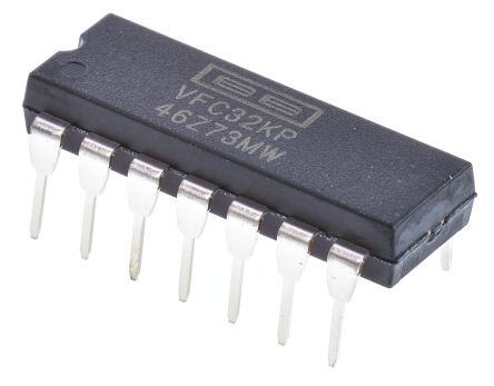
ICGOO电子元器件商城为您提供VFC32KP由Texas Instruments设计生产,在icgoo商城现货销售,并且可以通过原厂、代理商等渠道进行代购。 VFC32KP价格参考¥55.35-¥92.74。Texas InstrumentsVFC32KP封装/规格:PMIC - V/F 和 F/V 转换器, Volt to Frequency and Frequency to Volt Converter IC 100kHz ±0.05% 14-PDIP。您可以下载VFC32KP参考资料、Datasheet数据手册功能说明书,资料中有VFC32KP 详细功能的应用电路图电压和使用方法及教程。
VFC32KP是德州仪器(Texas Instruments)推出的一款高精度电压-频率(V/F)和频率-电压(F/V)转换器,属于PMIC中的信号转换类器件。该芯片广泛应用于需要将模拟信号与数字信号相互转换的工业与测量系统中。

典型应用场景包括:工业过程控制中的模拟信号数字化传输,例如将温度、压力、流量等传感器输出的4-20mA或0-10V信号转换为频率信号,便于长距离、抗干扰能力强的传输;在数据采集系统中,VFC32KP可将缓慢变化的直流信号转换为脉冲频率信号,由微控制器或计数器进行精确测量,提高系统的分辨率和稳定性;此外,在电机转速测量、电源监控、电能计量等领域,也可利用其F/V功能将频率信号(如来自转速传感器的脉冲)转换为标准电压信号供记录或显示。

VFC32KP具有高线性度、宽动态范围和良好的温度稳定性,适合对精度要求较高的场合。其DIP-8封装也便于在测试设备和原型设计中使用。总之,该器件适用于各类需要高精度模数转换接口但无需高速采样的工业自动化、仪器仪表和监控系统中。
| 参数 | 数值 |
| 产品目录 | 集成电路 (IC)半导体 |
| 描述 | IC V/F AND F/V CONVERTER 14 DIP电压频率转换及频率电压转换 VOLTAGE-TO-FREQUENCY CONVERTER |
| 产品分类 | |
| 品牌 | Texas Instruments |
| 产品手册 | |
| 产品图片 |
|
| rohs | 符合RoHS无铅 / 符合限制有害物质指令(RoHS)规范要求 |
| 产品系列 | 数据转换器IC,电压频率转换及频率电压转换,Texas Instruments VFC32KP- |
| 数据手册 | http://www.ti.com/lit/pdf/sbvs015 |
| 产品型号 | VFC32KP |
| 产品目录页面 | |
| 产品种类 | 电压频率转换及频率电压转换 |
| 供应商器件封装 | 14-PDIP |
| 全标度频率 | 100 kHz |
| 包装 | 管件 |
| 商标 | Texas Instruments |
| 安装类型 | 通孔 |
| 安装风格 | Through Hole |
| 封装 | Tube |
| 封装/外壳 | 14-DIP(0.300",7.62mm) |
| 封装/箱体 | PDIP-14 |
| 工厂包装数量 | 25 |
| 最大工作温度 | + 70 C |
| 最小工作温度 | 0 C |
| 标准包装 | 25 |
| 满刻度 | ±75ppm/°C |
| 类型 | 电压到频率和频率到电压 |
| 系列 | VFC32 |
| 线性度 | ±0.05% |
| 线性误差 | +/- 0.05 % FSR |
| 频率-最大值 | 100kHz |


- 商务部:美国ITC正式对集成电路等产品启动337调查
- 曝三星4nm工艺存在良率问题 高通将骁龙8 Gen1或转产台积电
- 太阳诱电将投资9.5亿元在常州建新厂生产MLCC 预计2023年完工
- 英特尔发布欧洲新工厂建设计划 深化IDM 2.0 战略
- 台积电先进制程称霸业界 有大客户加持明年业绩稳了
- 达到5530亿美元!SIA预计今年全球半导体销售额将创下新高
- 英特尔拟将自动驾驶子公司Mobileye上市 估值或超500亿美元
- 三星加码芯片和SET,合并消费电子和移动部门,撤换高东真等 CEO
- 三星电子宣布重大人事变动 还合并消费电子和移动部门
- 海关总署:前11个月进口集成电路产品价值2.52万亿元 增长14.8%


PDF Datasheet 数据手册内容提取
VFC32 ® Voltage-to-Frequency and Frequency-to-Voltage CONVERTER FEATURES DESCRIPTION l OPERATION UP TO 500kHz The VFC32 voltage-to-frequency converter provides l EXCELLENT LINEARITY an output frequency accurately proportional to its – 0.01% max at 10kHz FS input voltage. The digital open-collector frequency – 0.05% max at 100kHz FS output is compatible with all common logic families. Its integrating input characteristics give the VFC32 l V/F OR F/V CONVERSION excellent noise immunity and low nonlinearity. l MONOTONIC Full-scale output frequency is determined by an exter- l VOLTAGE OR CURRENT INPUT nal capacitor and resistor and can be scaled over a wide range. The VFC32 can also be configured as a frequency-to-voltage converter. APPLICATIONS The VFC32 is available in 14-pin plastic DIP, SO-14 l INTEGRATING A/D CONVERTER surface-mount, and metal TO-100 packages. Commer- l SERIAL FREQUENCY OUTPUT cial, industrial, and military temperature range models l ISOLATED DATA TRANSMISSION are available. l FM ANALOG SIGNAL MOD/DEMOD l MOTOR SPEED CONTROL l TACHOMETER Comparator V Input +V OUT CC f OUT –In One-Shot +In Common VFC32 –V One-Shot CC Capacitor International Airport Industrial Park • Mailing Address: PO Box 11400 • Tucson, AZ 85734 • Street Address: 6730 S. Tucson Blvd. • Tucson, AZ 85706 Tel: (602) 746-1111 • Twx: 910-952-1111 • Cable: BBRCORP • Telex: 066-6491 • FAX: (602) 889-1510 • Immediate Product Info: (800) 548-6132 ©1977 Burr-Brown Corporation PDS-372G Printed in U.S.A. October, 1998 SBVS015
SPECIFICATIONS At T = +25(cid:176)C and V = – 15V, unless otherwise noted. A CC VFC32KP, KU VFC32BM VFC32SM PARAMETER CONDITIONS MIN TYP MAX MIN TYP MAX MIN TYP MAX UNITS INPUT (V/F CONVERTER) F = V /7.5 R C OUT IN 1 1 Voltage Range(1) Positive Input >0 +0.25mA ] ] ] ] V x R 1 Negative Input >0 –10 ] ] ] ] V Current Range(1) >0 +0.25 ] ] ] ] mA Bias Current Inverting Input 20 100 ] ] ] ] nA Noninverting Input 100 250 ] ] ] ] nA Offset Voltage(2) 1 4 ] ] ] ] mV Differential Impedance 300 || 10 650 || 10 ] ] ] ] kW || pF Common-mode Impedance 300 || 3 500 || 3 ] ] ] ] MW || pF INPUT (F/V CONVERTER) V = 7.5 R C F OUT 1 1 IN Impedance 50 || 10 150 || 10 ] ] ] ] kW || pF Logic “1” +1.0 ] ] ] ] V Logic “0” –0.05 ] ] ] ] V Pulse-width Range 0.1 150k/F ] ] ] ] m s MAX ACCURACY Linearity Error(3) 0.01Hz £ Oper Freq £ 10kHz – 0.005 – 0.010(4) ] ] ] ] % of FSR(5) 0.1Hz £ Oper Freq £ 100kHz – 0.025 – 0.05 ] ] ] ] % of FSR 0.5Hz £ Oper Freq £ 500kHz – 0.05 ] ] % of FSR Offset Error Input Offset Votlage(2) 1 4 ] ] ] ] mV Offset Drift(6) – 3 ] ] ppm of FSR/(cid:176)C Gain Error(2) 5 ] ] % of FSR Gain Drift(6) f = 10kHz – 75 – 50 – 100 – 70 – 150 ppm/(cid:176)C Full Scale Drift f = 10kHz – 75 – 50 – 100 – 70 – 150 ppm of FSR/(cid:176)C (offset drift and gain drift)(6, 7) Power Supply f = DC, – V = 12VDC CC Sensitivity to 18VDC – 0.015 ] ] % of FSR/% OUTPUT (V/F CONVERTER) (open collector output) Voltage, Logic “0” I = 8mA 0 0.2 0.4 ] ] ] ] ] ] V SINK Leakage Current, Logic “1” V = 15V 0.01 1.0 ] ] ] ] m A O Voltage, Logic “1” External Pull-up Resistor Required (see Figure 4) V ] ] V PU Pulse Width For Best Linearity 0.25/F ] ] s MAX Fall Time I = 5mA, C = 500pF 400 ] ] ns OUT LOAD OUTPUT (F/V CONVERTER) V OUT Voltage I £ 7mA 0 to +10 ] ] V O Current V £ 7VDC +10 ] ] mA O Impedance Closed Loop 1 ] ] W Capacitive Load Without Oscillation 100 ] ] pF DYNAMIC RESPONSE Full Scale Frequency 500(8) ] ] kHz Dynamic Range 6 ] ] decades Settling Time (V/F) to Specified Linearity for a Full Scale Input Step (9) ] ] Overload Recovery < 50% Overload (9) ] ] POWER SUPPLY Rated Voltage – 15 V Voltage Range – 11 – 20 ] V Quiescent Current – 5.5 – 6.0 ] ] ] mA TEMPERATURE RANGE Specification 0 +70 –25 +85 –55 +125 (cid:176)C Operating –25 +85 –55 +125 –55 +125 (cid:176)C Storage –25 +85 –65 +150 –65 +150 (cid:176)C ] Specification the same as VFC32KP. NOTES: (1) A 25% duty cycle (0.25mA input current) is recommended for best linearity. (2) Adjustable to zero. See Offset and Gain Adjustment section. (3) Linearity error is specified at any operating frequency from the straight line intersecting 90% of full scale frequency and 0.1% of full scale frequency. See Discussion of Specifications section. Above 200kHz, it is recommended all grades be operated below +85(cid:176)C. (4) – 0.015% of FSR for negative inputs shown in Figure 5. Positive inputs are shown in Figure 1. (5) FSR = Full Scale Range (corresponds to full scale frequency and full scale input voltage). (6) Exclusive of external components’ drift. (7) Positive drift is defined to be increasing frequency with increasing temperature. (8) For operations above 200kHz up to 500kHz, see Discussion of Specifications and Installation and Operation sections. (9) One pulse of new frequency plus 1m s. VFC32 2
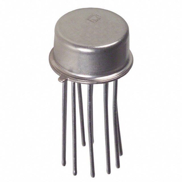
ABSOLUTE MAXIMUM RATINGS ELECTROSTATIC Supply Voltage...................................................................................– 22V DISCHARGE SENSITIVITY Output Sink Current (F )................................................................50mA OUT OInuptuptu Vt oCltuargreen, t– (IVnpOUuTt)...........................................................................................................................................–+S2u0pmplAy This integrated circuit can be damaged by ESD. Burr-Brown Input Voltage, +Input.....................................................................– Supply recommends that all integrated circuits be handled with Comparator Input..........................................................................– Supply appropriate precautions. Failure to observe proper handling and Storage Temperature Range: installation procedures can cause damage. VFC32BM, SM.............................................................–65(cid:176)C to +150(cid:176)C VFC32KP, KU................................................................–25(cid:176)C to +85(cid:176)C ESD damage can range from subtle performance degradation to complete device failure. Precision integrated circuits may be more susceptible to damage because very small parametric PACKAGE/ORDERING INFORMATION changes could cause the device not to meet its published specifi- cations. PACKAGE DRAWING TEMPERATURE PRODUCT PACKAGE NUMBER(1) RANGE VFC32KP 14-Pin Plastic DIP 010 0(cid:176)C to 70(cid:176)C VFC32BM TO-100 Metal 007 –25(cid:176)C to +85(cid:176)C VFC32SM TO-100 Metal 007 –55(cid:176)C to +125(cid:176)C VFC32KU SO-14 SOIC 235 0(cid:176)C to +70(cid:176)C NOTE: (1) For detailed drawing and dimension table, please see end of data sheet, or Appendix C of Burr-Brown IC Data Book. PIN CONFIGURATIONS Top View M Package P Package (TO-100) U Package V (Epoxy Dual-in-line) OUT +In 1 10 –In 1 14 +In Input Amp Input –In 2 9 +VCC NC 2 Amp 13 V OUT NC 3 12 +V One- CC –V (Case) 3 Switch shot 8 Common CC –V 4 11 Common CC h c One-Shot 5 wit 10 Comparator One-Shot 4 7 Comparator Capacitor S Input Capacitor Input NC 6 One- 9 NC 5 6 shot NC fOUT fOUT 7 8 NC NC = no internal connection External connection permitted. The information provided herein is believed to be reliable; however, BURR-BROWN assumes no responsibility for inaccuracies or omissions. BURR-BROWN assumes no responsibility for the use of this information, and all use of such information shall be entirely at the user’s own risk. Prices and specifications are subject to change without notice. No patent rights or licenses to any of the circuits described herein are implied or granted to any third party. BURR-BROWN does not authorize or warrant any BURR-BROWN product for use in life support devices and/or systems. 3 VFC32
TYPICAL PERFORMANCE CURVES At T = +25(cid:176)C and V = – 15V, unless otherwise noted. A CC LINEARITY ERROR vs FULL SCALE FREQUENCY LINEARITY ERROR vs OPERATING FREQUENCY 0.10 1 f = 10kHz, 25% Duty Cycle R) Duty Cycle = 25% FULL SCALE FS at Full Scale TA = +25°C % of Hz) 0.5 Error ( 0.01 Error ( 0 cal Linearity TA = +25°C Linearity –0.5 pi y T 0.001 –1.0 1k 10k 100k 1M 0 1k 2k 3k 4k 5k 6k 7k 8k 9k 10k Full Scale Frequency (Hz) Operating Frequency (Hz) FULL SCALE DRIFT vs FULL SCALE FREQUENCY 1000 C) R/° S F of m p p Drift ( 100 (SM, KP, KU) p m e T (BM) e al c S ull F 10 1k 10k 100k 1M Full Scale Frequency (Hz) VFC32 4
APPLICATION INFORMATION approximately 2.5Vp-p integrator voltage waveform. If C’s 2 value is made too low, the integrator output voltage can Figure 1 shows the basic connection diagram for frequency- exceed its linear output swing, resulting in a nonlinear to-voltage conversion. R sets the input voltage range. For a response. Using C values larger than shown in Figure2 is 10V full-scale input, a 401kW input resistor is recommended. acceptable. 2 Other input voltage ranges can be achieved by changing the Accuracy or temperature stability of C is not critical be- value of R. 2 1 cause its value does not directly affect the output frequency. V R = FS For best linearity, however, C should have low leakage and 1 0.25mA (1) 2 low dielectric absorption. Polycarbonate and other film capacitors are generally excellent. Many ceramic types are R should be a metal film type for good stability. Manufac- 1 adequate, but some low-voltage ceramic capacitor types turing tolerances can produce approximately – 10% variation may degrade nonlinearity. Electrolytic types are not recom- in output frequency. Full-scale output frequency can be mended. trimmed by adjusting the value of R—see Figure 3. 1 The full-scale output frequency is determined by C. Values 1 FREQUENCY OUTPUT PIN shown in Figure 1 are for a full-scale output frequency of The frequency output terminal is an open-collector logic 10kHz. Values for other full-scale frequencies can be read output. A pull-up resistor is usually connected to a 5V logic from Figure 2. Any variation in C—tolerance, temperature 1 supply to create standard logic-level pulses. It can, however, drift, aging—directly affect the output frequency. Ceramic be connected to any power supply up to +V . Output pulses NPO or silver-mica types are a good choice. CC have a constant duration and positive-going during the one- For full-scale frequencies above 200kHz, use larger capaci- shot period. Current flowing in the open-collector output tor values as indicated in Figure 2, with R = 20kW . 1 transistor returns through the Common terminal. This termi- The value of the integrating capacitor, C, does not directly nal should be connected to logic ground. 2 influence the output frequency, but its value must be chosen within certain bounds. Values chosen from Figure 2 produce f O V INT Pull-Up Voltage 0V £ V £ +V +15V PU CC +5V C 0.1µF 2 10nF film V INT R4.P7UkW RVPU £ 8mA PU R 1 40kW fOUT V IN 0 to 10kHz 0 to 10V One-Shot VFC32 0.1µF Pinout shown is C 1 for DIP or SOIC 3.3nF packages. NPO Ceramic –15V FIGURE 1. Voltage-to-Frequency Converter Circuit. 5 VFC32
FREQUENCY-TO-VOLTAGE CONVERSION PRINCIPLES OF OPERATION Figure 4 shows the VFC32 connected as a frequency-to- The VFC32 operates on a principle of charge balance. The voltage converter. The capacitive-coupled input network C, signal input current is equal to V /R. This current is 3 IN 1 R and R allow standard 5V logic levels to trigger the integrated by input op amp and C, producing a downward 6 7 2 comparator input. The comparator triggers the one-shot on ramping integrator output voltage. When the integrator out- the falling edge of the frequency input pulses. Threshold put ramps to the threshold of the comparator, the one-shot is voltage of the comparator is approximately –0.7V. For triggered. The 1mA reference current is switched to the frequency input waveforms less than 5V logic levels, the integrator input during the one-shot period, causing the R/R voltage divider can be adjusted to a lower voltage to integrator output ramp upward. After the one-shot period, 6 7 assure that the comparator is triggered. the integrator again ramps downward. The value of C is chosen from Figure 2 according to the The oscillation process forces a long-term balance of charge 1 full-scale input frequency. C smooths the output voltage (or average current) between the input signal current and the 2 waveform. Larger values of C reduce the ripple in the reference current. The equation for charge balance is: 2 output voltage. Smaller values of C allow the output voltage 2 to settle faster in response to a change in input frequency. I =I (2) IN R(AVERAGE) Resistor R can be trimmed to achieve the desired output 1 voltage at the full-scale input frequency. V IN =f t (1mA) (3) R O OS 1 0.1µF C Where: 2 f is the output frequency 10nF O t is the one-shot period, equal to e OS Valu tOS = 7500 C1 (Farads) (4) or 1nF C = 3 3 , 0 0 0 p F – 30pF apacit 1 R1fF =S (4kH0zk)W The values suggested for R1 and C1 are chosen to produce a C 25% duty cycle at full-scale frequency output. For full-scale 100pF Above 200kHz Full-Scale 66,000pF frequencies above 200kHz, the recommended values pro- C = – 30pF 1 fFS (kHz) duce a 50% duty cycle. R = 20kW 10pF 1 1k 10k 100k 1M Full Scale Frequency (Hz) FIGURE 2. Capacitor Value Selection. +5V C V +15V 2 INT 0.1µF 4.7kW 13 10 12 Gain Trim 7 10kW 35kW 1 fO V IN One-Shot 14 +15V 10MW Offset 11 1mA Trim 100kW VFC32 –15V 4 5 C 1 Pinout shown is for 33nF DIP and SOIC packages. –15V FIGURE 3. Gain and Offset Voltage Trim Circuit. VFC32 6
+15V 2.5V 0V 0V 12kW –2.5V 0 to 10kHz 500pF f IN 5V Logic 2.2kW C2 Input 0.1µF V O 0 to 10V R1 +15V 40kW 13 10 12 7 10MW NC 1 +15V One-Shot 14 100kW –15V 11 VFC32 4 5 C 1 3.3nF –15V FIGURE 4. Frequency-to-Voltage Converter Circuit. +15V +5V C 0.1µF 2 2nF 13 10 12 7 f 1 OUT 0 to 50kHz One-Shot 14 V IN 0V to –10V R 40k1W 11 VFC32 0.1µF 4 5 Nonlinearity may be higher than C1 Pinout shown is specified due to common-mode 650pF for DIP or SOIC voltage on op amp input. package. –15V FIGURE 5. V/F Converter—Negative Input Voltage. 7 VFC32
PACKAGE OPTION ADDENDUM www.ti.com 6-Feb-2020 PACKAGING INFORMATION Orderable Device Status Package Type Package Pins Package Eco Plan Lead/Ball Finish MSL Peak Temp Op Temp (°C) Device Marking Samples (1) Drawing Qty (2) (6) (3) (4/5) VFC32KP ACTIVE PDIP N 14 25 Green (RoHS NIPDAU N / A for Pkg Type 0 to 70 VFC32KP & no Sb/Br) VFC32KPG4 ACTIVE PDIP N 14 25 Green (RoHS NIPDAU N / A for Pkg Type 0 to 70 VFC32KP & no Sb/Br) VFC32KU ACTIVE SOIC D 14 50 Green (RoHS NIPDAU Level-3-260C-168 HR 0 to 70 VFC32KU & no Sb/Br) VFC32KU/2K5 ACTIVE SOIC D 14 2500 Green (RoHS NIPDAU Level-3-260C-168 HR 0 to 70 VFC32KU & no Sb/Br) VFC32KUE4 ACTIVE SOIC D 14 50 Green (RoHS NIPDAU Level-3-260C-168 HR 0 to 70 VFC32KU & no Sb/Br) (1) The marketing status values are defined as follows: ACTIVE: Product device recommended for new designs. LIFEBUY: TI has announced that the device will be discontinued, and a lifetime-buy period is in effect. NRND: Not recommended for new designs. Device is in production to support existing customers, but TI does not recommend using this part in a new design. PREVIEW: Device has been announced but is not in production. Samples may or may not be available. OBSOLETE: TI has discontinued the production of the device. (2) RoHS: TI defines "RoHS" to mean semiconductor products that are compliant with the current EU RoHS requirements for all 10 RoHS substances, including the requirement that RoHS substance do not exceed 0.1% by weight in homogeneous materials. Where designed to be soldered at high temperatures, "RoHS" products are suitable for use in specified lead-free processes. TI may reference these types of products as "Pb-Free". RoHS Exempt: TI defines "RoHS Exempt" to mean products that contain lead but are compliant with EU RoHS pursuant to a specific EU RoHS exemption. Green: TI defines "Green" to mean the content of Chlorine (Cl) and Bromine (Br) based flame retardants meet JS709B low halogen requirements of <=1000ppm threshold. Antimony trioxide based flame retardants must also meet the <=1000ppm threshold requirement. (3) MSL, Peak Temp. - The Moisture Sensitivity Level rating according to the JEDEC industry standard classifications, and peak solder temperature. (4) There may be additional marking, which relates to the logo, the lot trace code information, or the environmental category on the device. (5) Multiple Device Markings will be inside parentheses. Only one Device Marking contained in parentheses and separated by a "~" will appear on a device. If a line is indented then it is a continuation of the previous line and the two combined represent the entire Device Marking for that device. (6) Lead/Ball Finish - Orderable Devices may have multiple material finish options. Finish options are separated by a vertical ruled line. Lead/Ball Finish values may wrap to two lines if the finish value exceeds the maximum column width. Addendum-Page 1
PACKAGE OPTION ADDENDUM www.ti.com 6-Feb-2020 Important Information and Disclaimer:The information provided on this page represents TI's knowledge and belief as of the date that it is provided. TI bases its knowledge and belief on information provided by third parties, and makes no representation or warranty as to the accuracy of such information. Efforts are underway to better integrate information from third parties. TI has taken and continues to take reasonable steps to provide representative and accurate information but may not have conducted destructive testing or chemical analysis on incoming materials and chemicals. TI and TI suppliers consider certain information to be proprietary, and thus CAS numbers and other limited information may not be available for release. In no event shall TI's liability arising out of such information exceed the total purchase price of the TI part(s) at issue in this document sold by TI to Customer on an annual basis. Addendum-Page 2
PACKAGE MATERIALS INFORMATION www.ti.com 14-Jul-2012 TAPE AND REEL INFORMATION *Alldimensionsarenominal Device Package Package Pins SPQ Reel Reel A0 B0 K0 P1 W Pin1 Type Drawing Diameter Width (mm) (mm) (mm) (mm) (mm) Quadrant (mm) W1(mm) VFC32KU/2K5 SOIC D 14 2500 330.0 16.4 6.5 9.0 2.1 8.0 16.0 Q1 PackMaterials-Page1
PACKAGE MATERIALS INFORMATION www.ti.com 14-Jul-2012 *Alldimensionsarenominal Device PackageType PackageDrawing Pins SPQ Length(mm) Width(mm) Height(mm) VFC32KU/2K5 SOIC D 14 2500 367.0 367.0 38.0 PackMaterials-Page2
IMPORTANTNOTICEANDDISCLAIMER TI PROVIDES TECHNICAL AND RELIABILITY DATA (INCLUDING DATASHEETS), DESIGN RESOURCES (INCLUDING REFERENCE DESIGNS), APPLICATION OR OTHER DESIGN ADVICE, WEB TOOLS, SAFETY INFORMATION, AND OTHER RESOURCES “AS IS” AND WITH ALL FAULTS, AND DISCLAIMS ALL WARRANTIES, EXPRESS AND IMPLIED, INCLUDING WITHOUT LIMITATION ANY IMPLIED WARRANTIES OF MERCHANTABILITY, FITNESS FOR A PARTICULAR PURPOSE OR NON-INFRINGEMENT OF THIRD PARTY INTELLECTUAL PROPERTY RIGHTS. These resources are intended for skilled developers designing with TI products. You are solely responsible for (1) selecting the appropriate TI products for your application, (2) designing, validating and testing your application, and (3) ensuring your application meets applicable standards, and any other safety, security, or other requirements. These resources are subject to change without notice. TI grants you permission to use these resources only for development of an application that uses the TI products described in the resource. Other reproduction and display of these resources is prohibited. No license is granted to any other TI intellectual property right or to any third party intellectual property right. TI disclaims responsibility for, and you will fully indemnify TI and its representatives against, any claims, damages, costs, losses, and liabilities arising out of your use of these resources. TI’s products are provided subject to TI’s Terms of Sale (www.ti.com/legal/termsofsale.html) or other applicable terms available either on ti.com or provided in conjunction with such TI products. TI’s provision of these resources does not expand or otherwise alter TI’s applicable warranties or warranty disclaimers for TI products. Mailing Address: Texas Instruments, Post Office Box 655303, Dallas, Texas 75265 Copyright © 2020, Texas Instruments Incorporated