ICGOO在线商城 > 电路保护 > TVS - 变阻器,MOV > V5.5MLA0603LNR
 Datasheet下载
- 型号: V5.5MLA0603LNR
- 制造商: Littelfuse
- 库位|库存: xxxx|xxxx
- 要求:
| 数量阶梯 | 香港交货 | 国内含税 |
| +xxxx | $xxxx | ¥xxxx |
查看当月历史价格
查看今年历史价格
V5.5MLA0603LNR产品简介:
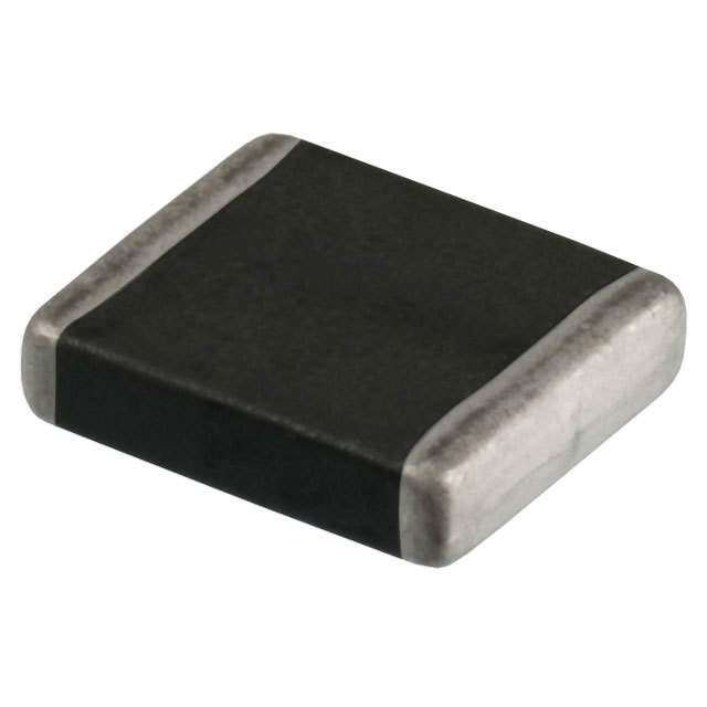
ICGOO电子元器件商城为您提供V5.5MLA0603LNR由Littelfuse设计生产,在icgoo商城现货销售,并且可以通过原厂、代理商等渠道进行代购。 V5.5MLA0603LNR价格参考。LittelfuseV5.5MLA0603LNR封装/规格:TVS - 变阻器,MOV, 8.2V 30A Varistor 1 Circuit 表面贴装,MLCV 0603(1608 公制)。您可以下载V5.5MLA0603LNR参考资料、Datasheet数据手册功能说明书,资料中有V5.5MLA0603LNR 详细功能的应用电路图电压和使用方法及教程。
Littelfuse Inc. 的型号为 V5.5MLA0603LNR 的产品是一款多层压敏电阻(MLV),属于TVS(瞬态电压抑制)中的MOV(金属氧化物压敏电阻)类别,封装尺寸为0603,额定电压为5.5V。该器件主要用于保护敏感电子元件免受静电放电(ESD)、电压突波和瞬态过压事件的损害。

其典型应用场景包括:

1. 便携式消费类电子产品:广泛应用于智能手机、平板电脑、可穿戴设备(如智能手表)等,用于保护数据接口(如USB、HDMI)和电源线路免受ESD冲击。

2. 通信接口保护:适用于I²C、SPI、UART等低电压信号线路,提供快速响应的过压保护,确保信号完整性。

3. 电池供电设备:在蓝牙耳机、无线传感器、小型IoT设备中,用于防止因静电或意外接触高压引发的损坏。

4. 汽车电子模块:用于车载信息娱乐系统、传感器接口等低压电路中,满足车规级可靠性要求。

5. 工业控制与便携仪器:保护精密模拟前端和数字控制线路,提升系统稳定性。

V5.5MLA0603LNR 具有小尺寸、低电容(有利于高速信号传输)、高重复性ESD耐受能力(可达±30kV接触放电)等优点,特别适合空间受限且需高可靠性的应用。其无铅环保设计也符合RoHS标准,适用于现代绿色电子产品制造。
| 参数 | 数值 |
| 产品目录 | |
| 描述 | VARISTOR 7.1V 30A 0603压敏电阻 MULTI-LAYER VARISTOR SURFACE MOUNT |
| 产品分类 | |
| 品牌 | Littelfuse |
| 产品手册 | |
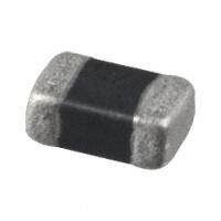
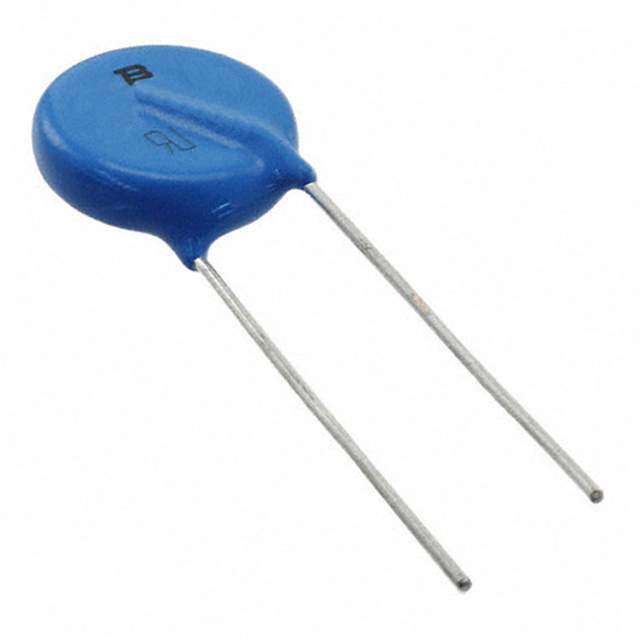
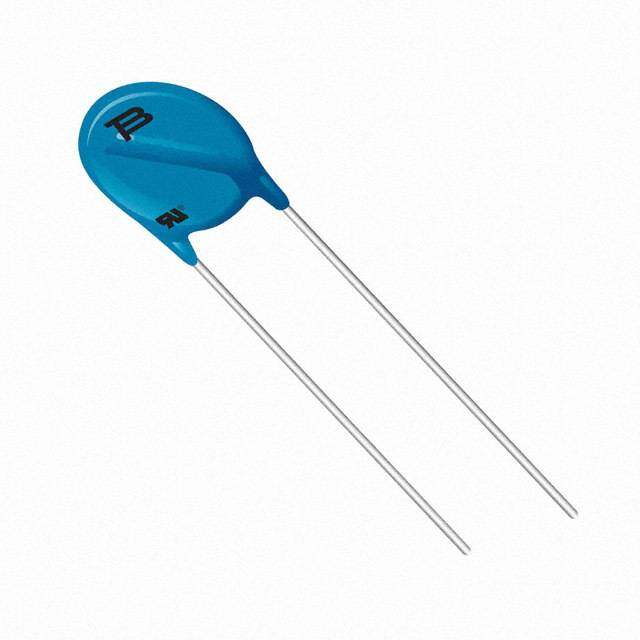
| 产品图片 |
|
| rohs | 符合RoHS无铅 / 符合限制有害物质指令(RoHS)规范要求 |
| 产品系列 | Littelfuse V5.5MLA0603LNRMLA |
| 数据手册 | |
| 产品型号 | V5.5MLA0603LNR |
| 产品 | MLV |
| 产品种类 | 压敏电阻 |
| 其它名称 | F5713DKR |
| 包装 | Digi-Reel® |
| 变阻器电压 | 7.1V |
| 商标 | Littelfuse |
| 外壳代码-in | 0603 |
| 外壳代码-mm | 1608 |
| 外壳宽度 | 0.8 mm |
| 安装 | SMD/SMT |
| 宽度 | 0.8 mm |
| 封装 | Reel |
| 封装/外壳 | 0603(1608 公制) |
| 封装/箱体 | 0603 (1608 metric) |
| 尺寸 | 0.8 mm W |
| 峰值浪涌电流 | 30 A |
| 工作温度范围 | - 55 C to + 125 C |
| 工厂包装数量 | 4000 |
| 最大AC电压 | 4VAC |
| 最大DC电压 | 5.5VDC |
| 标准包装 | 1 |
| 浪涌能量额定值 | 0.1 J |
| 电压 | 7.1 V to 9.3 V |
| 电压额定值AC | 4 V |
| 电压额定值DC | 5.5 V |
| 电容 | 450 pF |
| 电流-浪涌 | 30A |
| 电路数 | 1 |
| 端接类型 | SMD/SMT |
| 系列 | MLA |
| 能量 | 0.10J |
| 钳位电压 | 17.5 V |


- 商务部:美国ITC正式对集成电路等产品启动337调查
- 曝三星4nm工艺存在良率问题 高通将骁龙8 Gen1或转产台积电
- 太阳诱电将投资9.5亿元在常州建新厂生产MLCC 预计2023年完工
- 英特尔发布欧洲新工厂建设计划 深化IDM 2.0 战略
- 台积电先进制程称霸业界 有大客户加持明年业绩稳了
- 达到5530亿美元!SIA预计今年全球半导体销售额将创下新高
- 英特尔拟将自动驾驶子公司Mobileye上市 估值或超500亿美元
- 三星加码芯片和SET,合并消费电子和移动部门,撤换高东真等 CEO
- 三星电子宣布重大人事变动 还合并消费电子和移动部门
- 海关总署:前11个月进口集成电路产品价值2.52万亿元 增长14.8%


PDF Datasheet 数据手册内容提取
Metal-Oxide Varistors (MOVs) Surface Mount Multilayer Varistors (MLVs) > MLA Automotive Series MLA Automotive Varistor Series RoHS Description The MLA Automotive Series of transient voltage surge suppression devices is based on the Littelfuse Multilayer fabrication technology. These components are designed to suppress a variety of transient events, including those specified in IEC 61000-4-2 or other standards used for Electromagnetic Compliance (EMC). The MLA Automotive Series is typically applied to protect integrated circuits and other components at the circuit board level. The wide operating voltage and energy range make the MLA Automotive Series suitable for numerous applications on power supply, control and signal lines. The MLA Automotive Series is manufactured from Size Table semiconducting ceramics, and is supplied in a leadless, surface mount package. The MLA Automtove Series Metric EIA is compatible with modern reflow and wave soldering 1608 0603 procedures. 2012 0805 It can operate over a wider temperature range than Zener 3216 1206 diodes, and has a much smaller footprint than plastic- 3225 1210 housed components. Features Absolute Maximum Ratings • AEC-Q200 qualified • Rated for energy • For ratings of individual members of a series, see device ratings and specifications table. MLA Auto • Halogen-Free and (10 x 1000µs) Continuous Units Series RoHS compliant • Inherent bi-directional Steady State Applied Voltage: • Leadless 0603, 0805, clamping DC Voltage Range (VM(DC)) 3.5 to 120 V 1206 and 1210 chip sizes • No plastic or epoxy AC Voltage Range (VM(AC)RMS) 2.5 to 107 V • Multilayer ceramic packaging assures Transient: construction technology better than UL94V-0 flammability rating Non-Repetitive Surge Current, 8/20µs • -40°C to +125°C up to 500 A Waveform, (ITM) operating temp. range • Standard low capacitance types Non-Repetitive Surge Energy, 10/1000µs • Operating voltage range 0.1 to 2.5 J available Waveform, (WTM) V = 3.5V to 120V M(DC) • Load Dump energy • Rated for surge Operating Ambient Temperature Range (T) -40 to +125 ºC rated per SAE A current (8 x 20µs) Specification J1113 Storage Temperature Range (T ) -40 to +150 ºC STG Applications Temperature Coefficient (αV) of Clamping Voltage <0.01 %/º C • Suppression of • Provides on-board (V) at Specified Test Current C inductive switching transient voltage or other transient protection for ICS events such as EFT and transistors and surge voltage at • Used to help achieve Additional Information the circuit board level electromagnetic • ESD protection for IEC compliance of 61000-4-2, MIL-STD- end products 883c method 3015.7, • Replaces larger surface and other industry mount TVS Zeners in Datasheet Resources Samples specifications many applications © 2020 Littelfuse, Inc. Specifications are subject to change without notice. Revised: 02/21/20
Metal-Oxide Varistors (MOVs) Surface Mount Multilayer Varistors (MLVs) > MLA Automotive Series Device Ratings and Specifications Maximum Ratings (125º C) Specifications (25ºC) Maximum Jump Maximum Maximum Load Maximum Non- Clamping Nominal Voltage Typical Start Non-repetitive Continuous Dump repetitive Surge Voltage at 1A at 1mA DC Test Capacitance at Voltage Surge Energy Part Number Working Voltage Energy Current (8/20µs) (or as Noted) Current f = 1MHz (5 min) (10/1000µs) (8/20µs) V V V V W I W V V Min N(DC) C M(DC) M(AC) JUMP LD TM TM C N(DC) Max (V) (V) (V) (J) (A) (J) (V) (V) (V) (pF) V3.5MLA0603NHAUTO 3.5 2.5 -- -- 30 0.100 13.0 3.7 7.0 860 V3.5MLA0805NHAUTO 3.5 2.5 -- -- 120 0.300 13.0 3.7 7.0 1500 V3.5MLA0805LNHAUTO 3.5 2.5 -- -- 40 0.100 13.0 3.7 7.0 1080 V3.5MLA1206NHAUTO 3.5 2.5 -- -- 100 0.300 13.0 3.7 7.0 3000 V5.5MLA0603NHAUTO 5.5 4.0 -- -- 30 0.100 17.5 7.1 9.3 830 V5.5MLA0805NHAUTO 5.5 4.0 -- -- 120 0.300 17.5 7.1 9.3 1200 V5.5MLA0805LNHAUTO 5.5 4.0 -- -- 40 0.100 17.5 7.1 9.3 400 V5.5MLA1206NHAUTO 5.5 4.0 -- -- 150 0.400 17.5 7.1 9.3 2900 V9MLA0603NHAUTO 9.0 6.5 -- -- 30 0.100 25.5 11.0 16.0 210 V9MLA0805LNHAUTO 9.0 6.5 -- -- 40 0.100 25.5 11.0 16.0 400 V12MLA0805LNHAUTO 12.0 9.0 -- -- 40 0.100 29.0 14.0 18.5 210 V14MLA0603NHAUTO 14.0 10.0 -- -- 30 0.100 34.5 15.9 21.5 90 V14MLA0805NHAUTO 14.0 10.0 -- -- 120 0.300 32.0 15.9 20.3 560 V14MLA0805LNHAUTO 14.0 10.0 -- -- 40 0.100 32.0 15.9 20.3 320 V14MLA1206NHAUTO 14.0 10.0 -- -- 150 0.400 32.0 15.9 20.3 800 V18MLA0603NHAUTO 18.0 14.0 24.5 0.3 30 0.100 50.0 22.0 28.0 120 V18MLA0805NHAUTO 18.0 14.0 24.5 1 120 0.300 44.0 22.0 28.0 245 V18MLA0805LNHAUTO 18.0 14.0 24.5 0.7 40 0.100 44.0 22.0 28.0 180 V18MLA1206NHAUTO 18.0 14.0 24.5 1.5 150 0.400 44.0 22.0 28.0 1050 V18MLA1210NHAUTO 18.0 14.0 24.5 3 500 2.500 44.0 at 2.5 22.0 28.0 2500 V26MLA0603NHAUTO 26.0 20.0 27.5 0.4 30 0.100 60.0 31.0 38.0 50 V26MLA0805NHAUTO 26.0 20.0 27.5 1 100 0.300 60.0 29.5 38.5 110 V26MLA0805LNHAUTO 26.0 20.0 27.5 0.7 40 0.100 60.0 29.5 38.5 90 V26MLA1206NHAUTO 26.0 20.0 27.5 1.5 150 0.600 60.0 29.5 38.5 600 V26MLA1210NHAUTO 26.0 20.0 27.5 3 300 1.200 60.0 at 2.5 29.5 38.5 1260 V30MLA0603NHAUTO 30.0 25.0 29 0.4 30 0.100 74.0 37.0 46.0 45 V30MLA0805LNHAUTO 30.0 25.0 29 0.7 30 0.100 72.0 37.0 46.0 80 V30MLA0805NHAUTO 30.0 25.0 29 1 80 0.300 72.0 37.0 46.0 100 V30MLA1210NHAUTO 30.0 25.0 29 3 280 1.200 68.0 at 2.5 35.0 43.0 690 V30MLA1210LNHAUTO 30.0 25.0 29 3 220 0.900 68.0 at 2.5 35.0 43.0 500 V33MLA1206NHAUTO 33.0 26.0 36 1.5 180 0.800 75.0 38.0 49.0 380 V42MLA1206NHAUTO 42.0 30.0 48 1.5 180 0.800 92.0 46.0 60.0 340 V48MLA1210NHAUTO 48.0 40.0 48 3 250 1.200 105.0 at 2.5 54.5 66.5 400 V48MLA1210LNHAUTO 48.0 40.0 - - 220 0.90 105.0 at 2.5 54.5 66.5 320 V48MLA1206NHAUTO 48.0 40.0 48 1.5 180 0.90 100 54.5 66.5 180 V56MLA1206NHAUTO 56.0 40.0 48 1.5 180 1.00 120.0 61.0 77.0 150 V60MLA1210NHAUTO 60.0 50.0 48 3 250 1.50 130.0 at 2.5 67.0 83.0 230 V68MLA1206NHAUTO 68.0 50.0 48 1.5 180 1.00 140.0 76.0 90.0 130 V85MLA1210NHAUTO 85.0 67.0 48 3 150 2.50 180.0 at 2.5 95.0 115.0 160 V120MLA1210NHAUTO 120.0 107.0 48 3 125 2.00 260.0 at 2.5 135.0 165.0 80 NOTES: 1. 'L' suffix is a low capacitance and energy version; Contact your Littelfuse sales representative for custom capacitance requirements 2. Typical leakage at 25ºC<25µA, maximum leakage 100µA at V M(DC) 3. Average power dissipation of transients for 0603, 0805, 1206 and 1210 sizes not to exceed 0.05W, 0.1W, 0.1W and 0.15W respectively 4. Load dump :min. time of energy input 40ms, interval 60sec(the load dump time constant Td differs from the time constant of energy input; load dump rating for ISO 7637-2 pulse 5a and ISO16750-2 Table 5A. Please contact Littelfuse. © 2020 Littelfuse, Inc. Specifications are subject to change without notice. Revised: 02/21/20
Metal-Oxide Varistors (MOVs) Surface Mount Multilayer Varistors (MLVs) > MLA Automotive Series Peak Current and Energy Derating Curve Peak Pulse Current Test Waveform for Clamping Voltage When transients occur in rapid succession, the average power dissipation is the energy (watt-seconds) per pulse E 100 U times the number of pulses per second. The power so L A V developed must be within the specifications shown K A on the Device Ratings and Specifications Table for the E specific device. For applications exceeding 125°C ambient OF P 50 temperature, the peak surge current and energy ratings NT E must be derated as shown below. RC PE 0 T UE 100 O1 TIME AL T1 V ED 80 Figure 2 T2 T RA 60 OF 0 = Virtual Origin of Wave NT 40 T1 = Time from 10% to 90% of Peak CE 20 T =F IRGiUsReE T i2m. eP E=A K1 .P2U5L xS ET CURRENT TEST WAVEFORM R 1 FOR CLAMPING VOLTAGE PE 0 T2 = Decay Time -55 50 60 70 80 90 100 110 120 130 140 150 Example - For an 8/20 µs Current Waveform: AMBIENT TEMPERATURE (oC) O18t =µ= TsVII MR=TE TU F1AR L=O O MRR iI1sG0eI%N T TOiOmF 9We0A%V EOF PEAK t21 0= µVIsR T=U TAL =FR DONeTc aTIyM TEi m= 1e.25 x t Figure 1 t2 = VIRTUA2L TIME TO HALF VALUE (IMPULSE DURATION) EXAMPLE: FOR AN 8/20 s CURRENT WAVEFORM 8 s = t1 = VIRTUAL FRONT TIME 20 s = t2 = VIRTUAL TIME TO HALF VALUE © 2020 Littelfuse, Inc. Specifications are subject to change without notice. Revised: 02/21/20
Metal-Oxide Varistors (MOVs) Surface Mount Multilayer Varistors (MLVs) > MLA Automotive Series Limit V-I Characteristic for V3.5MLA0603NHAUTO to Limit V-I Characteristic for V3.5MLA0805LNHAUTO to V30MLA0603NHAUTO V30MLA0805LNHAUTO 1000 1000 V30MLA0805LNHAUTO V30MLA0603NHAUTO V26MLA0805LNHAUTO V26MLA0603NHAUTO V18MLA0805LNHAUTO 100 VV1184MMLLAA00660033NNHHAAUUTTOO 100 V14MLA0805LNHAUTO Varistor Voltage (V)10 VVVV5599..MM55MMLLAALLAA00660000663300NL33NNLHNHHAHAUAUAUTUOTTOOT, O, Varistor Voltage (V) 10 VV192MMLALA00880055LNLNHHAAUUTOTO V3.5MLA0603NHAUTO V5.5MLA0805LNHAUTO V3.5MLA0805LNHAUTO 1 1 10µA 100µA 1mA 10mA 100mA 1A 10A 100A 10µA 100µA 1mA 10mA 100mA 1A 10A 100A Figure 3 Current (A) Figure 4 Current (A) Limit V-I CharaFIGcUtReE Xr. iLsIMtITi Vc-I CfHoARrAC VTER3IST.I5C FMOR VL3.5AML0A086003N5HANUTOH TOA V3U0MTLAO060 3tNoHA UTO LimFIGiUtR VE X-.I L ICMIhT Va-Ir CaHAcRtAeCrTEiRsIStTiIcC FfOoR rV3 V.5M3L.A508M05LLNAHA1U2TO0 T6O VN30HMLAA0U80T5LONH AtUoTO V26MLA0805NHAUTO V42MLA1206NHAUTO 1000 1000 V30MLA0805LNHAUTO V26MLA0805LNHAUTO V18MLA0805LNHAUTO 100 V14MLA0805LNHAUTO Varistor Voltage (V) 10 VVV519.2M5MMLALLA0A0808080505L5NLLNHNHAHAUAUTUOTTOO Varistor Voltage (V)11000 VVVVV113VVVVVV2448362432115MMMMM23684.5LLLLLMMMMMAAAAAM1V1111LLLLL22222L5VAAAAA000006VA466666M11111681NNNNN8L22222M2HHHHHMA00000LA0AAAA1LA66666UUUUU2A610TTTTT126OOOOO20N06H6NNAHHUAATUOUTTOO 1 V3.5MLA0805LNHAUTO VV53V..553MM.5LLMAA11L220A0661NN2HH0AA6UUTTOO 10µA 100µA 1mA 10mA 100mA 1A 10A 100A Current (A) Figure 5 1 10µA 100µA 1mA 10mA 100mA 1A 10A 100A 1000A Current (A) FIGURE X. LIMIT V-I CHARACTERISTIC FOR V3.5MLA0805LNHAUTO TO V30MLA0805LNHAUTO Figure 7 Limit V-I Characteristic for V18MLA1210NHAUTO to FIGURE 6. LIMIT V-1 CHARACTERISTIC FOR V3.5MLA1206 TO V68MLA1206 V48MLA1210NHAUTO 1000 100 Varistor Voltage (V) VV3408MMLLAA11221100NNHHAAUUTTOO,, VV3408MMV6LL0AAM1122L11VA0081LL52NNM1HH0LAANAUUH1TTVA2OO1U120T0NOMHLAAU1T2O10NHAUTO 10 V26MLA1210NHAUTO V18MLA1210NHAUTO 1 10µA 100µA 1mA 10mA 100mA 1A 10A 100A 1000A CURRENT (A) Figure 6 FIGURE X. LIMIT V-I CHARACTERISTIC FOR V18MLA1210NHAUTO TO V120MLA1210NHAUTO © 2020 Littelfuse, Inc. Specifications are subject to change without notice. Revised: 02/21/20
Metal-Oxide Varistors (MOVs) Surface Mount Multilayer Varistors (MLVs) > MLA Automotive Series Device Characteristics Clamping Voltage Over Temperature (V at 10A) C At low current levels, the V-I curve of the multilayer transient voltage suppressor approaches a linear (ohmic) 100 relationship and shows a temperature dependent effect. Aist ino ra b heilgohw r ethseis tmanacxeim mumod ewxo (rakpinpgro vaoclhtaingge ,1 t0h6eΩ s autp iptsr essor GE (V) V26MLA1206 A maximum rated working voltage). Leakage currents at LT O maximum rated voltage are below 100µA, typically 25µA. G V N PI M Typical Temperature Dependance of the Haracteristic A L C Curve in the Leakage Region V5.5MLA1206 100% OF GE IN PERCENT oAT 25C (%) FigureF1 I0G9-6U0RE- 4102. C-L2A0MPI0NGT EVM2O0PLETRAAG4T0EU ROE6V (0EoCR) T8E0MP1E0R0ATU12R0E140 ESSOR VOLTA VALUE VNOM Energy Absorp(VtiCo AnT/ P10eAa)k Current Capability R PP Energy dissipated within the MLA Automotive Series is SU 25o 50o 75o 100o 125oC 10% calculated by multiplying the clamping voltage, transient 1E-9 1E-8 1E-7 1E-6 1E-5 1E-4 1E-3 1E-2 current and transient duration. An important advantage of Figure 8 SUPPRESSOR CURRENT (ADC) FIGURE 10. TYPICAL TEMPERATURE DEPENDANCE OF THE CHARACTERISTIC the multilayer is its interdigitated electrode construction CURVE IN THE LEAKAGE REGION within the mass of dielectric material. This results in excellent current distribution and the peak temperature per energy absorbed is very low. The matrix of semiconducting Speed of Response grains combine to absorb and distribute transient energy (heat) (see Speed of Response). This dramatically reduces The Multilayer Suppressor is a leadless device. Its peak temperature; thermal stresses and enhances device response time is not limited by the parasitic lead reliability. inductances found in other surface mount packages. The response time of the Z O dielectric material is less than As a measure of the device capability in energy and peak N 1ns and the MLA Automotive Series can clamp very fast current handling, the V26MLA1206 part was tested with dV/dT events such as ESD. Additionally, in "real world" multiple pulses at its peak current rating (150A, 8/20µs). At applications, the associated circuit wiring is often the the end of the test,10,000 pulses later, the device voltage greatest factor effecting speed of response. Therefore, characteristics are still well within specification. transient suppressor placement within a circuit can be considered important in certain instances. Repetitive Pulse Capability Multilayer Internal Construction FIREDDI ECLEERCATMRIICC 100 PEAK CURRENT = 3A 8/20s DURATION, 30s BETWEEN PULSES E V26MLA1206 G A METAL OLT ELECTRODES V METAL END TERMINATION DEPLETION REGION 10 0 2000 4000 6000 8000 10000 12000 DEPRLEEGTIIOONN Figure 11 NUMBER OF PULSES Figure 10 FIGURE 13. REPETITIVE PULSE CAPABILITY GRAINS FIGURE 11. MULTILAYER INTERNAL CONSTRUCTION © 2020 Littelfuse, Inc. Specifications are subject to change without notice. Revised: 02/21/20
Metal-Oxide Varistors (MOVs) Surface Mount Multilayer Varistors (MLVs) > MLA Automotive Series Lead (Pb) Soldering Recommendations The principal techniques used for the soldering of Reflow Solder Profile components in surface mount technology are IR Re-flow and Wave soldering. Typical profiles are shown on the right. 250 250 MAXIMUM TEMPERATURE The recommended solder for the MLA Automotive Series MAXIMUM 2T3E0M°CPERATURE 220500 230°C s(WSunapv/pPerb es)s.o sLldoitert erisilnf aug s 6ies2 t/a3hls6eo/ 2m r e(oScsnot/ mPstbmr/eAengnu)do, su6 sa0 n/o4 fR0 t Mh(SeAn p/sProoblc)d eoesrr s6fle3us/x.3 .7 URE °CATURE °CC221105050000 MAXIMUM 2T3ER0M°ACPMEPR ARAATABBSSSUTOEOEERE444CCVCVE000EOEOO---888 NNN1100088DDD33SSS°°CC To avoid the possibility of generating stresses due to RATPERRE ° 110500 R<<22A°°MCCP//ss RAABTOEVE 183°C thermal shock, a preheat stage in the soldering process EMPETEMRATU100 PPRREEHHEEAATT DDWWEELLR<LL2A°MCP/s RATE is recommended, and the peak temperature of the solder TPE 10500 PREHEAT ZONE process should be rigidly controlled. EM 50 PREHPERAETH EZOATN EDWELL T 500 PREHEAT ZONE When using a reflow process, care should be taken 00 0.5 1.0 1.5 2.0 2.5 3.0 3.5 4.0 to ensure that the MLA Automotive Series chip is not 0 0.5 1.0 1.T5I M E ( M2I.N0 U T E S2).5 3.0 3.5 4.0 Figure 120 TIME (MINUTES) subjected to a thermal gradient steeper than 4 degrees 0 F 0IG.5U R E 1 1.04 . R E 1F.5L O W S2.O0 L D E 2R.5 P R O F3.I0L E 3.5 4.0 per second; the ideal gradient being 2 degrees per second. FIGURE 14. REFTLIMOEW ( MSIONLUDTEESR) PROFILE Wave Solder Profile During the soldering process, preheating to within 100 FIGURE 14. REFLOW SOLDER PROFILE degrees of the solder's peak temperature is essential to minimize thermal shock. 300 300 MAXIMUM WAVE 260°C Once the soldering process has been completed, it is 235000 MAXIMUM WAVE 260°C 250 still necessary to ensure that any further thermal shocks are avoided. One possible cause of thermal shock is hot CE °C 220500 MAXIMUM WAVE 260°C pprrioncteesds c airncdu ist ubbojaercdtse db etoin cgl ereamninogv esdo lfvreonmts t haet rsoooldme r ATURE °ERATURE °C 211255000000 SECOND PREHEAT RPR tteom lepsesr athtuarne 5. T0hº eC bboeafrodrse mcleuasnt ibneg .allowed to cool gradually TEMPETEMPERATU 111005000 FIRST PREHEASSTEECCOONNDD PPRREEHHEEAATT M 50 FIRST PREHEAT E 100 T 50 FIRST PREHEAT 0 5000.0 0.5 1.0 1.5 2.0 2.5 3.0 3.5 4.0 4.5 Figure 130.0 0.5 1.0 1.5TIM2E. 0(MINU2.T5ES)3.0 3.5 4.0 4.5 0 TIME (MINUTES) 0.0 0F.5IGUR1.0E 15.1.W5AVE2 .S0OLD2.E5R PR3.O0FIL3E.5 4.0 4.5 Lead–free (Pb-free) Soldering Recommendations FIGURE 15. WATIVMEE S(MOILNDUTEERS P)ROFILE FIGURE 15. WAVE SOLDER PROFILE Littelfuse offers the Nickel Barrier Termination option (see Lead–free Re-flow Solder Profile "N" suffix in Part Numbering System for ordering) for the 300 optimum Lead–free solder performance, consisting of a 300 MAXIMUM TEMPERATURE 260˚C, MTIAMXEI MWUITMH TINE M5˚PCE ORFA TPUERAEK 260˚C, Matte Tin outer surface plated on Nickel underlayer, plated 320500 T20IM SEE WCOITNHDINS 5M˚CA XOIFM UPEMAK oTflhnue xS, piblvrueetfr e tbrhraeesrdee smiso leadt eawrl .ii dse 9 s6e.5le/3c.t0io/0n. 5o f( SpnasAtgeCs ua)n wd iflthu xaens R MA RATURE °CPERATURE °CRE °C222212100550550000000 2MT200IAM SSXEEEI MWCCUOOITMNNH DDTINSSE M5MM˚PCAAE XXOR<R<R<RII333AAMFAMA˚˚˚ MMCMCTCUUPU///PPMPEMsssR ARRREKAAA 2TTT6EEE0˚C, 666000 >>->-- 111222555111000777 ˚˚˚SSSCCCEEECCC available with which the Nickel Barrier parts should be EMU compatible. TEMPTEERAT111005000 PPRREEHHEEAATT ZZOONNEE P M 50 The reflow profile must be constrained by the maximums TE15000 PREHEAT ZONE in the Lead–free Reflow Profile. For Lead–free wave 0 soldering, the Wave Solder Profile still applies. 5000 1.0 2.0 3.0 4.0 5.0 6.0 7.0 0 1.0 2.0 T I M 3E.0 ( M I N U 4T.E0 S ) 5.0 6.0 7.0 0 TIME (MINUTES) Note: the Lead–free paste, flux and profile were used for 0 F I G U R1.E0 1 6 . L 2E.A0 D - F R 3E.E0 R E - F4L.0O W S O5.L0D E R P6.R0O F I L E7.0 evaluation purposes by Littelfuse, based upon industry Figure 14 FIGURE 16. LEAD-FTRIMEEE ( MRIEN-UFTLEOSW) SOLDER PROFILE standards and practices. There are multiple choices of all FIGURE 16. LEAD-FREE RE-FLOW SOLDER PROFILE three available, it is advised that the customer explores the optimum combination for their process as processes vary considerably from site to site. © 2020 Littelfuse, Inc. Specifications are subject to change without notice. Revised: 02/21/20
Metal-Oxide Varistors (MOVs) Surface Mount Multilayer Varistors (MLVs) > MLA Automotive Series Product Dimensions (mm) PAD LAYOUT DIMENSIONS CHIP LAYOUT DIMENSIONS C E B NOTE D L W A NOTE : Avoid metal runs in this area, parts not recommended for use in applications using Silver (Ag) epoxy paste. NOTE: Avoid metal runs in this area. Parts not recommended for use in 1210 Size 1206 Size 0805 Size 0603 Size Dimension applications using silver epoxy paste. IN MM IN MM IN MM IN MM A 0.160 4.06 0.160 4.06 0.120 3.05 0.100 2.54 B 0.100 2.54 0.065 1.65 0.050 1.27 0.030 0.76 C 0.040 1.02 0.040 1.02 0.040 1.02 0.035 0.89 D (max.) 0.113 2.87 0.071 1.80 0.043 1.10 0.040 1.00 E 0.020 -/+0.010 0.50 -/+0.25 0.020 -/+0.010 0.50 -/+0.25 0.020 -/+ 0.010 0.50 -/+ 0.25 0.015 -/+0.008 0.4 -/+0.20 L 0.125 -/+0.012 3.20 -/+0.30 0.125 -/+0.012 3.20 -/+0.30 0.079 -/+0.008 2.01 -/+0.20 0.063 -/+0.006 1.6 -/+0.15 W 0.100 -/+0.012 2.54 -/+0.30 0.060 -/+0.011 1.60 -/+0.28 0.049 -/+0.008 1.25 -/+0.20 0.032 -/+0.060 0.8 -/+0.15 Part Numbering System V 18 MLA 1206 X X X AUTO Device Family Automotive Series Littelfuse TVSS Device Packing Options (see Packaging table for quantities) H: 7in (178mm) Diameter Reel, Plastic Carrier Tape Maximum DC End Temination Indicator Working Voltage N: Nickel Barrier Multiplier Series (Matte Tin outer surface, plated on Nickel underlayer Designator plated on silver base metal) Device Size Capacitance Option 0603 = .063 inch x .031 inch (1.6 mm x 0.8 mm) No Letter: Standard 0805 = .08 inch x .08 inch (2.0 mm x 1.25 mm) L: Low Capacitance Version 1206 = .126 inch x .063 inch (3.2 mm x 1.6 mm) 1210 = .126 inch x .1 inch (3.2 mm x 2.5 mm) Packaging* Quantity Device Size 7” Inch Reel ("H" Option) 1210 2,000 1206 2,500 0805 2,500 0603 2,500 *(Packaging) It is recommended that parts be kept in the sealed bag provided and that parts be used as soon as possible when removed from bags. © 2020 Littelfuse, Inc. Specifications are subject to change without notice. Revised: 02/21/20
Metal-Oxide Varistors (MOVs) Surface Mount Multilayer Varistors (MLVs) > MLA Automotive Series Tape and Reel Specifications PRODUCT D0 P0 IDENTIFYING For T and H Pac k Options: PLASTIC CARRIER TAPE LABEL P2 For R Pac k Options: EMBOSSED P APER CARRIER TAPE E F W K0 B0 EMBOSSMENT t1 D1 P1 A0 TOP TAPE NO8MmImNAL OR17 383m0mmm DIA. REEL Dimensions in Millimeters Symbol Description 0603, 0805, 1206 & 1210 Sizes A Width of Cavity Dependent on Chip Size to Minimize Rotation. 0 B Length of Cavity Dependent on Chip Size to Minimize Rotation. 0 K Depth of Cavity Dependent on Chip Size to Minimize Rotation. 0 W Width of Tape 8 -/+0.3 F Distance Between Drive Hole Centers and Cavity Centers 3.5 -/+0.05 E Distance Between Drive Hole Centers and Tape Edge 1.75 -/+0.1 P Distance Between Cavity Centers 4 -/+0.1 1 P Axial Drive Distance Between Drive Hole Centers & Cavity Centers 2 -/+0.1 2 P Axial Drive Distance Between Drive Hole Centers 4 -/+0.1 0 D Drive Hole Diameter 1.55 -/+0.05 0 D Diameter of Cavity Piercing 1.05 -/+0.05 1 T Top Tape Thickness 0.1 Max 1 NOTES: • Conforms to EIA-481-1, Revision A • Can be supplied to IEC publication 286-3 Disclaimer Notice - Information furnished is believed to be accurate and reliable. However, users should independently evaluate the suitability of and test each product selected for their own applications. Littelfuse products are not designed for, and may not be used in, all applications. Read complete Disclaimer Notice at www.littelfuse.com/disclaimer-electronics. © 2020 Littelfuse, Inc. Specifications are subject to change without notice. Revised: 02/21/20