ICGOO在线商城 > 电路保护 > TVS - 变阻器,MOV > V18AUMLA1206NH
 Datasheet下载
- 型号: V18AUMLA1206NH
- 制造商: Littelfuse
- 库位|库存: xxxx|xxxx
- 要求:
| 数量阶梯 | 香港交货 | 国内含税 |
| +xxxx | $xxxx | ¥xxxx |
查看当月历史价格
查看今年历史价格
V18AUMLA1206NH产品简介:
ICGOO电子元器件商城为您提供V18AUMLA1206NH由Littelfuse设计生产,在icgoo商城现货销售,并且可以通过原厂、代理商等渠道进行代购。 V18AUMLA1206NH价格参考。LittelfuseV18AUMLA1206NH封装/规格:TVS - 变阻器,MOV, 27.5V Varistor 1 Circuit 表面贴装,MLCV 1206(3216 公制)。您可以下载V18AUMLA1206NH参考资料、Datasheet数据手册功能说明书,资料中有V18AUMLA1206NH 详细功能的应用电路图电压和使用方法及教程。
Littelfuse Inc. 的 V18AUMLA1206NH 是一款表面贴装的多层压敏电阻(MOV),属于TVS(瞬态电压抑制)器件中的变阻器类别,采用1206封装。该器件主要用于保护敏感电子电路免受瞬态过电压(如静电放电、雷击感应和开关噪声)的损害。

其典型应用场景包括:便携式消费类电子产品(如智能手机、平板电脑、可穿戴设备)、USB接口保护、无线通信模块、智能家居设备以及工业控制电路等。由于其小型化封装和快速响应特性,特别适用于空间受限且需高可靠防护的场合。

V18AUMLA1206NH具有良好的能量吸收能力与稳定的钳位性能,能够在瞬态过压事件中迅速将电压限制在安全水平,从而保护后级集成电路。此外,该器件符合RoHS环保要求,适合自动化贴片生产,广泛应用于低压直流电路中的二级或三级浪涌保护。

总之,这款变阻器适用于需要紧凑设计、高效瞬态防护的消费电子和通信设备中,是提升系统电磁兼容性(EMC)和长期可靠性的重要元件。
| 参数 | 数值 |
| 产品目录 | |
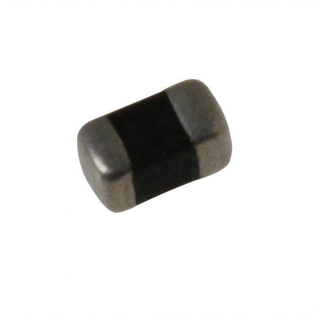
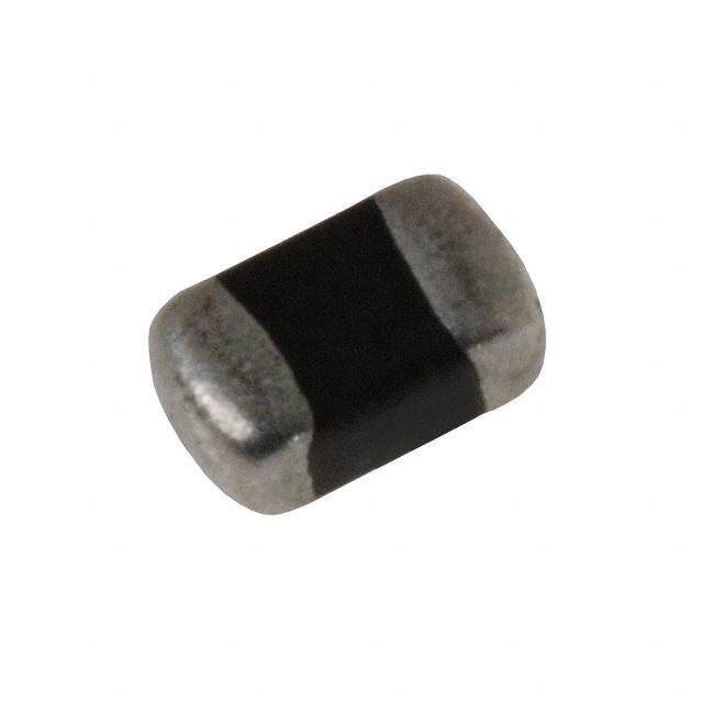
| 描述 | VARISTOR 23V 1206压敏电阻 23V Automotive |
| 产品分类 | |
| 品牌 | Littelfuse |
| 产品手册 | |
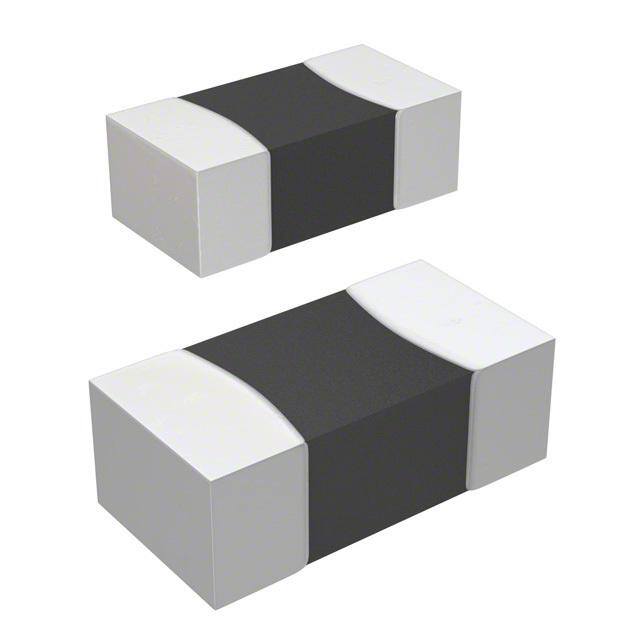
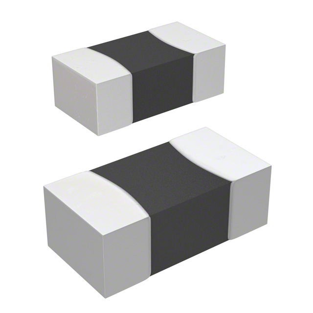
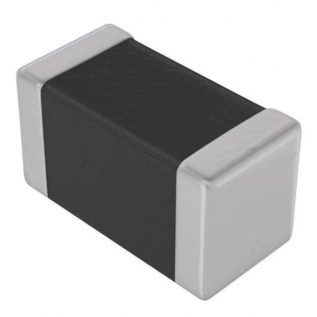
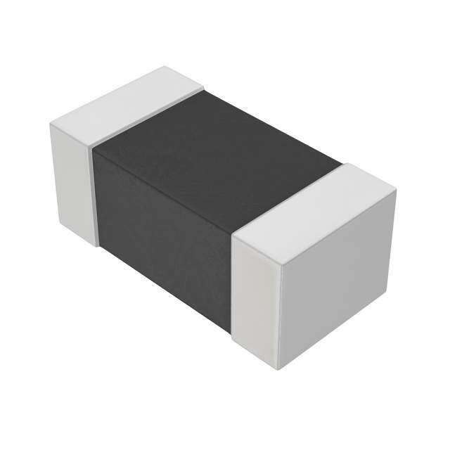
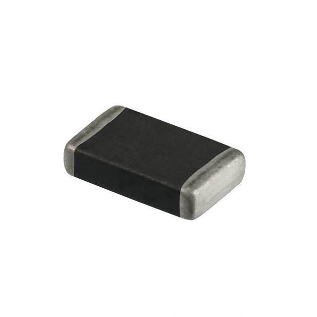
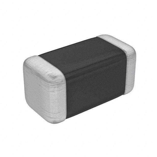
| 产品图片 |
|
| rohs | 符合RoHS不受无铅要求限制 / 符合限制有害物质指令(RoHS)规范要求 |
| 产品系列 | Littelfuse V18AUMLA1206NHAUML |
| 数据手册 | |
| 产品型号 | V18AUMLA1206NH |
| 产品 | MLV |
| 产品培训模块 | http://www.digikey.cn/PTM/IndividualPTM.page?site=cn&lang=zhs&ptm=25313 |
| 产品种类 | 压敏电阻 |
| 其它名称 | F3803TR |
| 包装 | 带卷 (TR) |
| 变阻器电压 | 23 V |
| 商标 | Littelfuse |
| 外壳代码-in | 1206 |
| 外壳代码-mm | 3216 |
| 外壳宽度 | 1.6 mm |
| 安装 | SMD/SMT |
| 宽度 | 1.6 mm |
| 封装 | Reel |
| 封装/外壳 | 1206(3216 公制) |
| 封装/箱体 | 1206 (3216 metric) |
| 尺寸 | 1.6 mm W x 3.2 mm L x 1.8 mm H |
| 峰值浪涌电流 | 1.5 A |
| 工作温度范围 | - 55 C to + 125 C |
| 工厂包装数量 | 2500 |
| 最大AC电压 | 14VAC |
| 最大DC电压 | 18VDC |
| 标准包装 | 2,500 |
| 浪涌能量额定值 | 1.5 J |
| 电压 | 18 VDC |
| 电压额定值DC | 18 V |
| 电流-浪涌 | - |
| 电路数 | 1 |
| 端接类型 | SMD/SMT |
| 系列 | AUML |
| 能量 | 1.5J |
| 钳位电压 | 40 V |


- 商务部:美国ITC正式对集成电路等产品启动337调查
- 曝三星4nm工艺存在良率问题 高通将骁龙8 Gen1或转产台积电
- 太阳诱电将投资9.5亿元在常州建新厂生产MLCC 预计2023年完工
- 英特尔发布欧洲新工厂建设计划 深化IDM 2.0 战略
- 台积电先进制程称霸业界 有大客户加持明年业绩稳了
- 达到5530亿美元!SIA预计今年全球半导体销售额将创下新高
- 英特尔拟将自动驾驶子公司Mobileye上市 估值或超500亿美元
- 三星加码芯片和SET,合并消费电子和移动部门,撤换高东真等 CEO
- 三星电子宣布重大人事变动 还合并消费电子和移动部门
- 海关总署:前11个月进口集成电路产品价值2.52万亿元 增长14.8%

PDF Datasheet 数据手册内容提取
Metal-Oxide Varistors (MOVs) Surface Mount Multilayer Varistors (MLVs) > AUML Series AUML Varistor Series RoHS Description The AUML Series of Multilayer Transient Surge Suppressors was specifically designed to suppress the destructive transient voltages found in an automobile. The most common transient condition results from large inductive energy discharges. The electronic systems in the automobile, e.g. antilock brake systems, direct ignition systems, engine control, airbag control systems, wiper motor controls, etc., are susceptible to damage from these voltage transients and thus require protection. The AUML transient suppressors have temperature independent suppression characteristics affording protection from -55ºC to 125ºC. The AUML suppressor is manufactured from semiconducting Size Table ceramics which offer rugged protection and excellent transient energy absorption in a small package. The devices Metric EIA are available in ceramic leadless chip form, eliminating lead inductance and assuring fast speed of response to transient 3216 1206 surges. These Suppressors require significantly smaller 3225 1210 space and land pads than Silicon TVS diodes, offering greater circuit board layout flexibility for the designer. 4532 1812 5650 2220 Also see the Littelfuse ML, MLN and MLE Series of Multilayer Suppressors. Applications Features • Suppression of MLN Series) • AEC - Q200 compliant • High peak surge inductive switching • Provides on-board • RoHS Compliant current capability or other transient transient voltage • Load Dump energy • Low Profile, compact events such as EFT protection for ICs rated per SAE industry standard chip and surge voltage at and transistors Specification J1113 size; (1206, 1210, 1812 the circuit board level and 2220 Sizes) • Used to help achieve • Leadless, surface • ESD protection for electromagnetic mount chip form • Inherent bidirectional components sensitive clamping compliance of • “Zero” Lead Inductance to IEC 61000-4-2 end products • No Plastic or epoxy (Level 4), MIL-STD- • Variety of energy packaging assures 883C, Method 3015.7, • Replace larger surface ratings available better than 94V-0 and other industry mount TVS Zeners in • No temperature derating flammability rating specifications (See many applications up to 125ºC ambient Also the MLE or Absolute Maximum Ratings • For ratings of individual members of a series, see Device Ratings and Specifications chart. Continuous AUML Series Units Steady State Applied Voltage: DC Voltage Range (V ) 18, 24, 48, 68 V M(DC) Transient: Load Dump Energy, (W ) 1.5 to 25 J LD Jump Start Capability (5 minutes), (V ) 48 V JUMP Operating Ambient Temperature Range (T ) -55 to +125 OC A Storage Temperature Range (T ) -55 to +150 OC STG Temperature Coefficient (αV) of Clamping Voltage (V ) at Specified Test Current <0.01 %/OC C CAUTION: Stresses above those listed in “Absolute Maximum Ratings” may cause permanent damage to the device. This is a stress only rating and operation of the device at these or any other conditions above those indicated in the operational sections of this specification is not implied. © 2017 Littelfuse, Inc. Specifications are subject to change without notice. Revised: 09/14/17
Metal-Oxide Varistors (MOVs) Surface Mount Multilayer Varistors (MLVs) > AUML Series Device Ratings and Specifications Maximum Ratings (125ºC) Specifications (25ºC) Maximum Jump Start Load Dump Nominal Varistor Voltage Maximum Maximum Clamping Continuous Voltage Energy at 10mA Standby Leakage Voltage (V ) at Part Number DC Voltage (5 Min) (10 Pulses) DC Test Current (at 13V DC) Test Current (C8/20µs) V V W V Min V Max I V I M(DC) JUMP LD N(DC) N(DC) L C P (V) (V) (J) (V) (V) (µA) (V) (A) V18AUMLA1206 18 24.5 1.5 23 32 50 40 1.5 V18AUMLA1210 18 24.5 3.0 23 32 50 40 1.5 V18AUMLA1812 18 24.5 6.0 23 32 100 40 5.0 V18AUMLA2220 18 24.5 25 23 32 200 40 10.0 V24AUMLA2220 24 24.5 25 32 39 200 60 10.0 V48AUMLA2220 48 24.5 25 54.5 66.5 200 105 10.0 V68AUMLA2220 68 24.5 25 77.2 94.4 200 135 10.0 NOTES: 1. Average power dissipation of transients not to exceed 0.1W, 0.15W, 0.3W and 1W for model sizes 1206, 1210, 1812 and 2220 respectively. 2. Load dump :min. time of energy input 40ms, interval 60sec(the load dump time constant Td differs from the time constant of energy input; load dump rating for ISO 7637-2 pulse 5a, please contact littelfuse. 3. Thermal shock capability per Mil-Std-750, Method 1051: -55ºC to 125ºC, 5 minutes at 25ºC, 25 Cycles: 15 minutes at each extreme. 4. For application specific requirements, please contact Littelfuse. Current, Energy and Power Derating Curve Peak Pulse Current Test Waveform for Clamping Voltage When transients occur in rapid succession, the average power dissipation is the energy (watt-seconds) per pulse 100 times the number of pulses per second. The power so UE L developed must be within the specifications shown on the A K V Device Ratings and Characteristics Table for the specific A E device. Certain parameter ratings must be derated at high F P 50 temperatures as shown below. T O N E C R 100 PE 0 T E 90 O1 TIME ATED VALU 876000 Fi1g00ure 2 MAXIMUM LETA1KAGE T2 MAXIMUM CLAMPING VOLTAGE 11281102/1206 F R 50 0 = Virtual Origin of Wave 2220 O 1 T 40 T = Time from 10% to 90% of Peak N PERCE 321000 VOLTAGE10 121F0TT/11I228G212012 260U==R RDEie s 2c e . a PFTyOEi mTARimKe C e=PLUA 1LM.2SP5EI N xCG TU RVROELTNATG TEEST WAVEFORM Example - For an 8/20 µs Current Waveform: 0 -55 50 60 70 80 90 100 110 120 130 140 150 O1 = VI8RµTUsA =L TO1R I=G IRN iOsFe W TAimVEe Figure 1 AMBIENT TEMPERATURE (oC) 1 t1t == TVIIM2R0ETU µFAsRL O= FM RT 1O20 N=%T TDTOIeM 9cE0a %=y 1 OT.2iF5m PxeE tAK MaximFuImGU RLEe a1.kaCCgUUeRR VRCEEuNrTr,e EnNtE/RCGlaYm ApNDin PgO VWoElRta DgEeR CATuINrvGe for Typicalt V2 -=10I µV (ICAMIRhPTUaULrA1aS0L0Ec µTA tIDMeUErRi TsA1OtmTi AIHcOsAN L)oFf 1V0 AmthCALUUeRER VE1N01T08mAAUM1ALA22120A0 at -14000AºC, AUML Series at 25ºC 25ºC, F8IGE5UXRºAEC 2M. MPaALnXEIMd:U M1 L2EA5KAºGCE CURRENT/CLAMPING VOLTAGE CURVE FOR AUML SERIES AT 25oC FOR AN 8/20 s CURRENT WAVEFORM 8 s = t1 = VIRTUAL FRONT TIME MAXIMUM LEAKAGE MAXIMUM CLAMPING VOLTAGE 100 20 s = t2 = VHIARLTFU AVALL TUIMEE TO 100 1210/1206 1812 2220 VOLTAGE10 1210/112282012260 VOLTAGE10 -4205ooCC 85oC 125oC 1 1 1µA 10µA 100µA 1mA 10mA 100mA 1A 10A 100A 1000A Figure 310µA 100µA 1mA 10mA 100mA 1A 10A 100A Figure 4 CURRENT CURRENT FIGURE 2.MAXIMUM LEAKAGE CURRENT/CLAMPING VOLTAGE CURVE FOR AUML SERIES AT 25oC FIGURE 3.TYPICAL V-I CHARACTERISTICS OF THE V18AUMLA2220 at -40oC, 25oC, 85oC AND 125oC © 2017 Littelfuse, Inc. Specifications are subject to change without notice. Revised: 09/14/17 100 OLTAGE10 -4205ooCC V 85oC 125oC 1 1µA 10µA 100µA 1mA 10mA 100mA 1A 10A 100A 1000A CURRENT FIGURE 3.TYPICAL V-I CHARACTERISTICS OF THE V18AUMLA2220 at -40oC, 25oC, 85oC AND 125oC
Metal-Oxide Varistors (MOVs) Surface Mount Multilayer Varistors (MLVs) > AUML Series Temperature Effects Speed of Response In the leakage region of the AUML suppressor, the device The clamping action of the AUML suppressor depends characteristics approaches a linear (ohmic) relationship on a conduction mechanism similar to that of other and shows a temperature dependent affect. In this region semiconductor devices (i.e. P-N Junctions). The apparent the suppressor is in a high resistance mode (approaching slow response time often associated with transient 106Ω) and appears as a near open-circuit. Leakage currents voltage suppressors (Zeners, MOVs) is often due to at maximum rated voltage are in the microamp range. parasitic inductance in the package and leads of the device and less dependent of the basic material (Silicon, When clamping transients at higher currents (at and above Z O). Thus, the single most critical element affecting the the 10mA range), the AUML suppressor approaches N response time of any suppressor is its lead induc-tance. a 1-10 characteristic. In this region the characteristics The AUML suppressor is a surface mount device, with no of the AUML are virtually temperature independent. leads or external packaging, and thus, it has virtually zero Figure 3 shows the typical effect of temperature on inductance. The actual response time of a AUML surge the V-I characteristics of the AUML suppressor. suppressor is in the 1 to 5 ns range, more than sufficient for the transients which are likely to be encountered in an Load Dump Energy Capability automotive environment. A Load Dump transient occurs when the alternator load in the automobile is abruptly reduced. The worst case Multilayer Internal Construction scenario of this transient occurs when the battery is disconnected while operating at full rated load. There are a number of different Load Dump specifications in existence in the automotive industry, with the most common one being that recommended by the Society of Automotive Engineers, specification #SAE J1113. Because of the diversity of these Load Dump specifications Littelfuse defines the Load Dump energy capability of the AUML suppressor range as that energy dissipated by the device itself, independent of the test circuit setup. The resultant Load Dump energy handling capability serves as an excellent figure of merit for the AUML Figure 5 suppressor. Standard Load Dump specifications require a device capability of 10 pulses at rated energy, across a temperature range of -40ºC to +125ºC. This capability AUML Load Dump Pulsing over a Temperature Range of requirement is well within the ratings of all of the AUML -55ºC to +125ºC Series (Figure 6 on next page). The very high energy absorption capability of the AUML V(10mA) suppressor is achieved by means of a highly controlled 35 2220 = 25J manufacturing process. This technology ensures that a 30 1812 = 6J large volume of suppressor material, with an interdigitated 1210 = 3J 25 layer construction, is available for energy absorption in an GE 20 extremely small package. Unlike equivalent rated Silicon LTA TVS diodes, the entire AUML device volume is available to VO 15 dissipate the Load Dump energy. 10 Hence, the peak temperatures generated by the Load 5 Dump transient are significantly lower and evenly 0 0 12 3 4 5 6 7 8 9 10 11 12 dissipated throughout the complete device (Figure 5 below). This even energy dissipation ensures that there Figure 6 # OF LOAD DUMPS FIGURE 5. AUML LOAD DUMP PULSING OVER A TEMPERATURE RANGE OF -55˚C TO 125˚C are lower peak temperatures generated at the P-N grain boundaries of the AUML suppressor. There are a number of different size devices available in the V(10mA) AUML Series, each one with a load dump energy rating, 35 2220 = 25J 1812 = 6J which is size dependent. 30 1210 = 3J 25 E G 20 A LT VO 15 10 © 2017 Littelfuse, Inc. Specifications are subject to change without notice. 5 Revised: 09/14/17 0 0 50 100 150 200 250 300 350 1,000 2,000 # OF LOAD DUMPS FIGURE 6. REPETITIVE LOAD DUMP PULSING AT RATED ENERGY V AT 10mA 100 E G A LT O V V18AUMLA2220 10 1000 2000 3000 4000 5000 6000 7000 NUMBER OF PULSES FIGURE 7. REPETITIVE ENERGY TESTING OF THE V18AUMLA2220 AT AN ENERGY LEVEL OF 2 JOULES
Metal-Oxide Varistors (MOVs) Surface Mount Multilayer Varistors (MLVs) > AUML Series Explanation of Terms Maximum Continuous DC Working Voltage (V ) M*(DC)++ This is the maximum continuous DC voltage which may be applied, up to the maximum operating temperature (125ºC), to the ML suppressor. This voltage is used as the reference test point for leakage current and is always less than the breakdown voltage of the device. Load Dump Energy Rating W LD+ This is the actual energy the part is rated to dissipate under Load Dump conditions (not to be confused with the "source energy" of a Load Dump test specification). Maximum Clamping Voltage V C+ This is the peak voltage appearing across the suppressor when measured at conditions of specified pulse current and specified waveform (8/20µs). It is important to note that the peak current and peak voltage may not necessarily be coincidental in time. Leakage Current I L+ In the nonconducting mode, the device is at a very high impedance (approaching 106Ω at its rated working voltage) and appears as an almost open circuit in the system. The leakage current drawn at this level is very low (<25µA at ambient temperature) and, unlike the Zener diode, the multilayer TVS has the added advantage that, when operated up to its maximum temperature, its leakage current will not increase above 500µA. Nominal Voltage V NDC++ This is the voltage at which the AUML enters its conduction state and begins to suppress transients. In the automotive environment this voltage is defined at the 10mA point and has a minimum (V ) and maximum (V ) voltage specified. N(DC) MIN N(DC) MAX Additional Information Datasheet Resources Samples © 2017 Littelfuse, Inc. Specifications are subject to change without notice. Revised: 09/14/17
Metal-Oxide Varistors (MOVs) Surface Mount Multilayer Varistors (MLVs) > AUML Series Lead (Pb) Soldering Recommendations The principal techniques used for the soldering of Reflow Solder Profile components in surface mount technology are IR Re-flow and Wave soldering. Typical profiles are shown on the right. The termination option available for each solder technique is: 230 Reflow Wave 230 1. Nickel Barrier (preferred) 1. Nickel Barrier (preferred) 2. Silver/Platinum The recommended solder for the AUML suppressor is a 62/36/2 (Sn/Pb/Ag), 60/40 (Sn/Pb) or 63/37 (Sn/Pb). Littelfuse also recommends an RMA solder flux. 230 Wave soldering is the most strenuous of the processes. To avoid the possibility of generating stresses due to Figure 9 thermal shock, a preheat stage in the soldering process FIGURE 8.REFLOW SOLDER PROFILE is recommended, and the peak temperature of the solder process should be rigidly controlled. Wave Solder PrFoIGfiURleE 8.REFLOW SOLDER PROFILE 300 When using a reflow process, care should be taken to ensure that the AUML chip is not subjected to a thermal 235000 MAXIMUM WAVE 260oC gradient steeper than 4 degrees per second; the ideal MAXIMUM WAVE 260oC gprraodcieesnst, bpereinhge 2at idnegg troe ewsi tpheinr s1e0c0o dnedg. rDeuersin ogf tthhee ssoollddeerri'nsg oRE (C)C)222050000 FIGURE 8.REFLOW SOLDER PROFILE oU150 peak temperature is essential to minimize thermal shock. RATRE ( SECOND PREHEAT Once the soldering process has been completed, it TEMPEMPERATU13110505000000 FIRST PMRAEXHIEMAUSTMEC WOANVDE P2R60EoHCEAT is still necessary to ensure that any further thermal E250 T FIRST PREHEAT sshhoocckks i sa rheo ta vporiindteedd. cOirnceu ipt obsosaibrdles cbaeuinsge roefm thoevremd aflr om oE (C)20500000.0 0.5 1.0 1.5TIM2E. 0(MINU2.T5ES)3.0 3.5 4.0 4.5 the solder process and subjected to cleaning solvents UR1500.0 0.5 1.0 1.5 2.0 2.5 3.0 3.5 4.0 4.5 Figure 1AT0 FIGURE 9.WATVIMEE S (MOSILNEDCUEOTERNSD P) PRROEFHIELAET at room temperature. The boards must be allowed to R E P100 cool gradually to less than 50ºC before cleaning. M FIGURE 9.WAVE SOLDER PROFILE E T FIRST PREHEAT 50 0 MAXIMUM TEMPERATURE 260˚C Lead–free (Pb-free) Soldering Recommendations 0.0 0.520 - 41.00 SEC1O.5NDS 2W.0ITHIN2 .55˚C 3.0 3.5 4.0 4.5 MAXIMUM TEMTPIMEER (AMTIUNRUETE 2S6)0˚C 20 - 40 SECONDRSA WMPIT HRIANT E5˚C Littelfuse offers the Nickel Barrier Termination finish for the FIGURE 9.WA<V3E˚C S/sOLDER PRO6F0IL - E150 SEC Lead–free Re-flow SolderR PAMroP RfiAlTeE > 217˚C optimum Lead–free solder performance. <3˚C/s 60 - 150 SEC > 217˚C The preferred solder is 96.5/3.0/0.5 (SnAgCu) with an RMA PREHEAT ZONE flux, but there is a wide selection of pastes and fluxes MAXIMUM TEMPERATURE 260˚C available with which the Nickel Barrier parts should be 20 P- R4E0 HSEEACTO ZNODNSE WITHIN 5˚C compatible. RAMP RATE <3˚C/s 5.600 - 1 5 0 6 S.0E C 7.0 > 217˚C The reflow profile must be constrained by the maximums 5.0 6.0 7.0 in the Lead–free Reflow Profile. For Lead–free Wave FIGURE 10. LEAD-FREE RE-FLOW SOLDER PROFILE soldering, the Wave Solder Profile still applies. FIGURE P1R0E.HLEEAATD Z-OFRNEEE RE-FLOW SOLDER PROFILE Note: the Lead–free paste, flux and profile were used for evaluation purposes by Littelfuse, based upon industry standards and practices. There are multiple choices of all 5.0 6.0 7.0 Figure 11 three available, it is advised that the customer explores the optimum combination for their process as processes vary FIGURE 10. LEAD-FREE RE-FLOW SOLDER PROFILE considerably from site to site. © 2017 Littelfuse, Inc. Specifications are subject to change without notice. Revised: 09/14/17
Metal-Oxide Varistors (MOVs) Surface Mount Multilayer Varistors (MLVs) > AUML Series Product Dimensions (mm) PAD LAYOUT DIMENSIONS CHIP LAYOUT DIMENSIONS E Note: Avoid metal runs in this area, parts are not recommended for use in applications using silver (Ag) expoxy paste. L D W Note: Avoid metal runs in this area, parts are not recommended for use in applications using Silver (Ag) epoxy paste. 1206 Size 1210 Size 1812 Size 2220 Size SYMBOL IN MM IN MM IN MM IN MM A 0.203 5.150 0.219 5.510 0.272 6.910 0.315 8.000 B 0.103 2.620 0.147 3.730 0.172 4.360 0.240 6.190 C 0.065 1.650 0.073 1.850 0.073 1.850 0.073 1.850 D (max.) 0.071 1.80 0.070 1.80 0.07 1.80 0.118 3.00 0.50 -/+ E 0.020 -/+ 0.010 0.50 -/+0.25 0.020 -/+ 0.010 0.50 -/+ 0.25 0.020 -/+ 0.010 0.030 -/+ 0.010 0.75 -/+ 0.25 0.25 4.50 -/+ L 0.125 -/+ 0.012 3.20 -/+ 0.03 0.125 -/+ 0.012 3.20 -/+ 0.30 0.180 -/+ 0.014 0.225 -/+ 0.016 5.70 -/+ 0.40 0.35 3.20 -/+ W 0.060 -/+ 0.011 1.60 -/+ 0.28 0.100 -/+ 0.012 2.54 -/+ 0.30 0.125 -/+ 0.012 0.197 -/+ 0.016 5.00 -/+ 0.40 0.30 Part Numbering System V 18 AUML A 2220 X X PACKING OPTIONS DEVICE FAMILY A: Bulk Pack, 2500 pieces TVSS Device H: 7in (178mm) Diameter Reel* T: 13in (330mm) Diameter Reel* MAXIMUM DC WORKING VOLTAGE * See quanttities in Packaging table below END TERMINATION OPTION AUTOMOTIVE N or No Letter: Nickel Barrier MULTILAYER DESIGNATOR LOAD DUMP ENERGY RATING DEVICE SIZE INDICATOR i.e., 220 mil x 200 mil Packaging* Quantity Device Size 13” Inch Reel 7” Inch Reel Bulk Pack ('T' Option) ('H' Option) ('A' Option) 1206 10,000 2,500 2,500 1210 8,000 2,000 2,000 1812 4,000 1,000 1,000 2220 4,000 1,000 1,000 *(Packaging) It is recommended that parts be kept in the sealed bag provided and that parts be used as soon as possible when removed from bags. © 2017 Littelfuse, Inc. Specifications are subject to change without notice. Revised: 09/14/17
Metal-Oxide Varistors (MOVs) Surface Mount Multilayer Varistors (MLVs) > AUML Series Tape and Reel Specifications Symbol Description Dimensions in Millimeters A Width of Cavity Dependent on Chip Size to Minimize Rotation. 0 B Length of Cavity Dependent on Chip Size to Minimize Rotation. 0 K Depth of Cavity Dependent on Chip Size to Minimize Rotation. 0 W Width of Tape 8 -/+ 0.2 12 -/+ 0.2 F Distance Between Drive Hole Centers and Cavity Centers 3.5 -/+ 0.5 5.4 -/+ 0.5 E Distance Between Drive Hole Centers and Tape Edge 1.75 -/+ 0.1 1.75 -/+ 0.1 P Distance Between Cavity Center 4 -/+ 0.1 8-/+ 0.1 1 P Axial Distance Between Drive Hole Centers and Cavity Centers 2 -/+ 0.1 2 -/+ 0.1 2 P Axial Distance Between Drive Hole Centers 8 -/+ 0.1 8 -/+ 0.1 0 D Drive Hole Diameter 1.55 -/+ 0.05 1.55 -/+ 0.05 0 D Diameter of Cavity Piercing 1.05 -/+ 0.05 1.55 -/+ 0.05 1 T Embossed Tape Thickness 0.3 Max 0.4 Max 1 T Top Tape Thickness 0.1 Max 0.1 Max 2 NOTE: Dimensions in millimeters. • Conforms to EIA-481-1, Revision A • Can be supplied to IEC publication 286-3 Tape 8mm Wide Tape 12mm Wide Tape Chip Size 1206 1210 1812 2220 Standard Packaging Special Packaging Tape and reel is the standard packaging method of the Option1: 178 millimeter (7–inch) reels containing 1000 AUML Series. The standard 300 millimeter (13–inch) reel (2220, 1812), 2000 (1210), 2500 (1206), pieces utilized contains 4000 pieces for the 2200 and 1812 chips, are available. To order add 'H' to the standard 8000 pieces for the 1210 chip and 10,000 pieces for the part number, e.g. V18AUMLA2220H. 1206 size. Option 2 For small sample quantities (less than 100 To order: add 'T' to the standard part number, pieces) the units are shipped bulk pack. To e.g.V18AUMLA222OT. order add 'A' to the standard part number, e.g. V18AUMLA2220A. Disclaimer Notice - Information furnished is believed to be accurate and reliable. However, users should independently evaluate the suitability of and test each product selected for their own applications. Littelfuse products are not designed for, and may not be used in, all applications. Read complete Disclaimer Notice at www.littelfuse.com/disclaimer-electronics. © 2017 Littelfuse, Inc. Specifications are subject to change without notice. Revised: 09/14/17