ICGOO在线商城 > 电路保护 > TVS - 变阻器,MOV > AVR-M2012C120MT6AB
 Datasheet下载
- 型号: AVR-M2012C120MT6AB
- 制造商: TDK
- 库位|库存: xxxx|xxxx
- 要求:
| 数量阶梯 | 香港交货 | 国内含税 |
| +xxxx | $xxxx | ¥xxxx |
查看当月历史价格
查看今年历史价格
AVR-M2012C120MT6AB产品简介:
ICGOO电子元器件商城为您提供AVR-M2012C120MT6AB由TDK设计生产,在icgoo商城现货销售,并且可以通过原厂、代理商等渠道进行代购。 AVR-M2012C120MT6AB价格参考。TDKAVR-M2012C120MT6AB封装/规格:TVS - 变阻器,MOV, 12V 60A Varistor 1 Circuit Surface Mount, MLCV 0805 (2012 Metric)。您可以下载AVR-M2012C120MT6AB参考资料、Datasheet数据手册功能说明书,资料中有AVR-M2012C120MT6AB 详细功能的应用电路图电压和使用方法及教程。
TDK Corporation的AVR-M2012C120MT6AB是一款多层压敏电阻(MOV),主要用于电路中的瞬态电压抑制,提供过电压保护。其应用场景主要包括以下几个方面:

1. 消费类电子产品:如智能手机、平板电脑、笔记本电脑等,用于保护敏感电子元件免受静电放电(ESD)和瞬态电压的损害。

2. 通信设备:在路由器、交换机、基站等通信设备中,用于保护接口电路,防止因雷击或电源波动引起的电压浪涌。

3. 工业控制系统:用于PLC、传感器、工业计算机等设备中,提供可靠的过电压保护,确保系统稳定运行。

4. 汽车电子:应用于车载电子系统,如车载信息娱乐系统、驾驶辅助系统等,保护电路免受车辆电气系统中可能产生的电压尖峰影响。

5. 家电产品:如空调、洗衣机、微波炉等,用于保护控制电路和电源模块,提升产品安全性和可靠性。

该器件具有小型化、响应速度快、可靠性高等特点,适用于高密度电子组装环境,符合RoHS标准,适合SMT工艺。
| 参数 | 数值 |
| 产品目录 | |
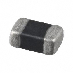
| 描述 | VARISTOR 12V 60A 0805压敏电阻 0805 12V 60A 1000pF |
| 产品分类 | |
| 品牌 | TDK Corporation |
| 产品手册 | |
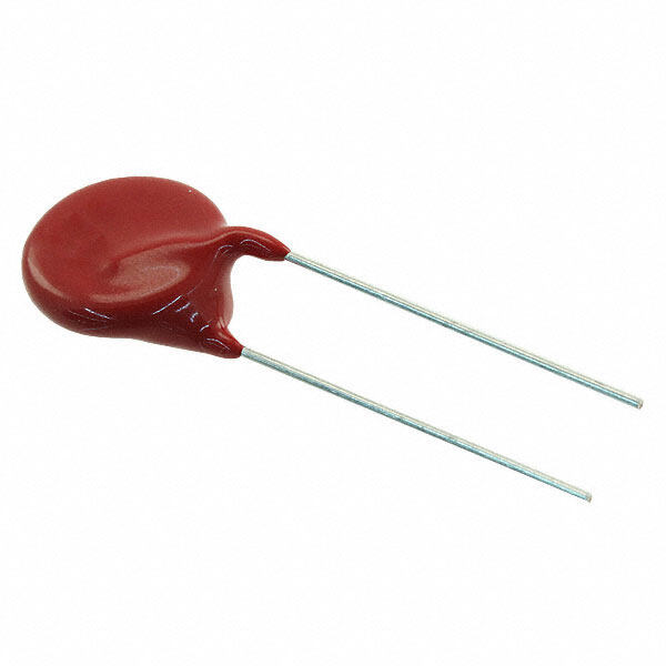
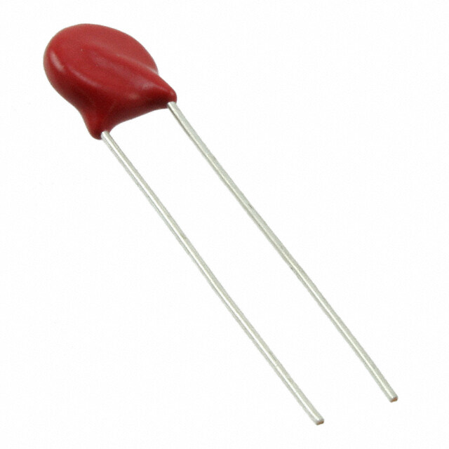
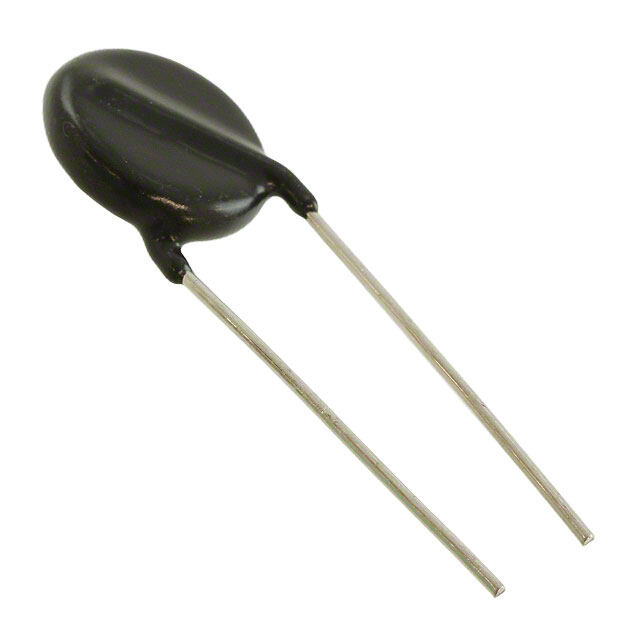
| 产品图片 |
|
| rohs | 符合RoHS无铅 / 符合限制有害物质指令(RoHS)规范要求 |
| 产品系列 | TDK AVR-M2012C120MT6ABAVR-M |
| 数据手册 | |
| 产品型号 | AVR-M2012C120MT6AB |
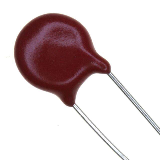
| 产品目录绘图 |
|
| 产品目录页面 | |
| 产品种类 | 压敏电阻 |
| 其它名称 | 445-2547-6 |
| 包装 | Digi-Reel® |
| 变阻器电压 | 12V |
| 商标 | TDK |
| 外壳代码-in | 0805 |
| 外壳代码-mm | 2012 |
| 安装 | SMD/SMT |
| 封装 | Reel |
| 封装/外壳 | 0805(2012 公制) |
| 封装/箱体 | 0805 (2012 metric) |
| 尺寸 | 2 mm L |
| 峰值浪涌电流 | 60 A |
| 工作温度范围 | - 40 C to + 125 C |
| 工厂包装数量 | 2000 |
| 最大AC电压 | - |
| 最大DC电压 | 7.5VDC |
| 标准包装 | 1 |
| 浪涌能量额定值 | 0.2 J |
| 电压额定值DC | 7.5 V |
| 电容 | 1000 pF |
| 电流-浪涌 | 60A |
| 电路数 | 1 |
| 端接类型 | SMD/SMT |
| 能量 | 0.20J |
| 钳位电压 | 20 V |


- 商务部:美国ITC正式对集成电路等产品启动337调查
- 曝三星4nm工艺存在良率问题 高通将骁龙8 Gen1或转产台积电
- 太阳诱电将投资9.5亿元在常州建新厂生产MLCC 预计2023年完工
- 英特尔发布欧洲新工厂建设计划 深化IDM 2.0 战略
- 台积电先进制程称霸业界 有大客户加持明年业绩稳了
- 达到5530亿美元!SIA预计今年全球半导体销售额将创下新高
- 英特尔拟将自动驾驶子公司Mobileye上市 估值或超500亿美元
- 三星加码芯片和SET,合并消费电子和移动部门,撤换高东真等 CEO
- 三星电子宣布重大人事变动 还合并消费电子和移动部门
- 海关总署:前11个月进口集成电路产品价值2.52万亿元 增长14.8%

PDF Datasheet 数据手册内容提取
V o l t a g e P r o t e c t i o n D e v i c e s September 2014 Chip Varistors Countermeasure for surge voltage and static electricity AVR series AVRM0402/AVRL0402 0402 [01005 inch]* AVRM0603/AVRL0603 0603 [0201 inch] AVRM1005/AVRL1005 1005 [0402 inch] AVRM1608/AVRL1608 1608 [0603 inch] AVRM2012 2012 [0805 inch] * Dimensions Code JIS[EIA]
(2/26) Voltage Protection Devices REMINDERS FOR USING THESE PRODUCTS Before using these products, be sure to request the delivery specifications. SAFETY REMINDERS Please pay sufficient attention to the warnings for safe designing when using these products. REMINDERS Please observe the following precautions in order to avoid problems with chip varistors such as characteristic degradation and element destruction. Please store these products in an environment with a temperature of 5 to 40°C and humidity level of 20 to 70%RH, and use them within six months. Poor storage conditions may lead to the deterioration of the solderability of the edge electrodes, so please be careful to avoid contact with humidity, dew condensation, dust, toxic gas (hydrogen, hydrogen sulfide, sulfurous acid, chlorine, ammonia, etc.), direct sunlight, and so on. Please do not use products that have been dropped or detached when mounting. Please solder with the reflow soldering method, and not the flow (dip) soldering method. Please observe the following precautions to avoid problems with varistors such as characteristic degradation and element destruction, which ultimately lead to the generation of heat and smoke with the elements. Do not use in locations where the temperatures exceed the operating temperature range such as under direct sunlight or near sources of heat. Do not use in locations where there are high levels of humidity such as under direct exposure to weather and areas where steam is released. Do not use in locations such as dusty areas, high-saline environments, places where the atmosphere is contaminated with corrosive gas, etc. Avoid powerful vibrations, impact (such as by dropping), pressure, etc. that may lead to splitting in the products. Do not use with a voltage that exceeds the maximum allowable circuit voltage. When resin coating (including modular) a varistor, do not use a resin that will cause deterioration of the varistor. Be sure never to use resin that generates hydrogen as palladium is used for the inner electrode. Avoid attachment near combustible materials. Please contact our sales offices when considering the use of the products listed on this catalog for applications, whose performance and/or quality require a more stringent level of safety or reliability, or whose failure, malfunction or trouble could cause serious damage to society, person or property ('specific uses' such as automobiles, airplanes, medical instruments, nuclear devices, etc.) as well as when considering the use for applications that exceed the range and conditions of this catalog. Please also contact us when using these products for automotive applications. Please note that we are not responsible for any damages or losses incurred resulting from the use of these products that exceeds the range and conditions of this catalog or specific uses. Please take appropriate measures such as acquiring protective circuits and devices that meet the uses, applications, and conditions of the instruments and keeping backup circuits. 20140922 / vpd_varistors_avr_en.fm
(3/26) Voltage Protection Devices Chip Varistors Product compatible with RoHS directive Compatible with lead-free solders Countermeasure for surge voltage and static electricity Overview of the AVR Series CHARACTERISTICS OF CHIP VARISTOR Varistors are voltage dependent nonlinear resistive elements with a resistance that decreases rapidly when the voltage is over the constant value. Varistor is equivalent with Zener diode of two series connection. Therefore, do not have polarity. CURRENT vs. VOLTAGE CHARACTERISTICS EQUIVALENT CIRCUIT 2 Zener Diodes )A 10–1 (nt 10–2 Zener diode Curre Positive direction 1100––34 /Vz:6.8V C/Vh1imp Av:a1r2isVtor A capacitance content 10–5 –18 –14 –10 –6 –2 2 6 10 14 18 –10–5 –10–4 –10–3 Negative direction –10–2 –10–1 Voltage(V) THE EFFECT OF THE VARISTOR Without Varistor With Varistor A malfunction and failure of electronic equipment Suppress abnormal voltage by inserting varistor in a circuit ESD, Surge voltage ESD, Surge voltage IC IC Power line Power line Signal line Signal line Insert a varistor between a line and ground : Chip varistor RoHS Directive Compliant Product: See the following for more details related to RoHS Directive compliant products. http://product.tdk.com/en/environment/rohs/ • All specifications are subject to change without notice. 20140922 / vpd_varistors_avr_en.fm
(4/26) Voltage Protection Devices Overview of the AVR Series MEASURING CIRCUIT Sample IC USB2.0 Test board on board PC Test set : Chip varistor Without Varistor With Varistor AVRL101A3R3FTA (3.3pF) AVRL101A6R8GTA (6.8pF) MERITS OF REPLACEMENT FROM ZENER DIODE (1) Reduction in the Number of Parts Production examples Zener diode+capacitor Chip varistor Example of replacement at audio terminal Audio Audio Audio/out connector Audio/out connector Audio Audio AMP AMP : Chip varistor (2) Improved Electrostatic Absorption Capability Compare data of chip varistor and zener diode about IC protection ESD measurements of CMOS-ICs with AVR-type varistors and zener diodes 10–7 ation resistance Ω()ested circuit 111000–––456 With Zener Diode AVR-M1608C120MT6AB nsulof t I 10–3 0 2 4 6 8 10 12 14 ESD voltage(kV) CMOS: D74HC04C ESD generator : Noise Laboratory Co.,Ltd., ESS -630A 200pF-0Ω method model equipment Contact type discharge ESD applied point: Vcc-ground • All specifications are subject to change without notice. 20140922 / vpd_varistors_avr_en.fm
(5/26) Voltage Protection Devices Overview of the AVR Series FEATURES No polarity, due to symmetrical current-voltage characteristics. Equivalent to anode common type Zener diode. Excellent electrostatic absorption capability. Response is as good or better than Zener diode.Keeps symmetrical current-voltage characteristics even after electrostatic absorption. Adopted the inner electrodes lamination structure. • Wide range of varistor voltages are available in series (6.8 to 90V). • Low capacitance items are available in series (from 1.1pF). • World’s smallest 0402-, 0603-, 1005-, 1608-, 2012-chip size are available in series. Excellent mount reliability. Good for Pb-free soldering.Adopted (Ni/Sn) electroplating. Achieved good solderability and solder heat resistance. Can replace a Zener diode + capacitor combination. Reduced footprint and total mounting cost. APPLICATION Electrostatic absorption Pulse noise absorption APPLICATION EXAMPLES Consumer product Application Mobile phone Data terminal Digital video camera LCD panel Digital camera Touch panel PDA Button and switch unit Note PC Battery terminal DVD-ROM, CD-ROM Audio-Video input-output terminal CD/MD/MP3 player Microphone/receiver unit Game machine Controller unit CAN-BUS ECU Connector In-car equipment Air conditioner panel Car audio Car navigation SMART PHONE AUDIO, VIDEO To LCD driver Monitor Video1 Video2 Video3 Video5 OUT in in in in Microphone/Receiver LCD panel Digi Video Video Video Video LL/MONO L/MONO L/MONO L/MONO Button Data terminal : Chip varistor Audio Audio Audio Audio Audio USB2.0 R VDD USB cable D– USB IC D+ : Chip varistor USB connector F.G. : Chip varistor • All specifications are subject to change without notice. 20140922 / vpd_varistors_avr_en.fm
(6/26) Voltage Protection Devices Overview of the AVR Series PART NUMBER CONSTRUCTION AVRM 1005 C 6R8 N T 101 N Varistor Varistor voltage Capacitance or Capacitance Series name L×W Dimensions Structure voltage tolerance Packaging style TDK internal tolerance(cid:2) (mm) code (V) (%) code (%) 0402 0.4×0.2 6R8 6.8 K ±10 T Taping M ±20 0603 0.6×0.3 270 27 M ±20 B Bulk N ±30 1005 1.0×0.5 N ±30 1608 1.6×0.8 2012 2.0×1.2 (cid:2)(cid:3)When the capacitance is not included in the part number, the capacitance tolerance is also not described. AVRL 10 1A 3R3 F T A Maximum Capacitance L×W Dimensions Capacitance Varistor voltage or Series name continuous voltage tolerance Packaging style (mm) (pF) TDK internal code (Vdc) (pF) 04 0.4×0.2 1A 10 1R1 1.1 D ±0.5 T Taping 06 0.6×0.3 1C 16 2R2 2.2 F ±1 10 1.0×0.5 1E 25 3R3 3.3 G ±2 16 1.6×0.8 6R8 6.8 N ±0.3 OPERATING TEMPERATURE RANGE, PACKAGE QUANTITY, PRODUCT WEIGHT Temperature range Operating Storage Package quantity Individual weight Type temperature(cid:2) temperature(cid:2)(cid:2) (°C) (°C) (pieces/reel) (mg)typ. AVRM0402 –40 to +85 –40 to +85 20,000 0.1 AVRL0402 –40 to +85 –40 to +85 20,000 0.1 AVRM0603 –40 to +85 –40 to +85 15,000 0.2 AVRL0603 –40 to +85 –40 to +85 15,000 0.2 AVRM1005 –40 to +125 –40 to +125 10,000 1.2 AVRL1005 –40 to +85 –40 to +85 10,000 1.2 AVRM1608 –40 to +125 –40 to +125 4,000 5 AVRL1608 –40 to +85 –40 to +85 4,000 5 AVRM2012 –40 to +125 –40 to +125 2,000 12 (cid:2)(cid:3)Operating temperature range includes self-temperature rise. (cid:2)(cid:2)(cid:3)The Storage temperature range is for after the circuit board is mounted. OPERATIONAL VOLTAGE RANGES AVRM0402/AVRL0402 types 25 AVRM0603/AVRL0603 types 25 AVRM1005/AVRL1005 types 19 AVRM1608/AVRL1608 types 28 AVRM2012 type 28 0 5 10 15 20 25 30 Circuit voltage(V) • All specifications are subject to change without notice. 20140922 / vpd_varistors_avr_en.fm
(7/26) Voltage Protection Devices Overview of the AVR Series TERMINOLOGY Item Unit Terminology Varistor voltage V1mA Voltage measured across the varistor when DC1mA is applied. (Breakdown voltage) (V) Maximum continuous voltage Vdc Maximum DC voltage that can be applied continuously. (Rated voltage) (V) Varistor leakage current: 50μA max. (Within the range of maximum allowable circuit voltage) Vcl Clamping voltage Voltage appearing across the varistor when a pulse current (8/20μs(cid:2)1) of specified peak value is applied. (V) E Maximum energy that can be absorbed without deteriorating varistor characteristics when an impulse Maximum energy (Joule) current (10/1000μs(cid:2)2) is applied once. Ip Maximum current that can be withstood without deteriorating varistor characteristics when an impulse Maximum peak current (A) current (8/20μs(cid:2)1) is applied once. C Capacitance measured at 1kHz Capacitance (pF) (or 1MHz) of oscillator frequency and 1Vrms of oscillator voltage. Rdc Insulation resistance Insulation resistance appearing across the varistor when specified voltage is applied. (M(cid:4)) (cid:2)1 8/20μs test waveform 100% 90% nt urre50% C 8μs 20μs Time (cid:2)2 10/1000μs test waveform 100% 90% gy er50% n E 10μs 1000μs Time • All specifications are subject to change without notice. 20140922 / vpd_varistors_avr_en.fm
(8/26) Voltage Protection Devices Overview of the AVR Series RECOMMENDED REFLOW PROFILE Preheating Soldering Natural cooling Peak T4 e ur T3 T3 at er p m e T T2 T: t3 T1 t1 t2 t: Time Preheating Soldering Peak Temp. Time Temp. Time Temp. Time T1 T2 t1 T3 t2 T4 t3 150°C 180°C 120s max. 230°C 40s max. 260°C max. 5s • All specifications are subject to change without notice. 20140922 / vpd_varistors_avr_en.fm
(9/26) Voltage Protection Devices AVR series AVRM0402/AVRL0402 Types SHAPE & DIMENSIONS INTERNAL STRUCTURE 0.4±0.02 Inner electrode Varistor body (Palladium) (Zinc Oxide: ZnO semiconductor ceramics) 02 Sn plating 0. ± 2 Ag termination 0. underlayer Ni plating 0.07 min. 2 0 0. ± 2 0. Dimensions in mm RECOMMENDED LAND PATTERN CIRCUITS DIAGRAM 2 0. o 8 t 1 0. 0.15 to 0.2 0.2 0.15 to 0.2 • All specifications are subject to change without notice. 20140922 / vpd_varistors_avr_en.fm
(10/26) Voltage Protection Devices AVR AVRM0402/AVRL0402 Types series ELECTRICAL CHARACTERISTICS CHARACTERISTICS SPECIFICATION TABLE AVRM0402 Varistor voltage Maximum continuous Clamping Maximum Maximum Capacitance (Breakdown voltage) voltage voltage energy peak current (Rated voltage) Part No. V1mA(V) Vdc(V) Vcl(V) E(Joule) Ip(A) C(pF) [DC1mA] [8/20μs] [10/1000μs] [8/20μs] [1kHz, 1Vrms] max. max. max. typ. AVRM0402C6R8NT101N 6.8 (4.76 to 8.84) 3.5 15[1A] 0.01 4 100 (70 to 130) AVRM0402C120MT330N 12 (9.6 to 14.4) 5.5 20[1A] 0.005 1 33 (23.1 to 43.9) AVRL0402 Varistor voltage Maximum continuous Capacitance Insulation voltage resistance (Rated voltage) Part No. V1mA(V) Vdc(V) C(pF) Rdc(M(cid:4)) [DC1mA] max. [1MHz, 1Vrms] [3Vrms] typ. min. AVRL041E1R1NTA 39 25 1.1[0.8 to 1.4] 10 • All specifications are subject to change without notice. 20140922 / vpd_varistors_avr_en.fm
(11/26) Voltage Protection Devices AVR AVRM0402/AVRL0402 Types series ELECTRICAL CHARACTERISTICS CURRENT vs. VOLTAGE CHARACTERISTICS IMPEDANCE vs. FREQUENCY CHARACTERISTICS 100 1000000 10–1 100000 10–2 10000 V1mA=6.8V V1mA=12V V1mA=39V Ω) )A10–3 (e1000 (Current10–4 peadanc 100 1.1pF m I 33pF 100pF 10–5 10 10–6 1 10–7 0.1 0 10 20 30 40 50 1 10 100 1000 10000 Voltage(V) Frequency(MHz) TRANSMISSION CHARACTERISTICS CAPACITANCE vs. FREQUENCY CHARACTERISTICS 10 1000 1.1pF 0 –10 100 100pF ()n lossdB –20 100pF 33pF ()ancepF 10 33pF Insertio –30 Capacit –40 1.1pF 1 –50 –60 0.1 1 10 100 1000 10000 1 10 100 1000 10000 Frequency(MHz) Frequency(MHz) • All specifications are subject to change without notice. 20140922 / vpd_varistors_avr_en.fm
(12/26) Voltage Protection Devices AVR series AVRM0603/AVRL0603 Types SHAPE & DIMENSIONS INTERNAL STRUCTURE 0.6±0.03 Inner electrode Varistor body (Palladium) (Zinc Oxide: ZnO semiconductor ceramics) 03 Sn plating 0. ± 3 Ag termination 0. underlayer Ni plating 0.1 min. 3 0 0. ± 3 0. Dimensions in mm RECOMMENDED LAND PATTERN CIRCUITS DIAGRAM 5 3 0. o 5 t 2 0. 0.2 to 0.3 0.25 to 0.35 0.2 to 0.3 • All specifications are subject to change without notice. 20140922 / vpd_varistors_avr_en.fm
(13/26) Voltage Protection Devices AVR AVRM0603/AVRL0603 Types series ELECTRICAL CHARACTERISTICS CHARACTERISTICS SPECIFICATION TABLE AVRM0603 Varistor voltage Maximum Clamping Maximum Maximum Capacitance (Breakdown voltage) continuous voltage voltage energy peak current (Rated voltage) Part No. V1mA(V) Vdc(V) Vcl(V) E(Joule) Ip(A) C(pF) [DC1mA] [8/20μs] [10/1000μs] [8/20μs] [1kHz, 1Vrms] max. max. max. typ. AVRM0603C6R8NT331N 6.8 ( 4.76 to 8.84) 3.5 14[1A] 0.02 16 330 (231 to 429) AVRM0603C6R8NT101N 6.8 ( 4.76 to 8.84) 3.5 14[1A] 0.01 10 100 ( 70 to 130) AVRM0603C080MT101N 8 ( 6.4 to 9.6) 5.5 17[1A] 0.01 4 100 ( 70 to 130) AVRM0603C120MT101N 12.8 (10 to 15.6) 5.5 20[1A] 0.01 5 100 ( 70 to 130) AVR-M0603C120MTAAB 12 ( 9.6 to 14.4) 7.5 23[1A] 0.01 1 33 AVRM0603C120MT150N 12.8 (10 to 15.6) 5.5 35[1A] 0.003 1 15 ( 10.5 to 19.5) AVRM0603C200MT150N 20 (16.0 to 24.0) 12 40[1A] 0.01 1 15 ( 10.5 to 19.5) [1MHz] AVRL0603 Varistor voltage Maximum continuous Capacitance Insulation voltage resistance (Rated voltage) Part No. V1mA(V) Vdc(V) C(pF) Rdc(M(cid:4)) [DC1mA] max. [1MHz, 1Vrms] [3Vrms] typ. min. AVRL061E1R1NTA 39 25 1.1[0.8 to 1.4] 10 • All specifications are subject to change without notice. 20140922 / vpd_varistors_avr_en.fm
(14/26) Voltage Protection Devices AVR AVRM0603/AVRL0603 Types series ELECTRICAL CHARACTERISTICS CURRENT vs. VOLTAGE CHARACTERISTICS IMPEDANCE vs. FREQUENCY CHARACTERISTICS 100 1000000 10–1 100000 10–2 10000 V1mA=6.8V V1mA=12V Ω) )A10–3 V1mA=39V (e1000 15pF (Current10–4 peadanc 100 33pF 1.1pF m I 100pF 10–5 10 10–6 1 10–7 0.1 0 10 20 30 40 50 1 10 100 1000 10000 Voltage(V) Frequency(MHz) TRANSMISSION CHARACTERISTICS CAPACITANCE vs. FREQUENCY CHARACTERISTICS 10 1000 0 1.1pF –10 100 100pF ()ossdB –20 ()cepF 1353ppFF n l 15pF an 10 Insertio –30 100pF 33pF Capacit –40 1.1pF 1 –50 –60 0.1 1 10 100 1000 10000 1 10 100 1000 10000 Frequency(MHz) Frequency(MHz) • All specifications are subject to change without notice. 20140922 / vpd_varistors_avr_en.fm
(15/26) Voltage Protection Devices AVR series AVRM1005/AVRL1005 Types SHAPE & DIMENSIONS INTERNAL STRUCTURE 1.0±0.05 Inner electrode Varistor body (Palladium) (Zinc Oxide: ZnO semiconductor ceramics) 05 Sn plating 0. ± 5 Ag termination 0. underlayer Ni plating 0.1 min. 5 0 0. ± 5 0. Dimensions in mm RECOMMENDED LAND PATTERN CIRCUITS DIAGRAM 6 0. o 4 t 0. 0.35 to 0.45 0.3 to 0.5 0.35 to 0.45 • All specifications are subject to change without notice. 20140922 / vpd_varistors_avr_en.fm
(16/26) Voltage Protection Devices AVR AVRM1005/AVRL1005 Types series ELECTRICAL CHARACTERISTICS CHARACTERISTICS SPECIFICATION TABLE AVRM1005 Varistor voltage Maximum continuous Clamping Maximum Maximum Capacitance (Breakdown voltage) voltage voltage energy peak (Rated voltage) current Part No. V1mA(V) Vdc(V) Vcl(V) E(Joule) Ip(A) C(pF) [DC1mA] [8/20μs] [10/1000μs] [8/20μs] [1kHz, 1Vrms] max. max. max. typ. AVRM1005C6R8NT331N 6.8 ( 4.76 to 8.84) 3.5 15[1A] 0.008 24 330 (231 to 429) AVRM1005C6R8NT101N 6.8 ( 4.76 to 8.84) 3.5 14[1A] 0.02 10 100 ( 70 to 130) AVR-M1005C080MTAAB 8 ( 6.4 to 9.6) 5.5 14[1A] 0.04 25 650 AVR-M1005C080MTADB 8 ( 6.4 to 9.6) 5.5 14[1A] 0.04 25 480 AVR-M1005C080MTABB 8 ( 6.4 to 9.6) 5.5 15[1A] 0.02 3 100 AVR-M1005C080MTACB 8 ( 6.4 to 9.6) 5.5 19[1A] 0.01 1 33 AVR-M1005C120MTACC 12 ( 9.6 to 14.4) 7.5 21[1A] 0.01 24 460 [1MHz] AVR-M1005C120MTAAB 12 ( 9.6 to 14.4) 7.5 20[1A] 0.05 10 130 AVR-M1005C180MTAAB 18 (14.4 to 21.6) 11 30[1A] 0.06 16 120 [1MHz] AVRM1005C270KT101N 27 (24 to 30) 19 44[1A] 0.06 4 100 ( 70 to 130) AVR-M1005C270MTAAB 27 (21.6 to 32.4) 15 47[1A] 0.06 4 40 AVR-M1005C270MTABB 27 (21.6 to 32.4) 15 49[1A] 0.05 1 15 AVRL1005 Varistor voltage Maximum continuous Capacitance Insulation voltage resistance (Rated voltage) Part No. V1mA(V) Vdc(V) C(pF) Rdc(M(cid:4)) [DC1mA] [1MHz, 1Vrms] [3Vrms] typ. max. min. AVRL101A1R1NTA 90 10 1.1[0.8 to 1.4] 10 AVRL101A1R1NTB 39 10 1.1[0.8 to 1.4] 10 AVRL101C2R2DTA 90 16 2.2[1.7 to 2.7] 10 AVRL101A3R3FTA 27 10 3.3[2.3 to 4.3] 10 AVRL101A6R8GTA 27 10 6.8[4.8 to 8.8] 10 • All specifications are subject to change without notice. 20140922 / vpd_varistors_avr_en.fm
(17/26) Voltage Protection Devices AVR AVRM1005/AVRL1005 Types series ELECTRICAL CHARACTERISTICS CURRENT vs. VOLTAGE CHARACTERISTICS IMPEDANCE vs. FREQUENCY CHARACTERISTICS 100 1000000 10–1 100000 V1mA=8V V1mA=6.8V 33pF 10–2 V1mA=27V 10000 15pF V1mA=12V Ω) 6.8pF ()CurrentA1100––34 V1mA=39V (peadance1010000 3.3pF1.1pF m 100pF I 650pF 10–5 10 10–6 1 10–7 0.1 0 10 20 30 40 50 1 10 100 1000 10000 Voltage(V) Frequency(MHz) TRANSMISSION CHARACTERISTICS CAPACITANCE vs. FREQUENCY CHARACTERISTICS 10 10000 15pF 6.8pF 3.3pF 1.1pF 650pF 0 1000 650pF 100pF –10 100pF ()ssdB –20 ()epF100 33pF o c Insertion l –30 33pF Capacitan 10 156p.83Fp.3FpF –40 1 1.1pF –50 –60 0.1 1 10 100 1000 10000 1 10 100 1000 10000 Frequency(MHz) Frequency(MHz) • All specifications are subject to change without notice. 20140922 / vpd_varistors_avr_en.fm
(18/26) Voltage Protection Devices AVR series AVRM1608/AVRL1608 Types SHAPE & DIMENSIONS INTERNAL STRUCTURE 1.6±0.1 Inner electrode Varistor body (Palladium) (Zinc Oxide: ZnO semiconductor ceramics) 1 Sn plating 0. ± 0.8 Ag termination underlayer Ni plating 0.2 min. 1 0. ± 8 0. Dimensions in mm RECOMMENDED LAND PATTERN CIRCUITS DIAGRAM 8 0. o 6 t 0. 0.6 to 0.8 0.6 to 0.8 0.6 to 0.8 • All specifications are subject to change without notice. 20140922 / vpd_varistors_avr_en.fm
(19/26) Voltage Protection Devices AVR AVRM1608/AVRL1608 Types series ELECTRICAL CHARACTERISTICS CHARACTERISTICS SPECIFICATION TABLE AVRM1608 Varistor voltage Maximum continuous Clamping Maximum Maximum Capacitance (Breakdown voltage) voltage voltage energy peak current (Rated voltage) Part No. V1mA(V) Vdc(V) Vcl(V) E(Joule) Ip(A) C(pF) [DC1mA] [8/20μs] [10/1000μs] [8/20μs] [1kHz, 1Vrms] max. max. max. typ. AVR-M1608C080MTAAB 8 ( 6.4 to 9.6) 5.5 15[2A] 0.09 30 650 AVR-M1608C120MT6AB 12 ( 9.6 to 14.4) 7.5 20[2A] 0.09 50 1050 AVR-M1608C120MT2AB 12 ( 9.6 to 14.4) 7.5 20[2A] 0.06 15 400 AVR-M1608C180MT6AB 18 (14.4 to 21.6) 11 30[2A] 0.1 30 600 AVR-M1608C220KT6AB 22 (19.8 to 24.2) 16 34[2A] 0.1 30 560 AVR-M1608C220KT2AB 22 (19.8 to 24.2) 16 37[2A] 0.03 10 210 AVR-M1608C270KT6AB 27 (24 to 30) 19 42[2A] 0.1 48 430 AVR-M1608C270KT2AB 27 (24 to 30) 19 42[2A] 0.1 20 160 AVR-M1608C270KTACB 27 (24 to 30) 19 54[2A] 0.05 10 60 AVRM1608C270KT800M 27 (24 to 30) 19 53[2A] 0.02 28 80 ( 64 to 96) AVR-M1608C270MTAAB 27 (21.6 to 32.4) 17 52[2A] 0.05 2 30 AVR-M1608C270MTABB 27 (21.6 to 32.4) 17 52[2A] 0.05 2 15 AVRM1608C390KT271N 39 (35 to 43) 28 69[2A] 0.1 78 270 (189 to 351) AVRL1608 Varistor voltage Maximum continuous Capacitance Insulation voltage resistance (Rated voltage) Part No. V1mA(V) Vdc(V) C(pF) Rdc(M(cid:4)) [DC1mA] [1MHz, 1Vrms] [3Vrms] typ. max. min. AVRL161A1R1NTA 90 10 1.1[0.8 to 1.4] 10 AVRL161A1R1NTB 39 10 1.1[0.8 to 1.4] 10 AVRL161A3R3FTA 27 10 3.3[2.3 to 4.3] 10 AVRL161A6R8GTA 27 10 6.8[4.8 to 8.8] 10 • All specifications are subject to change without notice. 20140922 / vpd_varistors_avr_en.fm
(20/26) Voltage Protection Devices AVR AVRM1608/AVRL1608 Types series ELECTRICAL CHARACTERISTICS CURRENT vs. VOLTAGE CHARACTERISTICS IMPEDANCE vs. FREQUENCY CHARACTERISTICS 100 1000000 V1mA=18V 10–1 100000 V1mA=12V V1mA=22V V1mA=8V 30pF 10–2 10000 15pF V1mA=27V Ω) 6.8pF )A10–3 V1mA=39V (e1000 3.3pF (Current10–4 peadanc 100 1.1pF m I 1050pF 10–5 10 600pF 400pF 160pF 10–6 1 10–7 0.1 0 10 20 30 40 50 1 10 100 1000 10000 Voltage(V) Frequency(MHz) TRANSMISSION CHARACTERISTICS CAPACITANCE vs. FREQUENCY CHARACTERISTICS 10 10000 6.8pF 3.3pF 0 1.1pF 1050pF 600pF 1000 400pF 160pF –10 1050pF ()n lossdB –20 600pF 15pF ()ancepF100 301p5FpF Insertio –30 400pF 160p3F0pF Capacit 10 6.83p.3FpF –40 1.1pF 1 –50 –60 0.1 1 10 100 1000 10000 1 10 100 1000 10000 Frequency(MHz) Frequency(MHz) • All specifications are subject to change without notice. 20140922 / vpd_varistors_avr_en.fm
(21/26) Voltage Protection Devices AVR series AVRM2012 Type SHAPE & DIMENSIONS INTERNAL STRUCTURE 2.0±0.2 Inner electrode Varistor body (Palladium) (Zinc Oxide: ZnO semiconductor ceramics) 0.2 Sn plating ± 5 2 Ag termination 1. underlayer Ni plating 0.2 min. 2 0. ± 0 1. Dimensions in mm RECOMMENDED LAND PATTERN CIRCUITS DIAGRAM 2 1. o 9 t 0. 0.7 to 0.9 0.9 to 1.2 0.7 to 0.9 • All specifications are subject to change without notice. 20140922 / vpd_varistors_avr_en.fm
(22/26) Voltage Protection Devices AVR AVRM2012 Type series ELECTRICAL CHARACTERISTICS CHARACTERISTICS SPECIFICATION TABLE Varistor voltage Maximum continuous Clamping Maximum Maximum Capacitance (Breakdown voltage) voltage voltage energy peak current (Rated voltage) Part No. V1mA(V) Vdc(V) Vcl(V) E(Joule) Ip(A) C(pF) [DC1mA] [8/20μs] [10/1000μs] [8/20μs] [1kHz, 1Vrms] max. max. max. typ. AVR-M2012C120MT6AB 12 ( 9.6 to 14.4) 7.5 20[5A] 0.2 60 1000 AVR-M2012C220KT6AB 22 (19.8 to 24.2) 16 38[5A] 0.3 100 800 AVR-M2012C390KT6AB 39 (35 to 43) 28 62[5A] 0.3 100 430 • All specifications are subject to change without notice. 20140922 / vpd_varistors_avr_en.fm
(23/26) Voltage Protection Devices AVR AVRM2012 Type series ELECTRICAL CHARACTERISTICS CURRENT vs. VOLTAGE CHARACTERISTICS IMPEDANCE vs. FREQUENCY CHARACTERISTICS 100 1000 10–1 100 10–2 800pF Ω) )A10–3 (e (Current10–4 V1mA=12V V1mA=22V V1mA=39V peadanc 10 1000pF 430pF m I 10–5 1 10–6 10–7 0.1 0 10 20 30 40 50 1 10 100 1000 10000 Voltage(V) Frequency(MHz) TRANSMISSION CHARACTERISTICS CAPACITANCE vs. FREQUENCY CHARACTERISTICS 10 10000 0 800pF 1000pF –10 ()ssdB –20 1000pF 430pF ()epF 430pF o c n l an1000 Insertio –30 800pF Capacit –40 –50 –60 100 1 10 100 1000 10000 1 10 100 1000 10000 Frequency(MHz) Frequency(MHz) • All specifications are subject to change without notice. 20140922 / vpd_varistors_avr_en.fm
(24/26) Voltage Protection Devices AVR series Electrostatic discharge tests ELECTROSTATIC DISCHARGE TESTS (EXAMPLE) AVR-M1005C080MTAAB AVRL101A3R3FTA 20 20 0 0 ()A%–20 ()Hz%–20 m M V1–40 C1–40 A/ z/ m H 1–60 M–60 V 1 Δ C –80 Δ –80 –100 –100 Init. 1 10 100 1000 Init. 1 10 100 1000 Number of Discharge(Times) Number of Discharge(Times) AVR-M1608C080MTAAB AVRL161A3R3FTA 20 20 0 0 ()A%–20 ()Hz%–20 m M V1–40 C1–40 A/ z/ m H 1–60 M–60 V 1 Δ C –80 Δ –80 –100 –100 Init. 1 10 100 1000 Init. 1 10 100 1000 Number of Discharge(Times) Number of Discharge(Times) ○Test conditions 150pF, 330(cid:4) contact discharge Charged voltage /8kV, 0.1s interval ○Measurement equipment Discharge gun 10MΩ 330Ω Test sample High voltage 150pF DC power supply ESD ESD simulator simulator • All specifications are subject to change without notice. 20140922 / vpd_varistors_avr_en.fm
(25/26) Voltage Protection Devices AVR series Electrostatic absorption characteristics DISCHARGE CURRENT WAVEFORM DISCHARGE VOLTAGE WAVEFORM (EXAMPLE) 8 350 7 150pF, 330Ω, 300 Open waveform Contact discharge, Test level 1 ()harge currentA 54326 ()VoltageV 211205050000 AVRA-MVZR1e0-nM0e51r C0d10io25d0CeM0 /8TV0AzM:A6TB.2A V/A VB1 m/ AV:11m2AV:8V c Dis 1 50 0 0 –1 –50 –50 0 50 100 150 200 250 300 –50 0 50 100 150 200 250 300 Time(ns) Time(ns) ESD ABSORPTION CHARACTERISTICS COMPARISON OF VARIOUS ELEMENTS (EXAMPLE) 350 )V 300 (e 250 269V ag 271V 258V down ping volt 210500 down down (voltaPvgoeelat)akge PAevearka vgoel tvaogleta:Pgee a: kA vvoelrtaaggee voof lstatagned oinf g3 0u pto p 1a0rt0ns m 100 Cla 50 d1o0w1Vn d9o3wVn d9o6wVn ESD (Electro Static Discharge) Average absorption characteristics of V1mA-8V 0 voltage Open waveform AVR-M1005C080MTAAB AVR-M1005C120MTAAB Zener diode/Vz:6.2V is superior to Vz-6.2V Zener diode. Peak 316 45 58 47 Average 117 16 24 21 30 100 (ns) WAVEFORM PARAMETERS [IEC61000-4-2] MEASUREMENT EQUIPMENT ESD Charge First peak current Rise time 10MΩ 330Ω Test level voltage of discharge (ns) (kV) (A) 1 2 7.5 0.7 to 1.0 High voltage 150pF DC power supply 2 4 15 0.7 to 1.0 3 6 22.5 0.7 to 1.0 ESD simulator 4 8 30 0.7 to 1.0 Discharge gun Test sample 60dB attenuator 50Ω ESD simulator Oscilloscope I/O impedance: 50Ω Frequency range: DC to 18GHz • All specifications are subject to change without notice. 20140922 / vpd_varistors_avr_en.fm
(26/26) Voltage Protection Devices AVR series Packaging Style REEL DIMENSIONS 2.0±0.5 n. mi 0 6 ø 1.0 ø13±0.2 8.4+–02..00 ø21±0.8 14.4max. ø180±2.0 Dimensions in mm TAPE DIMENSIONS 1 0. 1.5+00.1 2.0±0.05 4.0±0.1 75± 1. 5 0 ±0. 0.3 5 ± B 3. 8.0 A P1 K Dimensions in mm Type A B P1 K AVRM0402/AVRL0402 0.26±0.04 0.46±0.04 2.0±0.05 0.4max. AVRM0603/AVRL0603 0.38±0.05 0.68±0.05 2.0±0.05 0.45max. AVRM1005/AVRL1005 0.65±0.1 1.15±0.1 2.0±0.05 0.65max. AVRM1608/AVRL1608 1.1±0.2 1.9±0.2 4.0±0.1 1.1max. AVRM2012 1.6±0.2 2.3±0.2 4.0±0.1 1.7max. 160min. Taping 200min. Drawing direction 300min. Dimensions in mm • All specifications are subject to change without notice. 20140922 / vpd_varistors_avr_en.fm