 Datasheet下载
- 型号: USBLC6-2SC6Y
- 制造商: STMicroelectronics
- 库位|库存: xxxx|xxxx
- 要求:
| 数量阶梯 | 香港交货 | 国内含税 |
| +xxxx | $xxxx | ¥xxxx |
查看当月历史价格
查看今年历史价格
USBLC6-2SC6Y产品简介:
ICGOO电子元器件商城为您提供USBLC6-2SC6Y由STMicroelectronics设计生产,在icgoo商城现货销售,并且可以通过原厂、代理商等渠道进行代购。 USBLC6-2SC6Y价格参考¥2.35-¥2.35。STMicroelectronicsUSBLC6-2SC6Y封装/规格:TVS - 二极管, 17V Clamp 5A (8/20µs) Ipp Tvs Diode Surface Mount SOT-23-6。您可以下载USBLC6-2SC6Y参考资料、Datasheet数据手册功能说明书,资料中有USBLC6-2SC6Y 详细功能的应用电路图电压和使用方法及教程。
STMicroelectronics(意法半导体)的USBLC6-2SC6Y是一款专为保护高速数据接口设计的TVS(瞬态电压抑制)二极管阵列,主要用于USB 2.0、HDMI、以太网等高速信号线路的静电放电(ESD)防护。该器件采用6引脚SC-70封装,集成两个双向TVS二极管,具有低电容特性(典型值0.45pF),可有效避免对高速信号完整性的干扰。

其主要应用场景包括:智能手机、平板电脑、笔记本电脑、数码相机等便携式电子设备中的USB端口保护;工业控制设备和消费类电子产品中需要抗干扰能力强的通信接口保护。在遭遇IEC 61000-4-2接触放电(高达±15kV)等严苛ESD事件时,USBLC6-2SC6Y能迅速将瞬态过电压钳位至安全水平,防止敏感集成电路受损。

此外,该器件具备低工作电压(最大5.5V)、低漏电流和高可靠性,符合RoHS环保要求,适用于空间受限且对稳定性要求高的小型化电子产品设计。因其优异的响应速度和耐用性,广泛应用于需长期稳定运行并频繁暴露于人体接触环境的接口电路中。
| 参数 | 数值 |
| 产品目录 | |
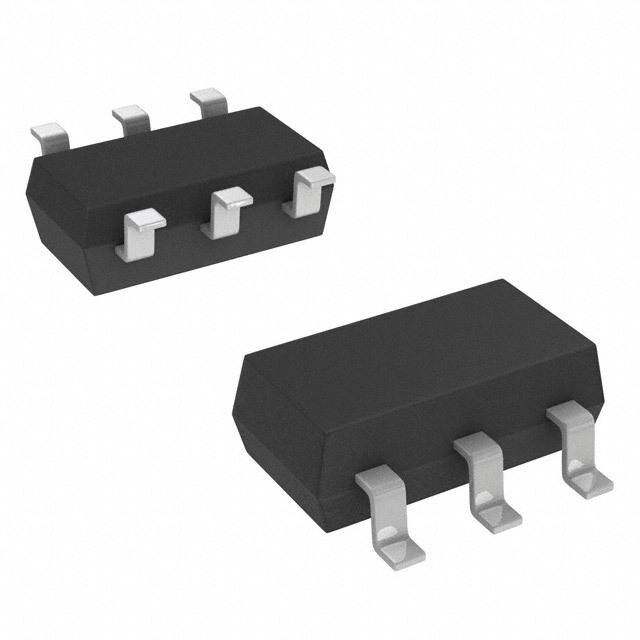
| 描述 | TVS DIODE 5.25VWM 17VC SOT23-6TVS二极管阵列 2 Line 2.5pF 10nA USB 2.0 Automotive |
| 产品分类 | |
| 品牌 | STMicroelectronics |
| 产品手册 | |
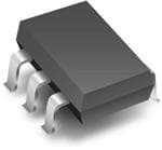
| 产品图片 |
|
| rohs | 符合RoHS无铅 / 符合限制有害物质指令(RoHS)规范要求 |
| 产品系列 | 二极管与整流器,TVS二极管,TVS二极管阵列,STMicroelectronics USBLC6-2SC6YUSB |
| 数据手册 | |
| 产品型号 | USBLC6-2SC6Y |
| 不同频率时的电容 | - |
| 产品培训模块 | http://www.digikey.cn/PTM/IndividualPTM.page?site=cn&lang=zhs&ptm=26067 |
| 产品种类 | TVS二极管阵列 |
| 供应商器件封装 | SOT-23-6 |
| 其它名称 | 497-11882-2 |
| 其它有关文件 | http://www.st.com/web/catalog/sense_power/FM114/CL1801/SC1494/PF251865?referrer=70071840 |
| 击穿电压 | 6 V |
| 功率-峰值脉冲 | - |
| 包装 | 带卷 (TR) |
| 单向通道 | - |
| 双向通道 | 2 |
| 商标 | STMicroelectronics |
| 外壳高度 | 1.45 mm |
| 安装类型 | 表面贴装 |
| 安装风格 | SMD/SMT |
| 封装 | Reel |
| 封装/外壳 | SOT-23-6 |
| 封装/箱体 | SOT-23-6L |
| 工作温度 | -40°C ~ 125°C (TJ) |
| 工作电压 | 1.1 V |
| 工厂包装数量 | 3000 |
| 应用 | 以太网 |
| 最大工作温度 | + 150 C |
| 最小工作温度 | - 40 C |
| 标准包装 | 3,000 |
| 电压-击穿(最小值) | 6V |
| 电压-反向关态(典型值) | 5.25V |
| 电压-箝位(最大值)@Ipp | 17V |
| 电容 | 2.5 pF |
| 电流-峰值脉冲(10/1000µs) | 5A (8/20µs) |
| 电源线路保护 | 是 |
| 端接类型 | SMD/SMT |
| 类型 | 转向装置(轨至轨) |
| 系列 | USBLC6-2SC6Y |
| 通道 | 2 Channels |
| 钳位电压 | 17 V |


PDF Datasheet 数据手册内容提取
USBLC6-2SC6Y Automotive very low capacitance ESD protection Datasheet production data Features ■ 2 data lines protected ■ Protects V BUS ■ Very low capacitance: 2.5 pF ■ Very low leakage current: 10 nA SOT23-6L USBLC6-2SC6Y(JEDEC MO178AB) ■ SOT23-6L package ■ RoHS compliant Figure 1. Functional diagram ■ AEC-Q101 qualified Benefits I/O1 11 6 I/O1 ■ Very low capacitance between lines to GND for optimized data integrity and speed GND 2 5 VBUS ■ Low PCB space consumption I/O2 3 4 I/O2 ■ Enhanced ESD protection. ISO10605 up to 25kV guaranteed at device level ■ ESD protection of V Applications BUS ■ High reliability offered by monolithic integration ■ USB 2.0 ports up to 480 Mb/s (high speed) ■ Fast response time ■ Compatible with USB 1.1 low and full speed ■ Consistent D+ / D- signal balance: ■ High-speed datalines in smart junction boxes – Very low capacitance matching tolerance ■ Ethernet port: 10/100 Mb/s I/O to GND = 0.015 pF ■ Video line protection – Compliant with USB 2.0 requirements Complies with the following standards Description ■ ISO10605: C = 150 pF, R = 330 The USBLC6-2SC6Y is a monolithic device – 25 kV (air discharge) dedicated to ESD protection of high speed – 15 kV (contact discharge) interfaces, such as USB 2.0, Ethernet links and video lines. ■ ISO10605: C = 330 pF, R = 330 – 15 kV (air discharge) The very low line capacitance secures a high level – 15 kV (contact discharge) of signal integrity without compromising in protecting sensitive chips against the most ■ ISO7637-3 stringent characterized ESD strikes. – Pulse 3a: Vs = -150 V – Pulse 3b: Vs = +100 V TM: Transil is a trademark of STMicroelectronics September 2012 Doc ID 023201 Rev 2 1/9 This is information on a product in full production. www.st.com 9
Characteristics USBLC6-2SC6Y 1 Characteristics T able 1. Absolute ratings Symbol Parameter Value Unit ISO 10605 (C = 150 pF, R = 330 ): Air discharge 25 Contact discharge 15 V (1) Peak pulse voltage kV PP ISO 10605 (C = 300 pF, R = 330 ): Air discharge 15 Contact discharge 15 T Storage temperature range -55 to +150 °C stg T Operating junction temperature range -40 to +150 °C j T Lead solder temperature (10 seconds duration) 260 °C L 1. For a surge greater than the maximum values, the diode will fail in short-circuit. Figure 2. Electrical characteristics (definitions) I IF Symbol Parameter V = Breakdown voltage BR IRM = Leakage current @VRM VF VIPRPM == SPetaankd p-ouflfs veo cltuargreent VCLVBR VRM IRM V CLINE= Line capacitance Slope:1/Rd IPP T able 2. Electrical characteristics (T = 25 °C) amb Symbol Parameter Test conditions Min. Typ. Max. Unit I Leakage current V = 5.25 V 10 150 nA RM RM Breakdown voltage between V V BUS I = 1 mA 6 V BR and GND R V Forward voltage I = 10 mA 1.1 V F F I = 1 A, 8/20 µs PP 12 V Any I/O pin to GND V Clamping voltage CL I = 5 A, 8/20 µs PP 17 V Any I/O pin to GND C Capacitance between I/O and GND 2.5 3.5 i/o-GND Interline capacitance matching VR = 1.65 V pF C 0.015 i/o-GND between I/O and GND C Capacitance between I/O 1.2 1.7 i/o-i/o Interline capacitance matching VR = 1.65 V pF C 0.04 i/o-i/o between I/O 2/9 Doc ID 023201 Rev 2
USBLC6-2SC6Y Characteristics F igure 3. Capacitance versus voltage Figure 4. Line capacitance versus frequency (typical values) (typical values) C(pF) C(pF) 3.0 2.8 2.6 CO= I/O - GND 2.4 2.5 2.2 VOSC= 30mVRMS F = 1MHz 2.0 Tj= 25°C 2.0 VOSC= 30mVRMS 1.8 VLINE= 0V to 3.3V Tj= 25°C 1.6 1.5 1.4 Cj= I/O - I/O 1.2 1.0 1.0 0.8 0.6 0.5 0.4 Data line voltage (V) 0.2 F(MHz) 0.0 0.0 0.0 0.5 1.0 1.5 2.0 2.5 3.0 3.5 4.0 4.5 5.0 1 10 100 1000 Figure 5. Relative variation of leakage Figure 6. Frequency response current versus junction temperature (typical values) IRM[Tj] /IRM[Tj=25°C] 0.00 100 S21(dB) VBUS=5V -5.00 -10.00 10 -15.00 Tj(°C) F(Hz) 1 -20.00 25 50 75 100 125 100.0k 1.0M 10.0M 100.0M 1.0G Figure 7. ESD response to ISO10605, Figure 8. ESD response to ISO10605, C=150pF, R = 330 (+15 kV air C=150pF, R=330(-15 kV air discharge) discharge) Vin Vin Vout Vout ESDSURGE ESDSURGE INTEST BOAORUDT INTEST BOAORUDT USBLC6-2SC6 +5V USBLC6-2SC6 +5V Doc ID 023201 Rev 2 3/9
Application and design guidelines USBLC6-2SC6Y Figure 9. Analog crosstalk results dB 0.00 -30.00 -60.00 -90.00 F (Hz) -120.00 100.0k 1.0M 10.0M 100.0M 1.0G 2 Application and design guidelines More information is available in the STMicroelectronics Application note AN2689, “Protection of automotive electronics from electrical hazards, guidelines for design and component selection”. 3 Ordering information scheme Figure 10. Ordering information scheme USB LC 6 - 2 SC6 Y Product designation Low capacitance Breakdown voltage 6 = 6.1V Number of lines protected 2 = 2 lines Package SC6 = SOT23-6L Automotive grade 4/9 Doc ID 023201 Rev 2
USBLC6-2SC6Y Package information 4 Package information ● Epoxy meets UL94, V0 ● Lead-free package In order to meet environmental requirements, ST offers these devices in different grades of ECOPACK® packages, depending on their level of environmental compliance. ECOPACK® specifications, grade definitions and product status are available at: www.st.com. ECOPACK® is an ST trademark. T able 3. SOT23-6L dimensions Dimensions Ref. Millimeters Inches Min. Typ. Max. Min. Typ. Max. A 0.90 1.45 0.035 0.057 c A1 θ L A1 0 0.15 0 0.006 A H E A2 0.90 1.30 0.035 0.051 b 0.30 0.50 0.012 0.020 c 0.09 0.20 0.004 0.008 e D 2.80 3.05 0.11 0.118 D b e E 1.50 1.75 0.059 0.069 e 0.95 0.037 A2 H 2.60 3.00 0.102 0.118 L 0.30 0.60 0.012 0.024 0° 10° 0° 10° F igure 11. SOT23-6L footprint 0.60 1.20 3.50 2.30 0.95 1.10 Doc ID 023201 Rev 2 5/9
Recommendation on PCB assembly USBLC6-2SC6Y 5 Recommendation on PCB assembly 5.1 Solder paste 1. Use halide-free flux, qualification ROL0 according to ANSI/J-STD-004. 2. “No clean” solder paste recommended. 3. Offers a high tack force to resist component displacement during PCB movement. 4. Use solder paste with fine particles: powder particle size 20-45 µm. 5.2 Placement 1. Manual positioning is not recommended. 2. It is recommended to use the lead recognition capabilities of the placement system, not the outline centering. 3. Standard tolerance of 0.05 mm is recommended. 4. 3.5 N placement force is recommended. Too much placement force can lead to squeezed out solder paste and cause solder joints to short. Too low placement force can lead to insufficient contact between package and solder paste that could cause open solder joints or badly centered packages. 5. To improve the package placement accuracy, a bottom side optical control should be performed with a high resolution tool. 6. For assembly, a perfect supporting of the PCB (all the more on flexible PCB) is recommended during solder paste printing, pick and place and reflow soldering by using optimized tools. 5.3 PCB design preference 1. To control the solder paste amount, the closed via is recommended instead of open vias. 2. The position of tracks and open vias in the solder area should be well balanced. The symmetrical layout is recommended, in case any tilt phenomena caused by asymmetrical solder paste amount due to the solder flow away. 6/9 Doc ID 023201 Rev 2
USBLC6-2SC6Y Recommendation on PCB assembly 5.4 Reflow profile Figure 12. ST ECOPACK® recommended soldering reflow profile for PCB mounting 240-245 °C Temperature (°C) -2°C/s 250 2 - 3 °C/s 200 60sec (90max) -3°C/s 150 -6°C/s 100 0.9 °C/s 50 Time (s) 0 30 60 90 120 150 180 210 240 270 300 Note: Minimize air convection currents in the reflow oven to avoid component movement. Doc ID 023201 Rev 2 7/9
Ordering information USBLC6-2SC6Y 6 Ordering information T able 4. Ordering information Order code Marking Package Weight Base qty Delivery mode USBLC6-2SC6Y UL2Y SOT23-6L 16.7 mg 3000 Tape and reel 7 Revision history T able 5. Document revision history Date Revision Changes 16-May-2012 1 First issue. 06-Sep-2012 2 Updated dimensions A max., b min. and L min. in Table3. 8/9 Doc ID 023201 Rev 2
USBLC6-2SC6Y Please Read Carefully: Information in this document is provided solely in connection with ST products. STMicroelectronics NV and its subsidiaries (“ST”) reserve the right to make changes, corrections, modifications or improvements, to this document, and the products and services described herein at any time, without notice. All ST products are sold pursuant to ST’s terms and conditions of sale. Purchasers are solely responsible for the choice, selection and use of the ST products and services described herein, and ST assumes no liability whatsoever relating to the choice, selection or use of the ST products and services described herein. No license, express or implied, by estoppel or otherwise, to any intellectual property rights is granted under this document. If any part of this document refers to any third party products or services it shall not be deemed a license grant by ST for the use of such third party products or services, or any intellectual property contained therein or considered as a warranty covering the use in any manner whatsoever of such third party products or services or any intellectual property contained therein. UNLESS OTHERWISE SET FORTH IN ST’S TERMS AND CONDITIONS OF SALE ST DISCLAIMS ANY EXPRESS OR IMPLIED WARRANTY WITH RESPECT TO THE USE AND/OR SALE OF ST PRODUCTS INCLUDING WITHOUT LIMITATION IMPLIED WARRANTIES OF MERCHANTABILITY, FITNESS FOR A PARTICULAR PURPOSE (AND THEIR EQUIVALENTS UNDER THE LAWS OF ANY JURISDICTION), OR INFRINGEMENT OF ANY PATENT, COPYRIGHT OR OTHER INTELLECTUAL PROPERTY RIGHT. UNLESS EXPRESSLY APPROVED IN WRITING BY TWO AUTHORIZED ST REPRESENTATIVES, ST PRODUCTS ARE NOT RECOMMENDED, AUTHORIZED OR WARRANTED FOR USE IN MILITARY, AIR CRAFT, SPACE, LIFE SAVING, OR LIFE SUSTAINING APPLICATIONS, NOR IN PRODUCTS OR SYSTEMS WHERE FAILURE OR MALFUNCTION MAY RESULT IN PERSONAL INJURY, DEATH, OR SEVERE PROPERTY OR ENVIRONMENTAL DAMAGE. ST PRODUCTS WHICH ARE NOT SPECIFIED AS "AUTOMOTIVE GRADE" MAY ONLY BE USED IN AUTOMOTIVE APPLICATIONS AT USER’S OWN RISK. Resale of ST products with provisions different from the statements and/or technical features set forth in this document shall immediately void any warranty granted by ST for the ST product or service described herein and shall not create or extend in any manner whatsoever, any liability of ST. ST and the ST logo are trademarks or registered trademarks of ST in various countries. Information in this document supersedes and replaces all information previously supplied. The ST logo is a registered trademark of STMicroelectronics. All other names are the property of their respective owners. © 2012 STMicroelectronics - All rights reserved STMicroelectronics group of companies Australia - Belgium - Brazil - Canada - China - Czech Republic - Finland - France - Germany - Hong Kong - India - Israel - Italy - Japan - Malaysia - Malta - Morocco - Philippines - Singapore - Spain - Sweden - Switzerland - United Kingdom - United States of America www.st.com Doc ID 023201 Rev 2 9/9