ICGOO在线商城 > UPA800T-T1-A
 Datasheet下载
- 型号: UPA800T-T1-A
- 制造商: CEL
- 库位|库存: xxxx|xxxx
- 要求:
| 数量阶梯 | 香港交货 | 国内含税 |
| +xxxx | $xxxx | ¥xxxx |
查看当月历史价格
查看今年历史价格
UPA800T-T1-A产品简介:
ICGOO电子元器件商城为您提供UPA800T-T1-A由CEL设计生产,在icgoo商城现货销售,并且可以通过原厂、代理商等渠道进行代购。 提供UPA800T-T1-A价格参考以及CELUPA800T-T1-A封装/规格参数等产品信息。 你可以下载UPA800T-T1-A参考资料、Datasheet数据手册功能说明书, 资料中有UPA800T-T1-A详细功能的应用电路图电压和使用方法及教程。
| 参数 | 数值 |
| 产品目录 | |
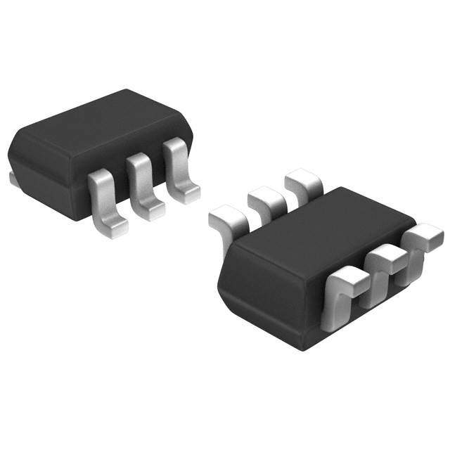
| 描述 | TRANSISTOR NPN HF FT=8GHZ SOT363 |
| 产品分类 | RF 晶体管 (BJT) |
| 品牌 | CEL |
| 数据手册 | |
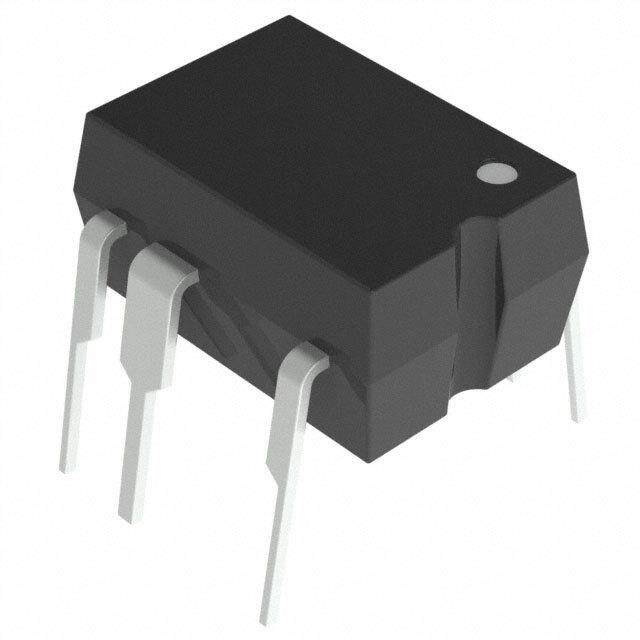
| 产品图片 |
|
| 产品型号 | UPA800T-T1-A |
| rohs | 无铅 / 符合限制有害物质指令(RoHS)规范要求 |
| 产品系列 | - |
| 不同 Ic、Vce 时的DC电流增益(hFE)(最小值) | 80 @ 5mA,3V |
| 产品目录页面 | |
| 供应商器件封装 | 6-SO |
| 其它名称 | UPA800T-ADKR |
| 功率-最大值 | 200mW |
| 包装 | Digi-Reel® |
| 噪声系数(dB,不同f时的典型值) | 1.9dB ~ 3.2dB @ 2GHz |
| 增益 | - |
| 安装类型 | 表面贴装 |
| 封装/外壳 | 6-TSSOP,SC-88,SOT-363 |
| 晶体管类型 | 2 NPN(双) |
| 标准包装 | 1 |
| 电压-集射极击穿(最大值) | 10V |
| 电流-集电极(Ic)(最大值) | 35mA |
| 频率-跃迁 | 8GHz |


- 商务部:美国ITC正式对集成电路等产品启动337调查
- 曝三星4nm工艺存在良率问题 高通将骁龙8 Gen1或转产台积电
- 太阳诱电将投资9.5亿元在常州建新厂生产MLCC 预计2023年完工
- 英特尔发布欧洲新工厂建设计划 深化IDM 2.0 战略
- 台积电先进制程称霸业界 有大客户加持明年业绩稳了
- 达到5530亿美元!SIA预计今年全球半导体销售额将创下新高
- 英特尔拟将自动驾驶子公司Mobileye上市 估值或超500亿美元
- 三星加码芯片和SET,合并消费电子和移动部门,撤换高东真等 CEO
- 三星电子宣布重大人事变动 还合并消费电子和移动部门
- 海关总署:前11个月进口集成电路产品价值2.52万亿元 增长14.8%

PDF Datasheet 数据手册内容提取
DATA SHEET SILICON TRANSISTOR m PA800T D HIGH-FREQUENCY LOW NOISE AMPLIFIER NPN SILICON EPITAXIAL TRANSISTOR (WITH BUILT-IN 2 ELEMENTS) MINI MOLD E The m PA800T has built-in 2 low-voltage transistors which are designed PACKAGE DRAWINGS U to amplify low noise in the VHF band to the UHF band. (Unit: mm) 2.1±0.1(cid:13) FEATURES 1.25±0.1(cid:13) • Low Noise N • NH|SiF2g1 h=e| 2G1 =.a9 6i nd.5B dTBY PT.Y @P. @f = f2 = G 2H Gz,H VzC, EV =CE 1 = V 1, IVC, =IC 3 = m 3A mA 2.0±0.2 1.3 0.650.65 12 XY 65 +0.10.2 –0 • A Mini Mold Package Adopted I 3 4 • Built-in 2 Transistors (2 · 2SC4228) T 1 ORDERING INFORMATION 0.9±0. 0.7 +0.15 –0 PART NUMBER QUANTITY PACKNING STYLE 0.1 0.1 ~ 0 mPA800T Loose products Embossed tape 8 mm wide. Pin 6 (Q1 (50 PCS) Base), Pin 5 (Q2 Base), Pin 4 (Q2 Emitter) PIN CONFIGURATION (Top View) face to perforation side of the tape. O mPA800T-T1 Taping products (3 KPCS/Reel) 6 5 4 Q1 Remark To order evaluation samples, please contact your nearby sales office. Q2 Part number for sample order: µPA800T-A (Unit Sample quantity is 50 pcs.) C 1 2 3 ABSOLUTE MAXIMUM RATINGS (TA = 25 (cid:176) C) PIN CONNECTIONS(cid:13)(cid:13) PARAMETER SYMBOL RATING UNIT 1. Collector (Q1)(cid:13) 4. Emitter (Q2)(cid:13) 2. Emitter (Q1)(cid:13) 5. Base (Q2)(cid:13) S 3. Collector (Q2) 6. Base (Q1)(cid:13) Collector to Base Voltage VCBO 20 V Collector to Emitter Voltage VCEO 10 V Emitter to Base Voltage VEBO 1.5 V I Collector Current IC 35 mA TDotal Power Dissipation PT 150 in 1 element mW 200 in 2 elementsNote Junction Temperature Tj 150 ˚C Storage Temperature Tstg –65 to +150 ˚C Note 110 mW must not be exceeded in 1 element. The information in this document is subject to change without notice. Document No. ID-3634 (O.D. No. ID-9141) Date Published April 1995 P
m PA800T ELECTRICAL CHARACTERISTICS (TA = 25 (cid:176) C) PARAMETER SYMBOL CONDITION MIN. TYP. MAX. UNIT Collector Cutoff Current ICBO VCB = 10 V, IE = 0 1.0 mA D Emitter Cutoff Current IEBO VEB = 1 V, IC = 0 1.0 mA DC Current Gain hFE VCE = 3 V, IC = 5 mANote 1 80 200 Gain Bandwidth Product fT VCE = 3 V, IC = 5 mA 5.5 80 GHz E Feed-back Capacitance Cre VCB = 3 V, IE = 0, f = 1 MHzNote 2 0.7 pF Insertion Power Gain (1) |S21e|2 VCE = 1 V, IC = 3 mA, f = 2 GHz 4.5 6.5 dB Insertion Power Gain (2) |S21e|2 VCE = 3 V, IC = 5 mA, f = 2 GHz 5.5 7.5 dB U Noise Figure (1) NF VCE = 1 V, IC = 3 mA, f = 2 GHz 1.9 3.2 dB Noise Figure (2) NF VCE = 3 V, IC = 5 mA, f = 2 GHz 1.9 3.2 dB Notes 1. Pulse Measurement: Pw £ 350 m s, Duty cycle £ 2 % N 2. Measured with 3-pin bridge, emitter and case should be connected to guard pin of bridge. hFE CLASSIFICATION Rank KB I Marking RL T hFE Value 80 to 200 TYPICAL CHARACTERISTICS (TA = 25 (cid:176) C) N PT - TA Characteristics IC - VCE Characteristics 25 W) Free OAir 160 m A m 200 20 P(T mA) 140 m A otal Power Dissipation 100 Per E2le EmleemnetCnts in Total Collector Current I(C 11505 IB =11 462802000000 mmmmmm AAAAAA T 0 S50 100 150 0 5 1.0 Ambient Temperature TA (°C) Collector to Emitter Voltage VCE (V) IIC - VBE Characteristics hFE - IC Characteristics 20 200 VCE = 3 V D VCE = 3 V 100 mA) hFE Current I (C 10 urrent Gain 50 ollector DC C 20 C 10 0 0.5 1.0 0.5 1 5 10 50 Base to Emitter Voltage VBE (V) Collector Current IC (mA) 2
m PA800T Cre - VCB Characteristics fT - IC Characteristics 5.0 10 F) f = 1 MHz Hz) fV =CE 2= G 3H Vz(cid:13) citance C (pre 12..00 Product f (GT 68 D pa h ck Ca 0.5 dwidt 4 E a n b a ed- 0.2 n B 2 Fe Gai 0.1 0 1 2 5 10 20 50 0.5 1 5 10 50 U Collector to Base Voltage VCB (V) Collector Current IC (mA) l S21e l 2 - IC Characteristics | S21e | 2 - f Characteristics N 12 25 2S | (dB)21e 8 Vf =CE 2= G3H Vz(cid:13) 2S | (dB) 21e 20 IVCC =E =5 3m VA(cid:13) Gain | Gain | I15 wer Twer 10 Po 4 Po Insertion N Insertion 5 0 0 0.5 1 5 10 50 0.1 0.5 1.0 2.0 5.0 Collector Current IC (mA) Frequency f (GHz) O NF - IC Characteristics 5 VCE = 3 V(cid:13) f = 2 GHz 4 B) C d e( 3 ur g Fi e 2 s oi N S 1 0 0.5 1 5 10 50 I Collector Current IC (mA) D 3
m PA800T S-PARAMETERS VCE = 3 V, IC = 5 mA, ZO = 50 W FREQUENCY S11 S21 S12 S22 D MHz MAG ANG MAG ANG MAG ANG MAG ANG 100.00 .875 –18.6 14.087 161.1 .018 78.2 .958 –10.1 200.00 .762 –35.0 12.290 145.1 .034 68.6 .888 –17.7 300.00 .677 –47.2 10.888 133.6 .048 66.6 .800 –24.4 400.00 .565 –59.4 9.275 123.6 .055 65.8 .719 –26.7 E 500.00 .495 –67.5 8.300 115.7 .063 63.5 .669 –28.7 600.00 .425 –76.1 7.184 108.9 .074 61.1 .610 –30.3 700.00 .372 –81.6 6.454 104.8 .084 63.8 .600 –30.6 800.00 .327 –88.5 5.818 99.5 .089 62.7 .560 –31.3 900.00 .289 –93.6 5.231 95.5 .092 64.6 .543 –30.1 1000.00 .255 –100.5 4.820 92.0 .104 62.8 U.519 –33.4 1100.00 .236 –105.2 4.444 88.8 .105 64.2 .512 –31.8 1200.00 .214 –112.2 4.142 85.3 .113 64.2 .497 –33.4 1300.00 .195 –117.6 3.842 83.2 .122 63.6 .476 –33.2 1400.00 .182 –123.8 3.554 79.3 .127 65.0 .481 –34.2 1500.00 .165 –129.9 3.343 77.4 .139 64.1 .467 –34.6 1600.00 .153 –137.4 3.218 75.3 .140 64.5 .466 –34.8 N 1700.00 .145 –144.3 3.091 73.6 .152 65.4 .458 –37.2 1800.00 .139 –151.8 2.857 70.4 .162 64.3 .456 –36.1 1900.00 .134 –157.0 2.764 68.7 .168 62.3 .451 –38.4 2000.00 .129 –164.7 2.624 66.4 .176 64.8 .445 –39.0 VCE = 3 V, IC = 3 mA, ZO = 50 W I FREQUENCY S11 S21 T S12 S22 MHz MAG ANG MAG ANG MAG ANG MAG ANG 100.00 .943 –13.4 9.384 165.9 .020 84.1 .969 –7.7 200.00 .868 –26.6 8.668 152.8 .038 77.2 .936 –13.8 300.00 .815 –37.7 8.165 142.9 .051 67.9 .876 –20.9 400.00 .717 –48.9 7.279 N132.9 .062 63.9 .804 –23.5 500.00 .655 –56.8 6.780 125.5 .075 63.9 .764 –26.7 600.00 .577 –65.5 6.061 118.0 .084 60.0 .708 –29.7 700.00 .518 –71.2 5.504 112.8 .091 59.7 .685 –31.1 800.00 .468 –78.1 5.074 106.7 .098 57.0 .639 –32.0 900.00 .420 –83.7 4.632 102.8 .102 59.0 .611 –32.8 1000.00 .380 –90.6 O4.340 98.3 .105 56.6 .592 –35.0 1100.00 .344 –94.8 3.951 94.8 .112 57.8 .579 –34.1 1200.00 .321 –101.6 3.717 90.5 .121 59.0 .551 –35.0 1300.00 .291 –105.9 3.485 87.6 .128 58.7 .532 –35.9 1400.00 .273 –111.7 3.306 84.3 .135 59.8 .535 –36.6 1500.00 .250 –117.2 3.134 80.7 .140 58.0 .511 –37.5 1600.00 .228 –122.4 2.959 79.0 .145 59.5 .516 –37.7 1700.00 .219 C–128.5 2.819 76.0 .153 59.0 .504 –39.0 1800.00 .199 –135.3 2.699 73.9 .161 58.4 .493 –39.9 1900.00 .193 –139.6 2.572 71.9 .163 60.3 .489 –41.4 2000.00 .182 –146.9 2.474 68.3 .175 59.8 .482 –41.4 VCE = 3 V, IC = 1 mA, ZO = 50 W S FREQUENCY S11 S21 S12 S22 MHz MAG ANG MAG ANG MAG ANG MAG ANG 100.00 1.023 –7.6 3.505 172.1 .025 86.4 .995 –4.6 200.00 .983 –16.1 3.400 163.3 .039 79.3 .986 –7.8 I 300.00 .975 –22.4 3.368 157.3 .061 74.6 .976 –12.8 400.00 .922 –31.8 3.219 149.1 .075 70.7 .936 –15.1 D500.00 .899 –36.9 3.186 143.3 .093 66.4 .922 –18.8 600.00 .849 –44.7 3.046 135.7 .105 62.2 .885 –22.5 700.00 .812 –50.6 2.905 131.1 .113 61.7 .880 –24.4 800.00 .774 –57.1 2.830 124.4 .128 55.7 .846 –27.2 900.00 .727 –62.9 2.694 119.2 .134 55.6 .808 –28.8 1000.00 .680 –69.3 2.597 114.1 .146 53.7 .790 –31.8 1100.00 .651 –74.1 2.479 109.3 .146 50.3 .766 –32.8 1200.00 .616 –79.8 2.392 104.8 .155 49.8 .741 –34.9 1300.00 .575 –85.2 2.302 101.1 .155 46.2 .714 –35.9 1400.00 .546 –90.6 2.207 96.0 .160 46.7 .708 –36.8 1500.00 .512 –95.8 2.110 92.1 .168 43.6 .685 –38.4 1600.00 .481 –100.6 2.034 88.8 .165 45.5 .676 –40.1 1700.00 .463 –106.3 1.989 85.5 .176 45.3 .667 –41.8 1800.00 .440 –111.8 1.903 82.2 .173 43.8 .649 –42.3 1900.00 .419 –116.4 1.854 78.9 .174 43.5 .633 –44.2 2000.00 .394 –121.2 1.779 75.5 .173 43.7 .630 –45.2 4
NOTICE 1. Descriptions of circuits, software and other related information in this document are provided only to illustrate the operation of semiconductor products and application examples. You are fully responsible for the incorporation of these circuits, software, and information in the design of your equipment. California Eastern Laboratories and Renesas Electronics assumes no responsibility for any losses incurred by you or third parties arising from the use of thDese circuits, software, or information. 2. California Eastern Laboratories has used reasonable care in preparing the information included in this document, but California Eastern Laboratories does not warrant that such information is error free. California Eastern Laboratories and Renesas Electronics assumes no liability whatsoever for any damages incurred by you resulting from errors in or omissions from the information included herein. 3. California Eastern Laboratories and Renesas Electronics do not assume any liability for infringement of patents, copyrights, or other intellectual property E rights of third parties by or arising from the use of Renesas Electronics products or technical information described in this document. No license, express, implied or otherwise, is granted hereby under any patents, copyrights or other intellectual property rights of California Eastern Laboratories or Renesas Electronics or others. 4. You should not alter, modify, copy, or otherwise misappropriate any Renesas Electronics product, whether in whole or in part. California Eastern Laboratories and Renesas Electronics assume no responsibility for any losses incurred by you or third parties arising from such alteration, modification, copy or otherwise misappropriation of Renesas Electronics product. U 5. Renesas Electronics products are classified according to the following two quality grades: “Standard” and “High Quality”. The recommended applications for each Renesas Electronics product depends on the product’s quality grade, as indicated below. “Standard”: Computers; office equipment; communications equipment; test and measurement equipment; audio and visual equipment; home electronic appliances; machine tools; personal electronic equipment; and industrial robots etc. “High Quality”: Transportation equipment (automobiles, trains, ships, etc.); traffic control systems; anti-disaster systems; anti-crime systems; and safety equipment etc. Renesas Electronics products are neither intended nor authorized foNr use in products or systems that may pose a direct threat to human life or bodily injury (artificial life support devices or systems, surgical implantations etc.), or may cause serious property damages (nuclear reactor control systems, military equipment etc.). You must check the quality grade of each Renesas Electronics product before using it in a particular application. You may not use any Renesas Electronics product for any application for which it is not intended. California Eastern Laboratories and Renesas Electronics shall not be in any way liable for any damages or losses incurred by you or third parties arising from the use of any Renesas Electronics product for which the product is not intended by California Eastern Laboratories or Renesas Electronics. 6. You should use the Renesas Electronics products described in this document within the rIange specified by California Eastern Laboratories, especially with respect to the maximum rating, operating supply voltage range, movement power voltage range, heat radiation characteristics, installation and other product characteristics. California Eastern Laboratories shall have no liability for malfunctiTons or damages arising out of the use of Renesas Electronics products beyond such specified ranges. 7. Although Renesas Electronics endeavors to improve the quality and reliability of its products, semiconductor products have specific characteristics such as the occurrence of failure at a certain rate and malfunctions under certain use conditions. Further, Renesas Electronics products are not subject to radiation resistance design. Please be sure to implement safety measures to guard them against the possibility of physical injury, and injury or damage caused by N fire in the event of the failure of a Renesas Electronics product, such as safety design for hardware and software including but not limited to redundancy, fire control and malfunction prevention, appropriate treatment for aging degradation or any other appropriate measures. Because the evaluation of microcomputer software alone is very difficult, please evaluate the safety of the final products or systems manufactured by you. 8. Please contact a California Eastern Laboratories sales office for details as to environmental matters such as the environmental compatibility of each Renesas Electronics product. Please use Renesas Electronics products in compliance with all applicable laws and regulations that regulate the inclusion or use of controlled substances, including without limitation, the EOU RoHS Directive. California Eastern Laboratories and Renesas Electronics assume no liability for damages or losses occurring as a result of your noncompliance with applicable laws and regulations. 9. Renesas Electronics products and technology may not be used for or incorporated into any products or systems whose manufacture, use, or sale is prohibited under any applicable domestic or foreign laws or regulations. You should not use Renesas Electronics products or technology described in this document for any purpose relating to military applications or use by the military, including but not limited to the development of weapons of mass destruction. When exporting the Renesas Electronics products or technology described in this document, you should comply with the applicable export control laws and regulations and follow the procedures requCired by such laws and regulations. 10. It is the responsibility of the buyer or distributor of California Eastern Laboratories, who distributes, disposes of, or otherwise places the Renesas Electronics product with a third party, to notify such third party in advance of the contents and conditions set forth in this document, California Eastern Laboratories and Renesas Electronics assume no responsibility for any losses incurred by you or third parties as a result of unauthorized use of Renesas Electronics products. 11. This document may not be reproduced or duplicated in any form, in whole or in part, without prior written consent of California Eastern Laboratories. 12. Please contact a California Eastern Laboratories sales office if you have any questions regarding the information contained in this document or Renesas S Electronics products, or if you have any other inquiries. NOTE 1: “Renesas Electronics” as used in this document means Renesas Electronics Corporation and also includes its majority-owned subsidiaries. NOTE 2: “Renesas Electronics product(s)” means any product developed or manufactured by or for Renesas Electronics. NOTE 3: Products and product information are subject to change without notice. I D CEL Headquarters • 4590 Patrick Henry Drive, Santa Clara, CA 95054 • Phone (408) 919-2500 • www.cel.com For a complete list of sales offices, representatives and distributors, Please visit our website: www.cel.com/contactus