ICGOO在线商城 > 集成电路(IC) > PMIC - 电源管理 - 专用 > MAX16128UAACAC+

 Datasheet下载
- 型号: MAX16128UAACAC+
- 制造商: Maxim
- 库位|库存: xxxx|xxxx
- 要求:
| 数量阶梯 | 香港交货 | 国内含税 |
| +xxxx | $xxxx | ¥xxxx |
查看当月历史价格
查看今年历史价格
MAX16128UAACAC+产品简介:
ICGOO电子元器件商城为您提供MAX16128UAACAC+由Maxim设计生产,在icgoo商城现货销售,并且可以通过原厂、代理商等渠道进行代购。 MAX16128UAACAC+价格参考。MaximMAX16128UAACAC+封装/规格:PMIC - 电源管理 - 专用, Load Dump, Voltage Protection PMIC 8-uMAX。您可以下载MAX16128UAACAC+参考资料、Datasheet数据手册功能说明书,资料中有MAX16128UAACAC+ 详细功能的应用电路图电压和使用方法及教程。
Maxim Integrated的MAX16128UAACAC+是一款专用电源管理IC(PMIC),主要面向需要高精度电源监控和管理的应用场景。该器件具备多通道电压监测、看门狗定时器、手动复位输入以及电源故障比较器等功能,适用于对系统稳定性与可靠性要求较高的工业、通信及汽车电子等领域。

典型应用场景包括:

1. 工业控制系统:用于PLC、工业计算机及自动化设备中,确保系统在电源异常时能够及时复位或采取保护措施,防止数据丢失或设备损坏。

2. 通信设备:如基站、路由器和交换机等,用于监测关键电源电压,提供系统复位信号,保障通信系统的稳定运行。

3. 汽车电子系统:用于车载控制模块(如ECU),监控车辆电源状态,确保在电压异常时系统能可靠复位。

4. 医疗设备:用于对电源稳定性和系统可靠性要求严格的医疗仪器中,提供精准的电压监控与复位功能。

该器件采用TQFN封装,支持宽工作温度范围,具备较高的集成度和灵活性,适合需要多电源监控和系统复位管理的复杂应用。
| 参数 | 数值 |
| 产品目录 | 集成电路 (IC) |
| 描述 | IC LOAD DUMP REV V PROT 8UMAX |
| 产品分类 | |
| 品牌 | Maxim Integrated |
| 数据手册 | |
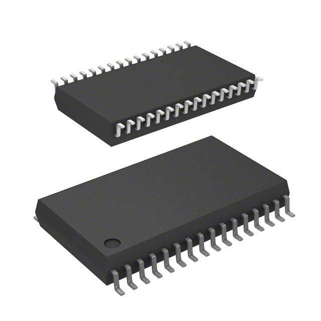
| 产品图片 |
|
| 产品型号 | MAX16128UAACAC+ |
| rohs | 无铅 / 符合限制有害物质指令(RoHS)规范要求 |
| 产品系列 | - |
| 供应商器件封装 | 8-uMAX |
| 包装 | 管件 |
| 安装类型 | 表面贴装 |
| 封装/外壳 | 8-TSSOP,8-MSOP(0.118",3.00mm 宽) |
| 工作温度 | -40°C ~ 125°C |
| 应用 | 负载突降,电压保护 |
| 标准包装 | 1 |
| 电压-电源 | 3 V ~ 30 V |
| 电流-电源 | 260µA |


PDF Datasheet 数据手册内容提取
Click here for production status of specific part numbers. MAX16128/MAX16129 Load-Dump/Reverse-Voltage Protection Circuits General Description Benefits and Features The MAX16128/MAX16129 load-dump/reverse-voltage ● Increases Protection of Sensitive Electronic protection circuits protect power supplies from damaging Components in Harsh Environments input-voltage conditions, including overvoltage, reverse- • -36V to +90V Wide Input-Voltage Protection Range voltage, and high-voltage transient pulses. Using a • Fast Gate Shutoff During Fault Conditions with built-in charge pump, the devices control two external Complete Load Isolation back-to-back n-channel MOSFETs that turn off and isolate • Thermal Shutdown Protection downstream power supplies during damaging input • FLAG Output Identifies Fault Condition conditions, such as an automotive load-dump pulse or a ● Automotive Qualified reverse-battery condition. Operation is guaranteed down • Operates Down to +3V, Riding Out Cold-Crank to 3V that ensures proper operation during automotive Conditions cold-crank conditions. These devices feature a flag output • -40°C to +125°C Operating Temperature Range (FLAG) that asserts during fault conditions. ● Integration Reduces Solution Size For reverse-voltage protection, external back-to-back • Internal Charge-Pump Circuit Enhances External MOSFETs outperform the traditional reverse-battery n-Channel MOSFET diode, minimizing the voltage drop and power dissipation • Fixed Undervoltage/Overvoltage Thresholds during normal operation. • 3mm × 3mm, 8-Pin µMAX Package The devices use fixed overvoltage and undervoltage ● Reduced Power Dissipation Compared to Discrete thresholds, minimizing the external component count. Solutions The MAX16129 provides limiter-mode fault management • Minimal Operating Voltage Drop for Reverse- for overvoltage and thermal-shutdown conditions; whereas Voltage Protection the MAX16128 provides switch-mode fault management • 380µA Supply Current and 100µA Shutdown for overvoltage and thermal shutdown conditions. In the Current at 30V Input limiter mode, the output voltage is limited and FLAG is asserted low during a fault. In the switch mode, the external MOSFETs are switched off and FLAG is asserted low after a fault. The switch mode is available in four Ordering Information appears at end of data sheet. options—Latch mode, 1 Autoretry mode, 3 Autoretry mode, and Always autoretry mode. The MAX16128/MAX16129 are available in an 8-pin µMAX® package and operate over the automotive temperature range (-40°C to +125°C). Applications ● Automotive ● Industrial ● Avionics ● Telecom/Server/Networking µMAX is a registered trademark of Maxim Integrated Products, Inc. 19-6146; Rev 6; 8/19
MAX16128/MAX16129 Load-Dump/Reverse-Voltage Protection Circuits Absolute Maximum Ratings (All pins referenced to GND.) Continuous Power Dissipation (TA = +70°C) (multilayer board) IN ............................................................................-36V to +90V µMAX (derate 12.9mW/°C above +70°C) ..............1030.9mW SHDN ...........................................-0.3V to max (0V, VIN + 0.3V) Operating Temperature Range .........................-40°C to +125°C SRC, GATE ............................................................-36V to +45V Junction Temperature ......................................................+150°C SRC to GATE .........................................................-36V to +30V Storage Temperature Range ............................-60°C to +150°C OUT .......................................................................-0.3V to +45V Lead Temperature (soldering, 10s) .................................+300°C FLAG .....................................................................-0.3V to +45V Soldering Temperature (reflow) .......................................+260°C Continuous Sink/Source (All Pins) .................................±100mA Stresses beyond those listed under “Absolute Maximum Ratings” may cause permanent damage to the device. These are stress ratings only, and functional operation of the device at these or any other conditions beyond those indicated in the operational sections of the specifications is not implied. Exposure to absolute maximum rating conditions for extended periods may affect device reliability. Package Thermal Characteristics (Note 1) µMAX Junction-to-Ambient Thermal Resistance (θJA) .......77.6°C/W Junction-to-Case Thermal Resistance (θJC) .................5°C/W Note 1: Package thermal resistances were obtained using the method described in JEDEC specification JESD51-7, using a four-layer board. For detailed information on package thermal considerations, refer to www.maximintegrated.com/thermal-tutorial. Electrical Characteristics (VIN = 12V, CGATE-SOURCE = 1nF, TA = -40°C to +125°C, unless otherwise noted. Typical values are at TA = +25°C.) (Note 2) PARAMETER SYMBOL CONDITIONS MIN TYP MAX UNITS Operating range 3 30 Input Voltage Range VIN V Protection range -36 +90 VIN = VSRC = VOUT 260 360 = 12V SHDN = high Input Supply Current IIN =V I3N0 =V VSRC = VOUT 290 400 µA VIN = 12V 44 60 SHDN = low VIN = 30V 64 100 VIN = VSRC = 12V, SHDN = high 36 200 SRC Input Current ISRC µA VIN = VSRC = 30V, SHDN = high 240 350 0.97 × 1.03 × Internal Undervoltage Threshold VUV_TH VIN rising VUV VUV VUV V Internal Undervoltage-Threshold 0.05 × Hysteresis VUV_HYS VUV V 0.97 × 1.03 × Internal Overvoltage Threshold VOV_TH VIN rising VOV VOV VOV V Internal Overvoltage-Threshold 0.05 × Hysteresis VOV_HYS VOV V www.maximintegrated.com Maxim Integrated │ 2
MAX16128/MAX16129 Load-Dump/Reverse-Voltage Protection Circuits Electrical Characteristics (continued) (VIN = 12V, CGATE-SOURCE = 1nF, TA = -40°C to +125°C, unless otherwise noted. Typical values are at TA = +25°C.) (Note 2) PARAMETER SYMBOL CONDITIONS MIN TYP MAX UNITS 0.97 × 1.03 × Internal Cold-Crank Threshold VCCK VIN falling VCCK VCCK VCCK V 0.05 × Internal Cold-Crank Threshold Hysteresis VCCK_HYS VCCK V MAX16128 4 OUT Input Resistance to Ground ROUT MW MAX16129 2 POK Threshold Rising VPOK+ 0.9 x VIN V 0.87 × POK Threshold Falling VPOK- VIN V Startup Response Time tSTART (Note 3) 150 µs Autoretry Timeout tRETRY 150 ms GATE Rise Time tRISE VGATE rising (GND to VSRC + 8V) 1 ms VIN rising (MAX16128) from Overvoltage-to-GATE Propagation Delay tOVG V(0O.9U T× rVisOinVg_ T(MH)A tXo 1(16.112 ×9 )V frOoVm_TH), 1 µs (0.9 × VOV_TH) to (1.1 × VOV_TH) Undervoltage-to-GATE Propagation Delay tUVG V(0I.N9 f×a lVlinUgV f_rToHm) (1.1 × VUV_TH) to 21 µs VIN rising (MAX16128) from Overvoltage to FLAG Propagation Delay tOV V(0O.9U T× rVisOinVg_ T(MH)A tXo 1(16.112 ×9 )V frOoVm_TH) 1 µs (0.9 × VOV_TH) to (1.1 × VOV_TH) VIN = VSRC = VOUT = 3V, 4.25 5 5.5 IGATE = -1µA VIN = VSRC = VOUT = 12V, 8 9 10 IGATE = -1µA GATE Output Voltage High Above VSRC VGS V VIN = VSRC = VOUT = 24V, 7 8.5 10 IGATE = -1µA VIN = VSRC = VOUT = 30V, 6.25 8 9.5 IGATE = -1µA GATE Pulldown Current IPD VGATE = 12V 8.8 mA GATE Charge-Pump Current IGATE VIN = VGATE = VSRC = 12V 180 µA Thermal Shutdown T+ +145 °C Thermal-Shutdown Hysteresis ∆T 15 °C SHDN Logic-High Input Voltage VIH 1.4 V SHDN Logic-Low Input Voltage VIL 0.4 V www.maximintegrated.com Maxim Integrated │ 3
MAX16128/MAX16129 Load-Dump/Reverse-Voltage Protection Circuits Electrical Characteristics (continued) (VIN = 12V, CGATE-SOURCE = 1nF, TA = -40°C to +125°C, unless otherwise noted. Typical values are at TA = +25°C.) (Note 2) PARAMETER SYMBOL CONDITIONS MIN TYP MAX UNITS SHDN Input Pulse Width tPW 6 µs SHDN Input Pulldown Current ISPD 0.8 1.2 µA FLAG Output Voltage Low VOL FLAG sinking 1mA 0.4 V FLAG Leakage Current IIL VFLAG = 12V 0.5 µA Note 2: All parameters are production tested at TA = +25°C. Limits over the operating temperature range are guaranteed by design and characterization. Note 3: The MAX16128/MAX16129 power up with the external MOSFETs in off mode (VGATE = VSRC). The external MOSFETs turn on tSTART after the devices are powered up and all input conditions are valid. Typical Operating Characteristics (VIN = 12V, TA = +25°C, unless otherwise noted.) SUPPLY CURRENT SUPPLY CURRENT SHUTDOWN SUPPLY CURENT vs. SUPPLY VOLTAGE vs. TEMPERATURE vs. SUPPLY VOLTAGE A)µ 235000 SGHADTEN E=N HHIGAHNCED MAX16128/29 toc01 µA) 223791000 SGHADTEN E=N HHIGAHNCED MAX16128/29 toc02 A)µ 1089000 SHDN = LOW MAX16128/29 toc03 T ( T ( T ( 70 N N 250 N E 200 E E R R R 60 R R R U U 230 U PLY C 150 PLY C 210 PLY C 50 P P P 40 U U U S S 190 S 100 30 170 20 50 150 10 3 13 23 33 -40 -20 0 20 40 60 80 100 120 3 9 15 21 27 SUPPLY VOLTAGE (V) TEMPERATURE (°C) SUPPLY VOLTAGE (V) SHUTDOWN SUPPLY CURRENT SHDN PULLDOWN CURRENT vs. TEMPERATURE vs. TEMPERATURE µRRENT (A) 34455050 SHDN = LOW MAX16128/29 toc04 µN CURRENT (A) 00001.....67890 MAX16128/29 toc05 U 30 W 0.5 PLY C 25 LLDO 0.4 P U U P 0.3 S 20 N HD 0.2 S 15 0.1 10 0 -40 -25 -10 5 20 35 50 65 80 95 110125 -40 -25 -10 5 20 35 50 65 80 95 110125 TEMPERATURE (°C) TEMPERATURE (°C) www.maximintegrated.com Maxim Integrated │ 4
MAX16128/MAX16129 Load-Dump/Reverse-Voltage Protection Circuits Typical Operating Characteristics (continued) (VIN = 12V, TA = +25°C, unless otherwise noted.) GATE-TO-SRC VOLTAGE GATE PULLDOWN CURRENT GATE-TO-SRC VOLTAGE vs. VIN vs. TEMPERATURE vs. TEMPERATURE E (V) 1890 MAX16128/29 toc06 E (V)1099...026 MAX16128/29 toc07 NT (mA) 1207 VGATE = 12V MAX16128/29 toc08 G 7 G 8.8 E A A R T T R RC VOL 56 RC VOL 88..04 WN CU 14 S S O ATE-TO- 34 ATE-TO- 77..26 E PULLD 11 G 2 G 6.8 AT 8 G 1 6.4 VIN = VSRC = VOUT = 12V GATE ENHANCED 0 6.0 5 0 5 10 15 20 25 30 35 -40 -25 -10 5 20 35 50 65 80 95 110125 -40 -25 -10 5 20 35 50 65 80 95 110125 VIN (V) TEMPERATURE (°C) TEMPERATURE (°C) INTERNAL OVERVOLTAGE THRESHOLD GATE PULLUP CURRENT vs. VIN vs. TEMPERATURE µENT (A) 111246800000 MAX16128/29 toc09 RESHOLD (%V)OV11009208 RISING MAX16128/29 toc10A RR 120 TH CU E LL-UP 10800 OLTAG 96 PU 60 RV 94 ATE 40 OVE FALLING G AL 92 20 VIN = VGATE = VSRC RN GATE ENHANCED E T 0 N 90 I 0 5 10 15 20 25 30 -40 -25 -10 5 20 35 50 65 80 95 110125 VIN (V) TEMPERATURE (°C) INTERNAL UNDERVOLTAGE THRESHOLD FLAG OUTPUT LOW VOLTAGE vs. TEMPERATURE vs. CURRENT )V HRESHOLD (%VU111000240 MAX16128/29 toc10B E (V) 00..45 MAX16128/29 toc11 E T AG 0.3 ERVOLTAG 9968 RISING FLAG VOLT 0.2 ND 94 NAL U 92 FALLING 0.1 R E T N 90 0 I -40 -25 -10 5 20 35 50 65 80 95 110125 0 0.5 1.0 1.5 2.0 TEMPERATURE (°C) FLAG CURRENT (mA) www.maximintegrated.com Maxim Integrated │ 5
MAX16128/MAX16129 Load-Dump/Reverse-Voltage Protection Circuits Typical Operating Characteristics (continued) (VIN = 12V, TA = +25°C, unless otherwise noted.) OVERVOLTAGE FAULT-TO-GATE REVERSE CURRENT PROPAGATION DELAY vs. TEMPERATURE vs. REVERSE VOLTAGE µLAY (s) 21..80 MAX16128/29 toc12 µNT (A) 223050 MAX16128/29 toc13 DE 1.6 RE PROPAGATION 1.4 REVERSE CUR 1105 1.2 5 1.0 0 -40 -25 -10 5 20 35 50 65 80 95 110125 0 5 10 15 20 25 30 TEMPERATURE (°C) REVERSE VOLTAGE (V) STARTUP WAVEFORM STARTUP FROM SHUTDOWN (SHDN) (VIN PULSED O TO 12V, RLOAD = 100Ω, RISING FROM O TO 2V, VIN = 12V, CIN = 0.1µF, COUT = 10µF) RLOAD = 100Ω, CIN = 0.1µF MAX16128/29 toc14 MAX16128/29 toc15 VIN VSHDN 10V/div 2V/div VGATE VGATE 10V/div 10V/div VOUT VOUT 10V/div 10V/div 200µs/div 400µs/div OVERVOLTAGE SWITCH FAULT OVERVOLTAGE LIMITER (VOV = 21V, CIN = 0.1µF, COUT = 10µF) (VOV = 21V, CIN = 0.1µF, COUT = 10µF) MAX16128/29 toc16 MAX16128/29 toc17 VIN 20V/div VIN 20V/div VGATE 20V/div VGATE VOUT 10V/div 10V/div VOUT 10V/div 20ms/div 20ms/div www.maximintegrated.com Maxim Integrated │ 6
MAX16128/MAX16129 Load-Dump/Reverse-Voltage Protection Circuits Pin Configuration TOP VIEW + OUT 1 8 FLAG SRC 2 MAX16128 7 I.C. MAX16129 GATE 3 6 GND IN 4 5 SHDN µMAX Pin Description PIN NAME FUNCTION Output Voltage-Sense Input. Connect OUT to the load with a 100W series resistor. Bypass with a minimum 1 OUT 10µF capacitor to GND. Source Input. Connect SRC to the common source connection of the external MOSFETs. When the 2 SRC MOSFETs are turned off, this connection is clamped to GND. An external zener diode between SRC and GATE protects the gates of the external MOSFETs. Gate-Driver Output. Connect GATE to the gates of the external n-channel MOSFETs. GATE is the charge- 3 GATE pump output during normal operation. GATE is quickly pulled low during a fault condition or when SHDN is pulled low. Positive Supply Input Voltage. Connect IN to the positive side of the input voltage. Bypass IN with a 0.1µF 4 IN ceramic capacitor to GND. Shutdown Input. Drive SHDN low to force GATE and FLAG low and turn off the external n-channel 5 SHDN MOSFETs. Connect a 100kW resistor from SHDN to IN for normal operation. 6 GND Ground 7 I.C. Internally connected to GND FLAG Output. During startup, FLAG is low as long as VOUT is lower than 90% of VIN and after that it is high impedance. It asserts low during shutdown mode, an overvoltage, thermal shutdown, or 8 FLAG undervoltage fault or when VOUT falls below 90% of VIN. FLAG asserts low during a cold-crank fault to signal reverse-current protection. www.maximintegrated.com Maxim Integrated │ 7
MAX16128/MAX16129 Load-Dump/Reverse-Voltage Protection Circuits Detailed Description Overvoltage Limiter (MAX16129) The MAX16128/MAX16129 transient protection circuits In overvoltage-limiter mode, the output voltage is regu- are suitable for automotive and industrial applications lated at the overvoltage-threshold voltage and continues where high-voltage transients are commonly present on to supply power to downstream devices. In this mode, the supply voltage inputs. The devices monitor the input volt- device operates like a voltage regulator. age and control two external common-source n-channel During normal operation, GATE is enhanced 9V above MOSFETs to protect downstream voltage regulators dur- SRC. The output voltage is monitored through an internal ing load-dump events or other automotive pulse condi- resistive divider. When OUT rises above the overvoltage tions. threshold, GATE goes low and the MOSFETs turn off. As The devices feature an overvoltage and an undervoltage the voltage on OUT falls below the overvoltage threshold comparator for voltage window detection. A flag output minus the threshold hysteresis, GATE goes high and (FLAG) asserts when a fault event occurs. the MOSFETs turn back on again, regulating OUT in a switched-linear mode at the overvoltage threshold. Two external back-to-back n-channel MOSFETs provide reverse-voltage protection and also prevent reverse The switching frequency depends on the gate charge of current during a fault condition. Compared to a traditional the MOSFETs, the charge-pump current, the output load reverse-battery diode, this approach minimizes power dis- current, and the output capacitance. sipation and voltage drop. Caution must be exercised when operating the The MAX16129 provides a limiter-mode fault manage- MAX16129 in voltage-limiting mode for long durations. ment for overvoltage and thermal-shutdown conditions, Since MOSFETs can dissipate power continuously during whereas the MAX16128 provides switch-mode fault this interval, proper heatsinking should be implemented to management for overvoltage and thermal-shutdown con- prevent damage to them. ditions. In the limiter mode, the MOSFETs cycle on and Overvoltage Switch (MAX16128) off so the output voltage is limited. In the switch mode, In the overvoltage switch mode, the internal overvolt- the external MOSFETs are switched off, disconnecting age comparator monitors the input voltage and the load the load from the input. In both cases, FLAG asserts to is completely disconnected from the input during an indicate a fault. overvoltage event. When the input voltage exceeds the Gate Charge Pump overvoltage threshold, GATE goes low and the MOSFETs The devices use a charge pump to generate the GATE to turn off, disconnecting the input from the load. After that, SRC voltage and enhance the external MOSFETs. After for the autoretry-mode version, the autoretry timer starts, the input voltage exceeds the input undervoltage thresh- while for the latched-mode version a power cycle to IN or old, the charge pump turns on after a 150µs delay. a cycle on SHDN is needed to turn the external MOSFETs back on. During a fault condition, GATE is pulled to ground with an 8.8mA (min) pulldown current. Note that an exter- The MAX16128 can be configured to latch off (suffix D) nal zener diode is required to be connected between even after the overvoltage condition ends. The latch is the gate and source of the external MOSFETs (see the cleared by cycling IN below the undervoltage threshold or Applications Information section). by toggling SHDN. The devices can also be configured to retry: Overvoltage Protection ● One time, then latch off (suffix B) The devices detect overvoltage conditions using a com- parator that is connected through an internal resistive ● Three times, then latch off (suffix C) divider to the input or output voltage. An overvoltage ● Always retry and never latch off (suffix A) condition causes the GATE output to go low, turning off There is a fixed 150ms (typ) delay between each retry the external MOSFETs. FLAG also asserts to indicate the attempt. If the overvoltage-fault condition is gone when fault condition. a retry is attempted, GATE goes high and power is restored to the downstream circuitry. www.maximintegrated.com Maxim Integrated │ 8
MAX16128/MAX16129 Load-Dump/Reverse-Voltage Protection Circuits Undervoltage Protection absolute maximum junction-temperature rating of TJ = +150°C. The devices monitor the input voltage for undervoltage conditions. If the input voltage is below the undervoltage Flag Output (FLAG) threshold (VIN < VUV_TH - VUV_HYS), GATE goes low, An open-drain FLAG output indicates fault conditions. turning off the external MOSFETs and FLAG asserts. During startup, FLAG is initially low and goes high imped- When the input voltage exceeds the undervoltage threshold (VIN > VUV_TH), GATE goes high after a 150µs delay ance when VOUT is greater than 90% of VIN if no fault conditions are present. FLAG asserts low during shut- (typ). down mode, an overvoltage, thermal shutdown, or under- For the MAX16128/MAX16129, the undervoltage threshold voltage fault, or when VOUT falls below 90% of VIN. In is determined by the part number suffix option (see Table 2). the versions where the cold-crank comparator is enabled, FLAG asserts low during a cold-crank fault. Cold-Crank Monitoring Cold-crank faults occur when the input voltage decreases Reverse-Voltage Protection from its steady-state condition. A cold-crank compara- The devices integrate reverse-voltage protection, pre- tor monitors IN through an internal resistive divider. The venting damage to the downstream circuitry caused by MAX16128/MAX16129 offer two ways to handle this battery reversal or negative transients. The devices can kind of fault depending on a part number suffix (see the withstand reverse voltage to -36V without damage to Selector Guide): themselves or the load. During a reverse-voltage condi- ● The cold-crank comparator is disabled and external tion, the two external n-channel MOSFETs are turned off, MOSFETs stay on during the falling input-voltage protecting the load. Connect a 0.1µF ceramic capacitor transient unless the input voltage falls below the un- from IN to GND connect a 10µF capacitor from OUT to dervoltage threshold (see Table 2). GND, and minimize the parasitic capacitance from GATE to GND to have fast reverse-battery voltage-transient ● The cold-crank comparator is enabled and external protection. During normal operation, both MOSFETs are MOSFETs are switched off by pulling down GATE if turned on and have a minimal forward-voltage drop, pro- the input voltage falls below the cold-crank threshold viding lower power dissipation and a much lower voltage to avoid load discharge due to reverse current from drop than a reverse-battery protection diode. OUT to IN (see Table 4). In the last case, cold-crank protection is enabled as long Applications Information as VOUT is higher than 90% of VIN (with a 3% hysteresis) Automotive Electrical Transients and VIN is higher than the undervoltage threshold. When (Load Dump) the monitored input voltage falls below the falling cold- crank fault threshold (VIN < VCCK), the GATE is pulled ● Automotive circuits generally require supply voltage down and FLAG is asserted low. When the input voltage protection from various transient conditions that occur rises back above the rising cold-crank fault threshold in automotive systems. Several standards define various (VIN > VCCK + VCLK_HYS), FLAG is released and the pulses that can occur. Table 1 summarizes the pulses charge pump enhances GATE above SRC, reconnecting from the ISO 7637-2 and ISO 16750-2 specification. the load to the input. Most of the pulses can be mitigated with capacitors and zener clamp diodes (see the Typical Operating Thermal Shutdown Characteristics and also the Increasing the Operating The devices’ thermal-shutdown feature turns off the Voltage Range section). The load dump (pulse 5a and MOSFETs if the internal die temperature exceeds 145°C 5b) occurs when the alternator is charging the battery (TJ). By ensuring good thermal coupling between the and a battery terminal gets disconnected. Due to the sudden MOSFETs and the devices, the thermal shutdown can change in load, the alternator goes out of regulation turn off the MOSFETs if they overheat. and the bus voltage spikes. The pulse has a rise time When the junction temperature exceeds TJ = +145°C of about 10ms and a fall time of about 400ms but can (typ), the internal thermal sensor signals the shutdown extend out to 1s or more depending on the characteris- logic, pulling the GATE voltage low and allowing the tics of the charging system. The magnitude of the pulse device to cool. When TJ drops by 15°C (typ), GATE goes depends on the bus voltage and whether the system is high and the MOSFETs turn back on. Do not exceed the unsuppressed or uses central load-dump suppression www.maximintegrated.com Maxim Integrated │ 9
MAX16128/MAX16129 Load-Dump/Reverse-Voltage Protection Circuits Table 1. Summary of ISO 7637-2 Pulses and ISO 16750-2 PEAK VOLTAGE (V) (MAX)* NAME DESCRIPTION DURATION 12V SYSTEM Pulse 1 Inductive load disconnection -100 1 to 2ms Pulse 2a Inductive wiring disconnection 50 0.05ms Pulse 3a -150 Switching transients 0.2µs Pulse 3b 100 -7 100ms (initial) Pulse 4 Cold crank -6 Up to 20s Pulse 5a Load dump (unsuppressed) 87 400ms (single) Pulse 5b Load dump (suppressed) (Varies, but less than pulse 5a) *Relative to system voltage. (generally implemented using very large clamp diodes and turn-off time. MOSFETs with more gate capacitance built into the alternator). Table 1 lists the worst-case tend to respond more slowly. values from the ISO 7637-2 specification. MOSFET Power Dissipation Cold crank (pulse 4) occurs when activating the starter The RDS(ON) must be low enough to limit the MOSFET motor in cold weather with a marginal battery. Due to the power dissipation during normal operation. Power large load imposed by the starter motor, the bus voltage dissipation (per MOSFET) during normal operation can be sags. Since the devices can operate down to 3V, the calculated using this formula: downstream circuitry can continue to operate through a cold-crank condition. If desired, the undervoltage thresh- P = ILOAD2 × RDS(ON) old can be increased so that the MOSFETs turn off during where P is the power dissipated in each MOSFET and a cold crank, disconnecting the downstream circuitry. An ILOAD is the average load current. output reservoir capacitor can be connected from OUT to During a fault condition in switch mode, the MOSFETs GND to provide energy to the circuit during the cold-crank turn off and do not dissipate power. Limiter mode imposes condition. the worst-case power dissipation. The average power can Refer to the ISO 7637-2 specification for details on pulse be computed using the following formula: waveforms, test conditions, and test fixtures. P = ILOAD × (VIN - VOUT) MOSFET Selection where P is the average power dissipated in both MOSFETs, MOSFET selection is critical to design a proper protec- ILOAD is the average load current, VIN is the input volt- tion circuit. Several factors must be taken into account: age, and VOUT is the average limited voltage on the the gate capacitance, the drain-to-source voltage rating, output. In limiter mode, the output voltage is a sawtooth the on-resistance (RDS(ON)), the peak power-dissipation wave with characteristics determined by the RDS(ON) of capability, and the average power-dissipation limit. In gen- the MOSFETs, the output load current, the output capaci- eral, both MOSFETs should have the same part number. tance, the gate charge of the MOSFETs, and the GATE For size-constrained applications, a dual MOSFET can charge-pump current. save board area. Select the drain-to-source voltage so Since limiter mode can involve high switching currents that the MOSFETs can handle the highest voltage that when the GATE is turning on at the start of a limiting might be applied to the circuit. Gate capacitance is not cycle (especially when the output capacitance is high), it as critical but it does determine the maximum turn-on is important to ensure the circuit does not violate the peak power rating of the MOSFETs. Check the pulse power rat- ings in the MOSFET data sheet. www.maximintegrated.com Maxim Integrated │ 10
MAX16128/MAX16129 Load-Dump/Reverse-Voltage Protection Circuits MOSFET Gate Protection It is important to compute the peak power dissipation in To protect the gate of the MOSFETs, connect a zener the series resistor. Most standard surface-mount resistors clamp diode from the gate to the source. The cathode are not able to withstand the peak power dissipation during connects to the gate, and the anode connects to the certain pulse events. Check the resistor data sheets for source. Choose the zener clamp voltage to be above 10V pulse-power derating curves. If necessary, connect and below the MOSFET VGS maximum rating. multiple resistors in parallel or use automotive-rated resistors. The shutdown input needs a series resistor to limit the Increasing the Input Voltage Protection Range current if VIN exceeds the clamped voltage on IN. A good The devices can tolerate -36V to +90V. To increase the starting point is 100kW. positive input-voltage protection range, connect two back-to-back zener diodes from IN to GND, and connect Output Reservoir Capacitor a resistor in series with IN and the power-supply input to The output capacitor can be used as a reservoir capaci- limit the current drawn by the zener diodes (see Figure 1). tor to allow downstream circuitry to “ride out” fault Zener diode D1 clamps positive voltage excursions and transient conditions. Since the voltage at the output is D2 clamps negative voltage excursions. Set the zener protected from input-voltage transients, the capacitor voltages so the worst-case voltages do not exceed the voltage rating can be less than the expected maximum ratings of the part. Also ensure that the zener diode input voltage. power ratings are not exceeded. The combination of the series resistor and the zener diodes also help snub pulses on the supply voltage input and can aid in clamping the low-energy ISO 7637-2 pulses. DC-DC CONVERTER VBATT IN OUT 10nF 10µF GND 100Ω R3 R3 GATE SRC OUT IN D1 100kΩ MAX16128 SHDN MAX16129 D2 100nF FLAG GND Figure 1. Circuit to Increase Input-Voltage Protection Range www.maximintegrated.com Maxim Integrated │ 11
MAX16128/MAX16129 Load-Dump/Reverse-Voltage Protection Circuits Typical Operating Circuit VIN VOUT 10nF 10µF COUT 100Ι GATE SRC OUT IN 100nF 100kΙ MAX16128 MAX16129 SHDN FLAG GND Figure 2. MAX16128/MAX16129 Typical Operating Circuit www.maximintegrated.com Maxim Integrated │ 12
MAX16128/MAX16129 Load-Dump/Reverse-Voltage Protection Circuits Functional Diagram GATE SRC OUT CHARGE MAX16128 PUMP MAX16129 IN UV POWER- OK 1.225V OV CCK 1.225V 1.225V CONTROL LOGIC FLAG THERMAL SHDN PROTECTION GND Figure 3. MAX16128/MAX16129 Functional Diagram www.maximintegrated.com Maxim Integrated │ 13
MAX16128/MAX16129 Load-Dump/Reverse-Voltage Protection Circuits Table 2. UV Threshold (V) (First Suffix) Table 4. CCK Threshold (Third Suffix) PART SUFFIX UV THRESHOLD (TYP) (V) PART SUFFIX CCK THRESHOLD (TYP) (V) A 3 A No CCK B 5 B 5.64 C 5.98 C 7.65 D 7.03 D 9.67 E 8.13 F 9.09 Table 5. Switch Mode Option G 10.3 (MAX16128 Only) PART SUFFIX SWITCH MODE Table 3. OV Threshold (V) (Second Suffix) A Always autoretry B One retry, then latch PART SUFFIX OV THRESHOLD (TYP) (V) C Three retries, then latch A 13.64 D Latch mode B 15 C 18.6 D 20.93 Selector Guide E 24.16 PIN- TOP PART FUNCTION F 28.66 PACKAGE MARK G 31.62 MAX16128UAACAC+ 8 µMAX +AACE Switch Mode MAX16129UAEBD+ 8 µMAX +AACG Limiter Mode Ordering Information PART TEMP RANGE PIN-PACKAGE FUNCTION MAX16128UA_ _ _ _+ -40°C to +125°C 8 µMAX Switch Mode MAX16129UA_ _ _+ -40°C to +125°C 8 µMAX Limiter Mode Note: The first “_” is a placeholder for the undervoltage threshold. A desired undervoltage threshold is set by the letter suffix found in Table 2. The second “_” is a placeholder for the overvoltage threshold. A desired overvoltage threshold is set by the letter suffix found in Table 3. The third “_” is a placeholder for the CCK threshold set by the letter suffix found in Table 4. For MAX16128 options, the fourth “_” is a placeholder for the switch-mode option. A desired switch mode is set by the letter suffix found in Table 5. +Denotes a lead(Pb)-free/RoHS-compliant package. Chip Information Package Information PROCESS: BiCMOS For the latest package outline information and land patterns (footprints), go to www.maximintegrated.com/packages. Note that a “+”, “#”, or “-” in the package code indicates RoHS status only. Package drawings may show a different suffix character, but the drawing pertains to the package regardless of RoHS status. PACKAGE PACKAGE OUTLINE LAND TYPE CODE NO. PATTERN NO. 8 µMAX U8+1 21-0036 90-0092 www.maximintegrated.com Maxim Integrated │ 14
MAX16128/MAX16129 Load-Dump/Reverse-Voltage Protection Circuits Revision History REVISION REVISION PAGES DESCRIPTION NUMBER DATE CHANGED 0 12/11 Initial release — Updated the Features, Electrical Characteristics, Typical Operating Characteristics, 1 9/12 Cold-Crank Monitoring, Increasing the Operating Voltage Range sections, and 1–5, 9, 11, 14 Tables 3 and 4 Updated Input Supply Current spec in Electrical Characteristics and updated part 2 12/12 2, 14 numbers in Ordering Information and Selector Guide Changed unit in Electrical Characteristics for OUT Input Resistance to Ground from 3 12/13 mW to MW and changed voltage from -6V to -36V in the Reverse-Voltage Protection 3, 9 section 4 5/15 Added the Benefits and Features section 1 5 2/17 Updated to reflect IC’s fixes 2, 3, 9 6 8/19 Updated Detailed Description, Applications Information, and Typical Operating Circuits 9–12 For pricing, delivery, and ordering information, please visit Maxim Integrated’s online storefront at https://www.maximintegrated.com/en/storefront/storefront.html. Maxim Integrated cannot assume responsibility for use of any circuitry other than circuitry entirely embodied in a Maxim Integrated product. No circuit patent licenses are implied. Maxim Integrated reserves the right to change the circuitry and specifications without notice at any time. The parametric values (min and max limits) shown in the Electrical Characteristics table are guaranteed. Other parametric values quoted in this data sheet are provided for guidance. Maxim Integrated and the Maxim Integrated logo are trademarks of Maxim Integrated Products, Inc. © 2019 Maxim Integrated Products, Inc. │ 15