ICGOO在线商城 > UNR92A3G0L
 Datasheet下载
- 型号: UNR92A3G0L
- 制造商: Panasonic Corporation
- 库位|库存: xxxx|xxxx
- 要求:
| 数量阶梯 | 香港交货 | 国内含税 |
| +xxxx | $xxxx | ¥xxxx |
查看当月历史价格
查看今年历史价格
UNR92A3G0L产品简介:
ICGOO电子元器件商城为您提供UNR92A3G0L由Panasonic Corporation设计生产,在icgoo商城现货销售,并且可以通过原厂、代理商等渠道进行代购。 提供UNR92A3G0L价格参考以及Panasonic CorporationUNR92A3G0L封装/规格参数等产品信息。 你可以下载UNR92A3G0L参考资料、Datasheet数据手册功能说明书, 资料中有UNR92A3G0L详细功能的应用电路图电压和使用方法及教程。
| 参数 | 数值 |
| 产品目录 | |
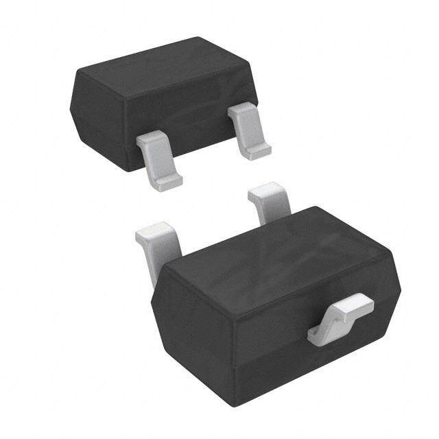
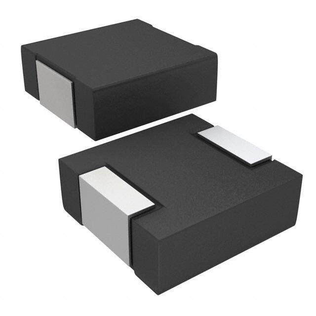
| 描述 | TRANS PREBIAS NPN 125MW SSMINI3 |
| 产品分类 | 晶体管(BJT) - 单路﹐预偏压式 |
| 品牌 | Panasonic Electronic Components |
| 数据手册 | http://industrial.panasonic.com/www-cgi/jvcr13pz.cgi?E+SC+4+BFA7001+UNR92A3G+8+WW |
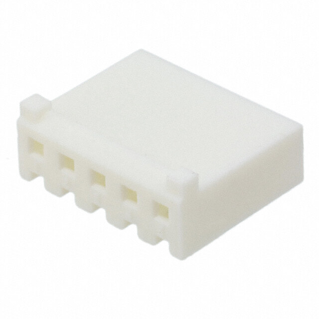
| 产品图片 |
|
| 产品型号 | UNR92A3G0L |
| rohs | 无铅 / 符合限制有害物质指令(RoHS)规范要求 |
| 产品系列 | - |
| 不同 Ib、Ic时的 Vce饱和值(最大值) | 250mV @ 300µA, 10mA |
| 不同 Ic、Vce 时的DC电流增益(hFE)(最小值) | 80 @ 5mA,10V |
| 产品目录绘图 |
|
| 产品目录页面 | |
| 供应商器件封装 | SS迷你型3-F3 |
| 其它名称 | UNR92A3G0LDKR |
| 功率-最大值 | 125mW |
| 包装 | Digi-Reel® |
| 安装类型 | 表面贴装 |
| 封装/外壳 | SC-89,SOT-490 |
| 晶体管类型 | NPN - 预偏压 |
| 标准包装 | 1 |
| 电压-集射极击穿(最大值) | 50V |
| 电流-集电极(Ic)(最大值) | 80mA |
| 电流-集电极截止(最大值) | 500nA |
| 电阻器-发射极基底(R2)(Ω) | 47k |
| 电阻器-基底(R1)(Ω) | 47k |
| 频率-跃迁 | 150MHz |


PDF Datasheet 数据手册内容提取
This product complies with the RoHS Directive (EU 2002/95/EC). Transistors with built-in Resistor UNR92A3G Silicon NPN epitaxial planar type For digital circuits Features / Package Optimum for high-density mounting and downsizing of the equipment e Code Contribute to low power consumption SSMini3-F3 c Pin Name 1:d Base Absolute Maximum Ratings T = 25°C n 2: Emitter a e 3: Collector Parameter Symbol Rating Unit e. a g Collector-base voltage (Emitter open) V 50 V a CBO u Marking Symboslt: FN Collector-emitter voltage (Base open) V 50 V e CEOn cl y Collector current IC 80 nmA Internal eCconnection TJSuotontarcalt igpoeon wt etememr pdpeiersarsatiupturaerteion nteTPTsTtjg –55n 11to22 t55+1i25 m°°CCW r Product lifB R R12 CE u o i o g f pe n. n y o CC ooElllleelecccttootrrr--ibecMmaaslie tC tveProh lvaatoaarrgalateamc g(teEeeD tm(reBirsiitattsiecers oo pp Teesnna ))=c 2e/5c°DiCs±cS3oVV°yCmnCtBibOnolueIIdC i ==pnl 12cal0 m numAedA,de , pI lsIE m amf= C=ana oii0 lo0lennntotdd eeiwtdindiinoiasansncsncwcocioenenn t ttitgi ynnpuUueemeRiddLc ttoayynb.ppopeeuadMt55 n00ilnaatseosnti Tic.yncpfoo.rjpm/aMetina/x UVVnit n CEO C B o e CCoolllleeccttoorr--bemasiet tceur tcouftfo cfuf rcruernarite n(ntEt me (Bnitataesre ooppeenn)) IICCBEOO VVCCBE == 5500 VV,, IIBEv i==s i00t follwww.s 00..15 mmAA Emitter-base cutoff currenMt (Collector open) IEBO VEB = 6e Vas, IeC = 0http:// 0.1 mA Forward current transfer ratio hFE VCE P=l 10 V, IC = 5 mA 80 Collector-emitter saturation voltage V I = 10 mA, I = 0.3 mA 0.25 V CE(sat) C B Output voltage high-level V V = 5 V, V = 0.5 V, R = 1 kW 4.9 V OH CC B L Output voltage low-level V V = 5 V, V = 3.5 V, R = 1 kW 0.2 V OL CC B L Input resistance R —30% 47 +30% kW 1 Resistance ratio R / R 0.8 1.0 1.2 1 2 Transition frequency f V = 10 V, I = —2 mA, f = 200 MHz 150 MHz T CB E Note) Measuring methods are based on JAPANESE INDUSTRIAL STANDARD JIS C 7030 measuring methods for transistors. Publication date: September 2007 SJH00245AED 1
This product complies with the RoHS Directive (EU 2002/95/EC). UNR92A3G UNR92A3G_PT-Ta UNR92A3G_IC-VCE UNR92A3G_VCE(sat)-IC P T I V V I T a C CE CE(sat) C 80 I = 1.0 mA V) 10 W) 120 Ta = 25°C B 0000....6789 mmmmAAAA (CE(sat) IC / IB = 10 m 0.5 mA V P (T mA) 60 00..34 mmAA age 1 Total power dissipation 4800 Collector current I (C 2400 ce/00..21 mmAA dctor-emitter saturation volt 10−1 Ta = 852°5C°C−25°C e 0 0 n Coll 10−2 0 40 80 120 0 4 8 e12 1 10 102 Ambient temperature Ta (°C) aCollector-emitter voltage VCE (V) Collectorg ceu.rrent IC (mA) a UNR92A3G_hFE-IC UNR92A3G_Cobu-VCB e UstNR92A3G_IO-VIN hFE IC n Cob VCB cl IO VIN y Forward current transfer ratio hFE1230000000M1 ColalUecNitRoTVr9D ac2 I=NuA 1 ri83r05eG°nnC _It2 OV 5−I°It2CNCsV5 - °IC(COmE =A 1)0ec VDi10s2cooCollector output capacitancenti (Common base, input open circuited) C (pF)nobue0241nd iCpnlotlcalleincuteodrde- pblsa mamfsneanao1i ilv0lenontotdlt eaewgdindiniena sas fTVg ncnc=a Cfc =oco1B oe 2neM n t 5tuti(tgi°HVr Cyn ynz1)pu0UpuP2reeeeRoddL dttoauyyOutput current I (mA)ncOb.ppt opeel111iua000df1t−−−01 n312el0acatseosntiIn icp.uncft ovo0.roj.8ltpma/gaeeti n /VoInN.VT (aO V=1 =. )62 55 °VC 102 VTO = c= 2 e05/.°2C V win mic an o e V (V)IN 10 Maintena se visit fp:o/l/lwww.s ge ea htt olta Pl v ut 1 p n I 10−1 10−1 1 10 102 Output current I (mA) O 2 SJH00245AED
This product complies with the RoHS Directive (EU 2002/95/EC). UNR92A3G SSMini3-F3 Unit: mm / +0.05 1.60−0.03 e +0.05 0.26−0.02 c 5 3 0.0d ± n 75 3 e0. e. a g +0.055−0.03 60 ±0.05 u e sta n 0.8 1. ycl n °) ec e (5 ct lif i u 1 2 d t t o r +0.05 (n0.50) (0.50) n r P 0.13−0.02 u 1.00 ±0.05 o i o g f pe n. n y o M a(5°) Disnce/cDiscontinued i0 to 0.10pnlcalnu+0.05e0.70d−0.03de pls mamfanaoiillenntotd eewdindiniasasoncncwcocioenenn t ttitgi ynnepuUueemeRiddLc ttoayynb.ppopeeuadt nlaatseosnti ic.ncfoo.rjpm/a(0.45)etin/ ntena sit follww.s ai vi w M se p:// ea htt Pl SJH00245AED 3
Request for your special attention and precautions in using the technical information and semiconductors described in this book (1)(cid:9)If any of the products or technical information described in this book is to be exported or provided to non-residents, the laws and regulations of the exporting country, especially, those with regard to security export control, must be observed. (2)(cid:9)The technical information described in this book is intended only to show the main characteristics and application circuit examples of the products, and no license is granted under any intellectual property right or other right owned by our company or any other company. Therefore, no responsibility is assumed by our company as to the infringement upon any such right owned by any other company which may arise as a result of the use of technical information described in this book. (3)(cid:9)The products described in this book are intended to be used for standard applications or general electronic equipment (such as office / equipment, communications equipment, measuring instruments and household appliances). Consult our sales staff in advance for information on the following applicateions: (cid:150) Special applications (such as for airplanes, aerospace, automobiles, traffic control equipment, combustion equipment, life support systems and safety devices) in which exceptional quality and reliability are required, or if the failure or malfunction of the prod- c ucts may directly jeopardize life or harm the human body. (cid:150) Any applications other than the standard applications intended. d n (4)(cid:9)The products and product specifications described in this book are subject to change without notice for modification and/or im- e provement. At the final stage of your design, purchasing, or use of the products, therefore, ask for the most upe-t.o-date Product Standards in advance to make sure that the latest spaecifications satisfy your requirements. ag u st (5)(cid:9)When designing your equipment, comply with the range of absolute maximum rating and the guarantee ed operating conditions (operating power supply voltage and opernating environment etc.). Especially, please be careful not to yexclceed the range of absolute maximum rating on the transient state, such as power-on, power-onff and mode-switching. Otherwiseec, we will not be liable for any (cid:9) dEevfeecnt wwhheicnh t hmea pyr aordiusec tlsa taerre i nu syeodeu wr eitqhuinip tmhee ngt.uaranteed values, take into the consideration ocf ti nlicfidence of break down and failure i u mode, possible to occur to semiconductor products. Measures on the systems such as redudndant design, arresting the spread of fire or preventing glitch are retcommended in order to prevetnt physical injury, fire, social damoages, for example, by using the products. r n n r P (6)(cid:9)Comply with the instructions for use in order to prevent breakdown and characteruistics change due to external factors (ESD, EOS, o tdhaemrmp-apl rostorfe spisa caknidn gm iesc rheaqnuiicraeld s, tsraetsiss)f ya tt hteho ec otinmdiet ioofn sh, asnudclhin ags, smheoluf nlitfine ga nodnr gtah tfe c eulsatpoysmepdeer t'sim per oscinecsse. fWirsht eonp eunsiinngg tphreo dpuaccktsa ogfoenrs. .which (7)(cid:9)TEMhleics trbioc oIkna dmusatyriD abl eCi noo.,t Lrtedps.rinted coDri srecproondtuicnedu ewdh ietpnhlecalr nuwedhdoe pllsly mamf aonaoiilrl ennptotda erewtdinidinaialsaslyncnc,c ocowenen ti tttitgih ynonupuUute eeRthddL e t topayynrb.pipoopere uadwt nrliatattseneo spntie ricm.ncfisoso.irjonpm/ oaetfi nM/atsushita ce/ win mic n o e ntena sit follww.s ai vi w M se p:// ea htt Pl